
Femtosecond Laser Fabrication of Curved Plasma Channels with Low Surface Roughness and High Circularity for Multistage Laser-Wakefield Accelerators

Abstract
:1. Introduction
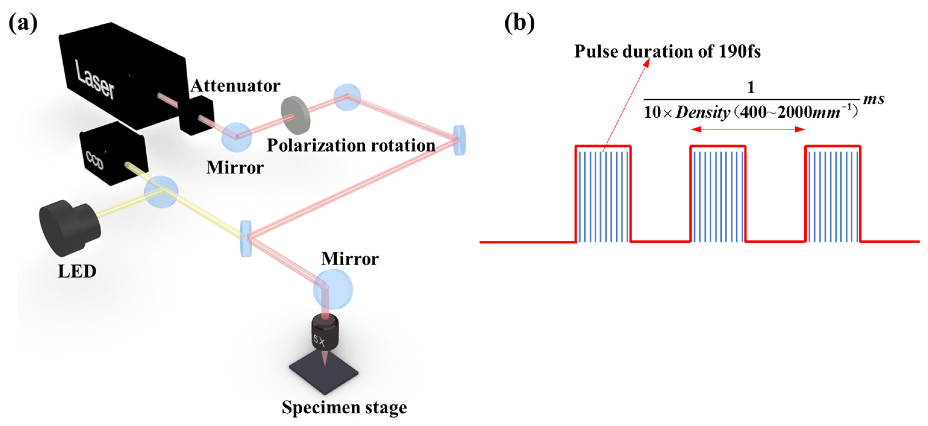
2. Experiments
3. Results and Discussion
3.1. Regression Model of Plasma Channel Mass
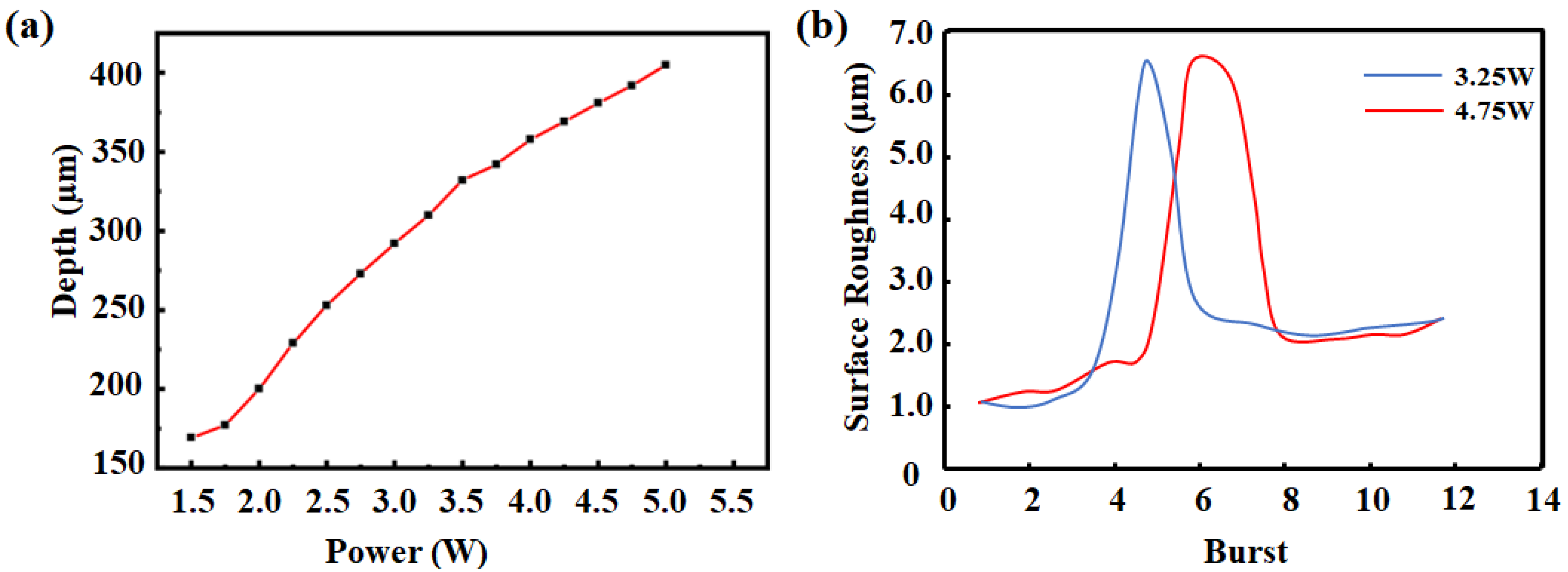
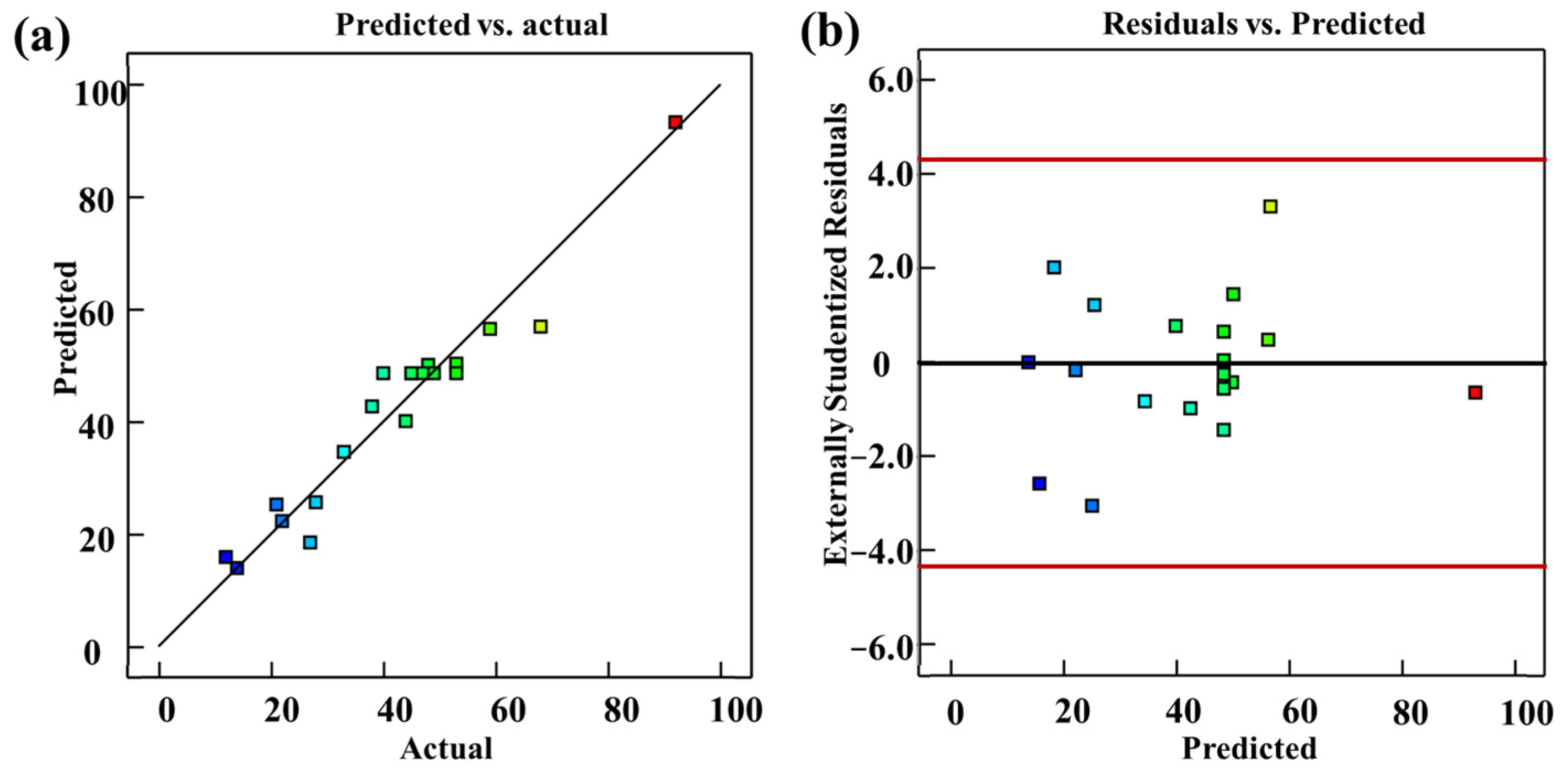
3.2. Feasibility of Fitted Model
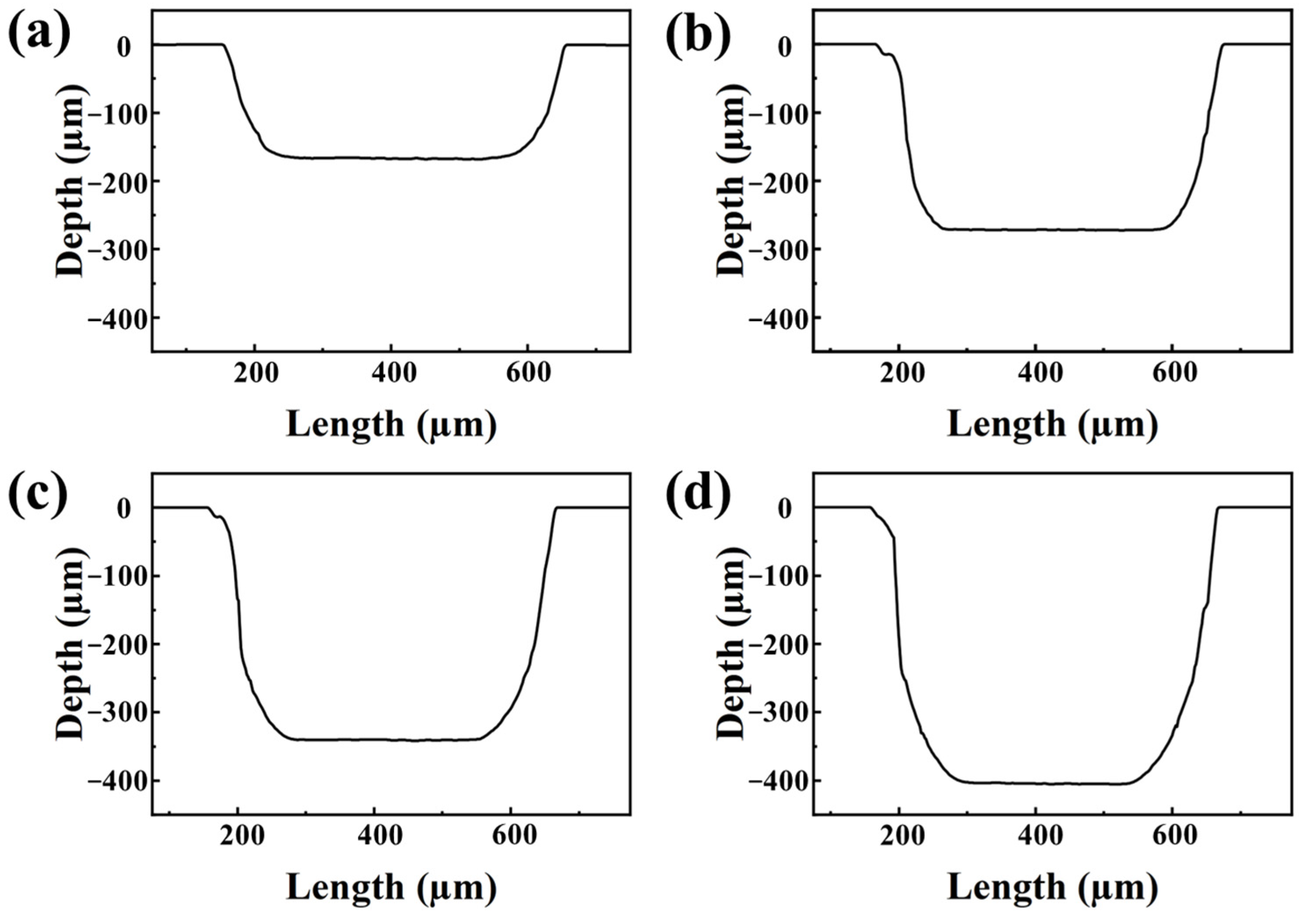
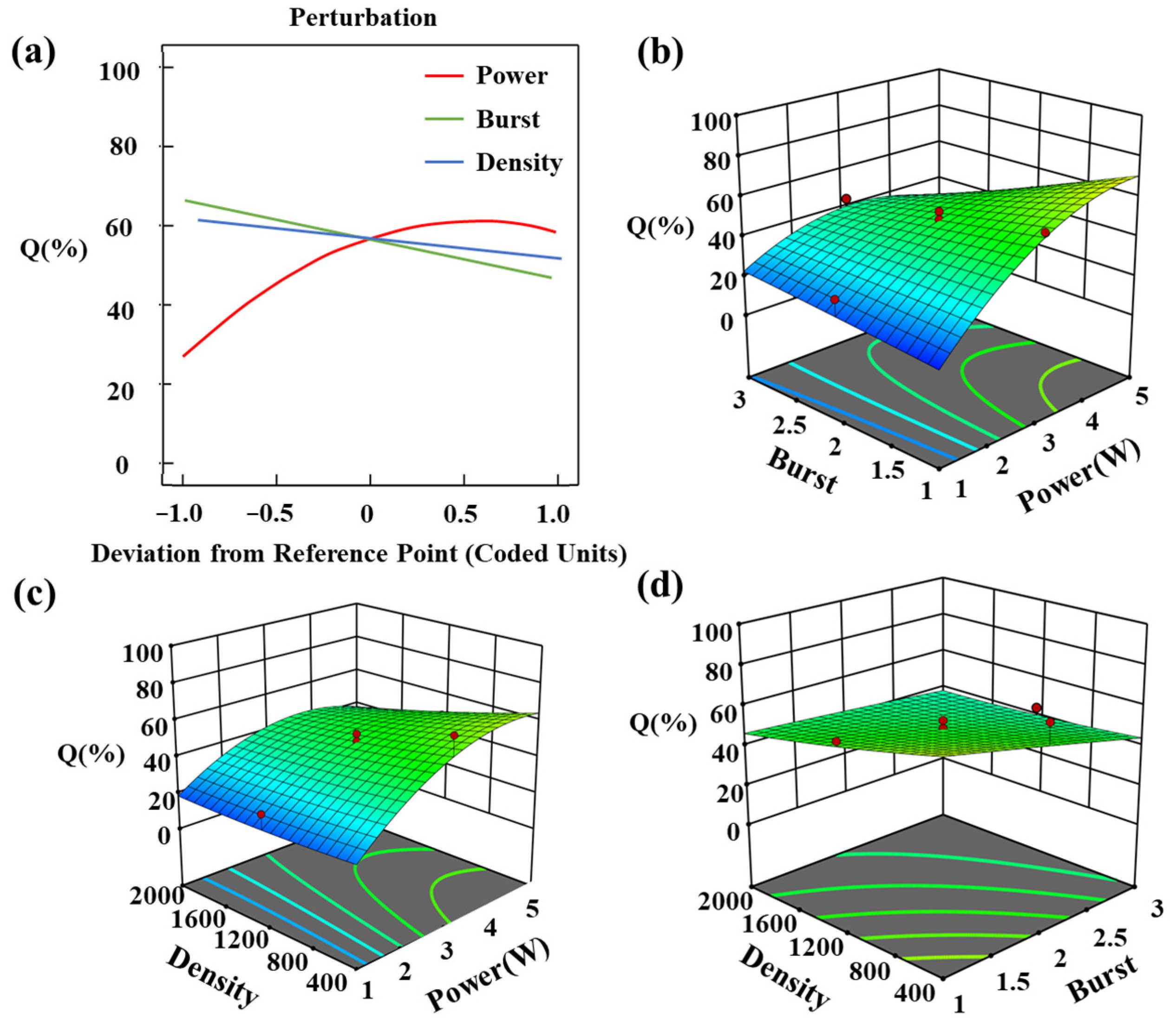
3.3. Parameter Optimization
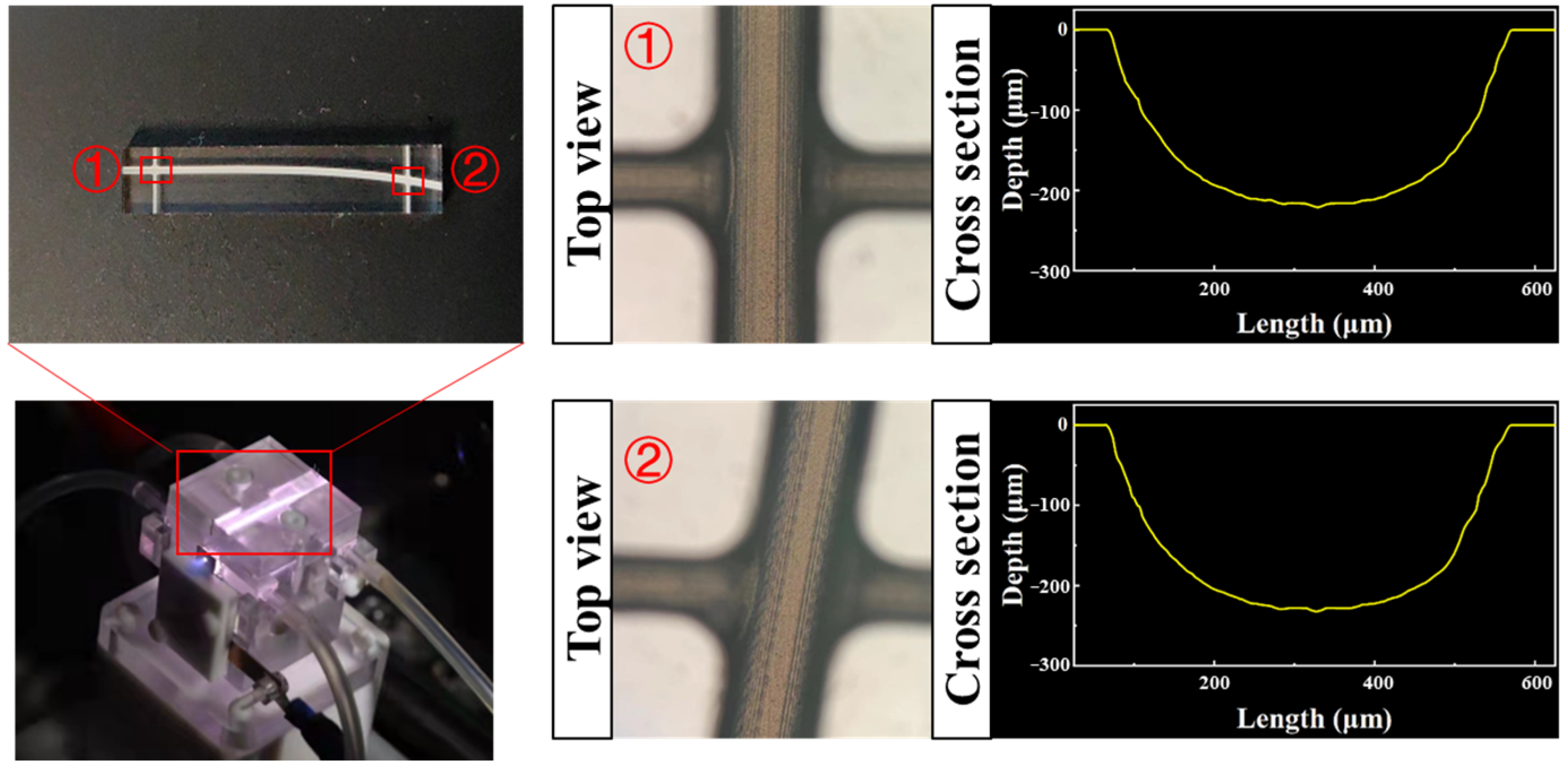
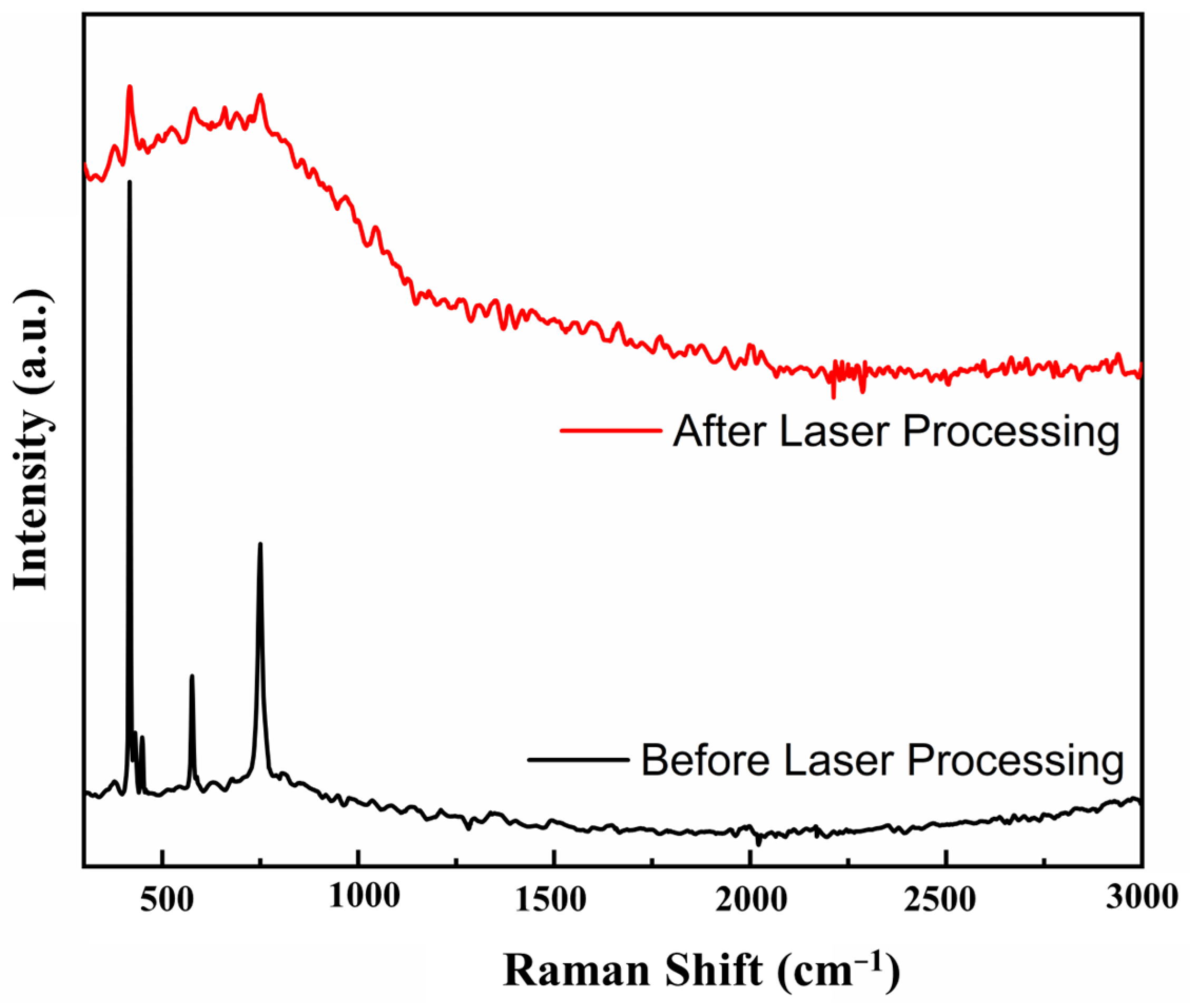
3.4. Product Inspection
4. Conclusions
Author Contributions
Funding
Institutional Review Board Statement
Informed Consent Statement
Data Availability Statement
Conflicts of Interest
References
- Shpakov, V.; Anania, M.P.; Behtouei, M.; Bellaveglia, M.; Biagioni, A.; Cesarini, M.; Chiadroni, E.; Cianchi, A.; Costa, G.; Croia, M.; et al. First emittance measurement of the beam-driven plasma wakefield accelerated electron beam. Phys. Rev. Accel. Beams 2021, 24, 051301. [Google Scholar] [CrossRef]
- Esarey, E.; Schroeder, C.B.; Leemans, W.P. Physics of laser-driven plasma-based electron accelerators. Rev. Mod. Phys. 2009, 81, 1229–1285. [Google Scholar] [CrossRef]
- Martins, S.F.; Fonseca, R.; Lu, W.; Mori, W.B.; Silva, L.O. Exploring laser-wakefield-accelerator regimes for near-term lasers using particle-in-cell simulation in Lorentz-boosted frames. Nat. Phys. 2010, 6, 311–316. [Google Scholar] [CrossRef]
- Kozlova, M.; Andriyash, I.; Gautier, J.; Sebban, S.; Smartsev, S.; Jourdain, N.; Chaulagain, U.; Azamoum, Y.; Tafzi, A.; Goddet, J.-P.; et al. Hard X Rays from Laser-Wakefield Accelerators in Density Tailored Plasmas. Phys. Rev. X 2020, 10, 011061. [Google Scholar] [CrossRef]
- Wang, W.; Feng, K.; Ke, L.; Yu, C.; Xu, Y.; Qi, R.; Chen, Y.; Qin, Z.; Zhang, Z.; Fang, M.; et al. Free-electron lasing at 27 nanometres based on a laser wakefield accelerator. Nature 2021, 595, 516–520. [Google Scholar] [CrossRef]
- Emma, C.; Xu, X.; Fisher, A.; Robles, R.; MacArthur, J.P.; Cryan, J.; Hogan, M.J.; Musumeci, P.; White, G.; Marinelli, A. Terawatt attosecond X-ray source driven by a plasma accelerator. APL Photonics 2021, 6, 076107. [Google Scholar] [CrossRef]
- Jiang, K.; Wang, W.; Feng, K.; Li, R. Review of Quality Optimization of Electron Beam Based on Laser Wakefield Acceleration. Photonics 2022, 9, 511. [Google Scholar] [CrossRef]
- Gonsalves, A.J.; Nakamura, K.; Daniels, J.; Benedetti, C.; Pieronek, C.; de Raadt, T.C.H.; Steinke, S.; Bin, J.H.; Bulanov, S.S.; van Tilborg, J.; et al. Petawatt Laser Guiding and Electron Beam Acceleration to 8 GeV in a Laser-Heated Capillary Discharge Waveguide. Phys. Rev. Lett. 2019, 122, 084801. [Google Scholar] [CrossRef]
- Steinke, S.; van Tilborg, J.; Benedetti, C.; Geddes, C.G.R.; Schroeder, C.B.; Daniels, J.; Swanson, K.K.; Gonsalves, A.J.; Nakamura, K.; Matlis, N.H.; et al. Multistage coupling of independent laser-plasma accelerators. Nature 2016, 530, 190–193. [Google Scholar] [CrossRef]
- Sokollik, T.; Shiraishi, S.; Osterhoff, J.; Evans, E.; Gonsalves, A.J.; Nakamura, K.; Van Tilborg, J.; Lin, C.; Toth, C.; Leemans, W.P.; et al. Tape-Drive Based Plasma Mirror. In AIP Conference Proceedings; American Institute of Physics: College Park, MD, USA, 2010; Volume 1299, p. 233. [Google Scholar] [CrossRef]
- Luo, J.; Chen, M.; Wu, W.Y.; Weng, S.M.; Sheng, Z.M.; Schroeder, C.B.; Jaroszynski, D.A.; Esarey, E.; Leemans, W.P.; Mori, W.B.; et al. Multistage Coupling of Laser-Wakefield Accelerators with Curved Plasma Channels. Phys. Rev. Lett. 2018, 120, 154801. [Google Scholar] [CrossRef]
- Qi, L.; Nishii, K.; Yasui, M.; Aoki, H.; Namba, Y. Femtosecond laser ablation of sapphire on different crystallographic facet planes by single and multiple laser pulses irradiation. Opt. Lasers Eng. 2010, 48, 1000–1007. [Google Scholar] [CrossRef]
- Wen, Q.; Zhang, P.; Cheng, G.; Jiang, F.; Lu, X. Crystalline orientation effects on material removal of sapphire by femtosecond laser irradiation. Ceram. Int. 2019, 45, 23501–23508. [Google Scholar] [CrossRef]
- Wang, K.; Jiang, F.; Yan, L.; Xu, X.; Wang, N.; Zha, X.; Lu, X.; Wen, Q. Study on mechanism of crack propagation of sapphire single crystals of four different orientations under impact load and static load. Ceram. Int. 2019, 45, 7359–7375. [Google Scholar] [CrossRef]
- Biagioni, A.; Anania, M.P.; Arjmand, S.; Behar, E.; Costa, G.; Del Dotto, A.; Ferrario, M.; Galletti, M.; Lollo, V.; Pellegrini, D.; et al. Gas-filled capillary-discharge stabilization for plasma-based accelerators by means of a laser pulse. Plasma Phys. Control. Fusion 2021, 636, 115013. [Google Scholar] [CrossRef]
- Vora, H.D.; Santhanakrishnan, S.; Harimkar, S.P.; Boetcher, S.K.S.; Dahotre, N.B. One-dimensional multipulse laser machining of structural alumina: Evolution of surface topography. Int. J. Adv. Manuf. Technol. 2013, 68, 69–83. [Google Scholar] [CrossRef]
- Chang, C.-W.; Chen, C.-Y.; Chang, T.-L.; Ting, C.-J.; Wang, C.-P.; Chou, C.-P. Sapphire surface patterning using femtosecond laser micromachining. Appl. Phys. A 2012, 109, 441–448. [Google Scholar] [CrossRef]
- Jaroszynski, D.; Bingham, R.; Brunetti, E.; Ersfeld, B.; Gallacher, J.; Van Der Geer, B.; Issac, R.; Jamison, S.; Jones, D.; De Loos, M.; et al. Radiation sources based on laser–plasma interactions. Philos. Trans. R. Soc. A Math. Phys. Eng. Sci. 2006, 364, 689–710. [Google Scholar] [CrossRef] [PubMed]
- Li, X.; Jia, T.; Feng, D.; Xu, Z. Ablation induced by femtosecond laser in sapphire. Appl. Surf. Sci. 2004, 225, 339–346. [Google Scholar] [CrossRef]
- Wei, H.; Huang, C.; Liu, H.; Liu, D.; Yao, P.; Chu, D. Modeling and optimizing femtosecond laser process parameters for high-efficient and near damage-free micromachining of single-crystal GaN substrate. Mater. Sci. Semicond. Process. 2023, 153, 107123. [Google Scholar] [CrossRef]
- Tan, J.-W.; Wang, G.; Zhao, G.-X.; Hou, Y.-C.; Sun, D.-R.; Song, Y.-F.; Dong, L.-Y.; Zhao, H.; Wang, Y. Femtosecond laser hybrid processing strategy of transparent hard and brittle materials. Front. Chem. 2022, 10. [Google Scholar] [CrossRef]
- Butkutė, A.; Sirutkaitis, R.; Gailevičius, D.; Paipulas, D.; Sirutkaitis, V. Sapphire Selective Laser Etching Dependence on Radiation Wavelength and Etchant. Micromachines 2022, 14, 7. [Google Scholar] [CrossRef]
- Wang, M.; Mei, W.; Wang, Y. Simulation of femtosecond laser ablation sapphire based on free electron density. Opt. Laser Technol. 2018, 113, 123–128. [Google Scholar] [CrossRef]
- Hribar, L.; Gregorčič, P.; Senegačnik, M.; Jezeršek, M. The Influence of the Processing Parameters on the Laser-Ablation of Stainless Steel and Brass during the Engraving by Nanosecond Fiber Laser. Nanomaterials 2022, 12, 232. [Google Scholar] [CrossRef] [PubMed]
- Pallares-Aldeiturriaga, D.; Claudel, P.; Granier, J.; Travers, J.; Guillermin, L.; Flaissier, M.-O.; D’augeres, P.B.; Sedao, X. Femtosecond Laser Engraving of Deep Patterns in Steel and Sapphire. Micromachines 2021, 12, 804. [Google Scholar] [CrossRef] [PubMed]
- Sundaram, S.K.; Mazur, E. Inducing and probing non-thermal transitions in semiconductors using femtosecond laser pulses. Nat. Mater. 2002, 1, 217–224. [Google Scholar] [CrossRef]
- Vilar, R.; Sharma, S.; Almeida, A.; Cangueiro, L.; Oliveira, V. Surface morphology and phase transformations of femtosecond laser-processed sapphire. Appl. Surf. Sci. 2014, 288, 313–323. [Google Scholar] [CrossRef]
- Juodkazis, S.; Nishimura, K.; Misawa, H.; Ebisui, T.; Waki, R.; Matsuo, S.; Okada, T. Control over the Crystalline State of Sapphire. Adv. Mater. 2006, 18, 1361–1364. [Google Scholar] [CrossRef]
- Juodkazis, S.; Kohara, S.; Ohishi, Y.; Hirao, N.; Vailionis, A.; Mizeikis, V.; Saito, A.; Rode, A. Structural Characterization of Femtosecond Laser Modified Regions Inside Sapphire. J. Nanosci. Nanotechnol. 2011, 11, 2931–2936. [Google Scholar] [CrossRef]
- Mizeikis, V.; Kimura, S.; Surovtsev, N.V.; Jarutis, V.; Saito, A.; Misawa, H.; Juodkazis, S. Formation of amorphous sapphire by a femtosecond laser pulse induced micro-explosion. Appl. Surf. Sci. 2009, 255, 9745–9749. [Google Scholar] [CrossRef]
- Wang, X.; Lim, G.; Zheng, H.; Ng, F.; Liu, W.; Chua, S. Femtosecond pulse laser ablation of sapphire in ambient air. Appl. Surf. Sci. 2004, 228, 221–226. [Google Scholar] [CrossRef]
- Capuano, L.; Tiggelaar, R.; Berenschot, J.; Gardeniers, J.; Römer, G. Fabrication of millimeter-long structures in sapphire using femtosecond infrared laser pulses and selective etching. Opt. Lasers Eng. 2020, 133, 106114. [Google Scholar] [CrossRef]
- Esarey, E.; Schroeder, C.B.; Shadwick, B.A.; Wurtele, J.S.; Leemans, W.P. Nonlinear Theorey of Nonparaxial Laser Pulse Propagation in Plasmas Channels. Phys. Rev. Lett. 2000, 84, 3081. [Google Scholar] [CrossRef] [PubMed]
- Li, J.; Li, B.; Zhu, X.; Bi, Z.; Wen, X.; Lu, L.; Yuan, X.; Liu, F.; Chen, M. Generation of curved plasma channel from a discharged capillary for intense laser guiding. High Power Laser Sci. Eng. 2023, submitted.
- Zhu, X.; Li, B.; Liu, F.; Li, J.; Bi, Z.; Ge, X.; Deng, H.; Zhang, Z.; Cui, P.; Lu, L.; et al. Experimental demonstration of laser guiding and wakefield acceleration in a curved plasma channel. Phys. Rev. Lett. 2023, in press.


| Source | df | F-Value | p-Value | Remarks |
|---|---|---|---|---|
| Model | 9 | 12.32 | 0.0003 | Significant |
| A-P | 1 | 43.84 | <0.0001 | |
| B-B | 1 | 11.81 | 0.0064 | |
| C-D | 1 | 8.85 | 0.0139 | |
| AB | 1 | 22.39 | 0.0008 | |
| AC | 1 | 4.85 | 0.0523 | |
| BC | 1 | 2.39 | 0.1531 | |
| A2 | 1 | 9.90 | 0.0104 | |
| B2 | 1 | 0.0049 | 0.9456 | |
| C2 | 1 | 0.0675 | 0.8004 | |
| Lack of Fit | 5 | 4.96 | 0.0517 | Not significant |
Disclaimer/Publisher’s Note: The statements, opinions and data contained in all publications are solely those of the individual author(s) and contributor(s) and not of MDPI and/or the editor(s). MDPI and/or the editor(s) disclaim responsibility for any injury to people or property resulting from any ideas, methods, instructions or products referred to in the content. |
© 2023 by the authors. Licensee MDPI, Basel, Switzerland. This article is an open access article distributed under the terms and conditions of the Creative Commons Attribution (CC BY) license (https://creativecommons.org/licenses/by/4.0/).
Share and Cite
Deng, H.; Zhang, Z.; Chen, M.; Li, J.; Cao, Q.; Hu, X. Femtosecond Laser Fabrication of Curved Plasma Channels with Low Surface Roughness and High Circularity for Multistage Laser-Wakefield Accelerators. Materials 2023, 16, 3278. https://doi.org/10.3390/ma16083278
Deng H, Zhang Z, Chen M, Li J, Cao Q, Hu X. Femtosecond Laser Fabrication of Curved Plasma Channels with Low Surface Roughness and High Circularity for Multistage Laser-Wakefield Accelerators. Materials. 2023; 16(8):3278. https://doi.org/10.3390/ma16083278
Chicago/Turabian StyleDeng, Hongyang, Ziyang Zhang, Min Chen, Jianlong Li, Qiang Cao, and Xuejiao Hu. 2023. "Femtosecond Laser Fabrication of Curved Plasma Channels with Low Surface Roughness and High Circularity for Multistage Laser-Wakefield Accelerators" Materials 16, no. 8: 3278. https://doi.org/10.3390/ma16083278