Article

Towards Room Temperature Phase Transition of W-Doped VO2 Thin Films Deposited by Pulsed Laser Deposition: Thermochromic, Surface, and Structural Analysis

1
Université de Lyon, Université Jean Monnet-Saint-Étienne, CNRS, Institut d’Optique Graduate School, Laboratoire Hubert Curien, UMR 5516, F-42023 Saint-Etienne, France
2
Mines Saint-Etienne, Université de Lyon, CNRS, UMR 5307 LGF, Centre SMS, F-42023 Saint-Etienne, France
*
Author to whom correspondence should be addressed.
Materials 2023, 16(1), 461; https://doi.org/10.3390/ma16010461
Submission received: 5 December 2022 / Revised: 21 December 2022 / Accepted: 30 December 2022 / Published: 3 January 2023

Abstract

:
Vanadium dioxide (VO2) with an insulator-to-metal (IMT) transition (∼68 °C) is considered a very attractive thermochromic material for smart window applications. Indeed, tailoring and understanding the thermochromic and surface properties at lower temperatures can enable room-temperature applications. The effect of W doping on the thermochromic, surface, and nanostructure properties of VO2 thin film was investigated in the present proof. W-doped VO2 thin films with different W contents were deposited by pulsed laser deposition (PLD) using V/W (+O2) and V2O5/W multilayers. Rapid thermal annealing at 400–450 °C under oxygen flow was performed to crystallize the as-deposited films. The thermochromic, surface chemistry, structural, and morphological properties of the thin films obtained were investigated. The results showed that the V5+ was more surface sensitive and W distribution was homogeneous in all samples. Moreover, the V2O5 acted as a W diffusion barrier during the annealing stage, whereas the V+O2 environment favored W surface diffusion. The phase transition temperature gradually decreased with increasing W content with a high efficiency of −26 °C per at. % W. For the highest doping concentration of 1.7 at. %, VO2 showed room-temperature transition (26 °C) with high luminous transmittance (62%), indicating great potential for optical applications.

Graphical Abstract

1. Introduction

VO2 has the closest phase transition to room temperature of any the thermochromic oxide materials and has consequently been extensively studied for a variety of applications including electronic switches, smart windows, memory devices, RF microwave switches, and terahertz metamaterial devices [1,2,3,4,5]. Indeed, VO2 enables insulator-to-metal transition (IMT) as well as transition from a monoclinic (M1) to a rutile structure (R) at around 68 °C [6]. However, the phase transition temperature of pristine VO2 thin films is too high for room temperature applications. To meet the demand for a broad range of room temperature applications, considerable efforts have been made to reduce the phase transition temperature. One way to do so is replacing V4+ ions by metal ions with higher valences such as W6+, Nb5+, and Mo6+ [7,8,9,10], among which W has been considered one of the most effective dopants. Interestingly, the doping of W into the VO2 matrix affects the transition characteristics. The substitutional doping of the W6+ to replace V4+ has been shown to lead to a remarkable reduction in the phase transition temperature, i.e., 20–28 °C per W at. % [7,10,11,12,13,14]. VO2-based thin films can be synthesized using several techniques including sol-gel [15], magnetron sputtering [16,17], chemical vapor deposition [18], and pulsed laser deposition (PLD). However, there have been few reports on synthesizing W-doped VO2 films using PLD [19,20,21,22], which is known to be a versatile method to control doping in thin films. Komal et al. [23] used mixed V2O3 and WO3 pellets as targets for the PLD process and observed that the VO2 doped with 1.5 at. % of W reduced the phase transition temperature towards room temperature (27 °C). Émond et al. [24] used PLD to prepare W-doped VO2 films with a phase transition temperature of 36 °C. Soltani et al. [25] manufactured 1.6 at. % W-doped VO2 thin films using a W-doped vanadium oxide target. The phase transition temperature was about 36 °C and all-optical switching was demonstrated at a telecommunication wavelength of 1.55 µm. S. S. Majid et al. [26] used a W-doped target and obtained W-doped VO2 films with a significantly lower phase transition temperature (∼19 °C for 1.3% W) by stabilizing the metallic rutile phase R. All these studies demonstrate that PLD is a versatile method capable of tuning the properties of VO2. However, they used either a target mixture of tungsten and vanadium oxide or a co-ablation process and mainly focused on reducing the phase transition temperature. In the present work, an innovative method to synthesize W-doped VO2 thin films using pulsed laser deposition is proposed. This method consists in fabricating multilayers composed of V/W (+O2) and V2O5/W bilayers, followed by rapid thermal annealing to allow both crystallization of VO2 and the diffusion of W through the VO2 layers to synthetize homogeneous W-doped VO2 thin films. The main advantage of this process over co-ablation deposition is its repeatability. Indeed, co-ablation can cause problems of thickness and of non-homogeneous composition as well as contamination between the targets. In addition to the synthesis process, this work not only aims to reduce the phase transition temperature but also to improve our understanding of the surface chemistry of W-doped films. For the latter, angle-resolved X-ray photoelectron spectroscopy (ARXPS), which is rarely used in VO2-reported studies, was used to measure the concentration of vanadium, the depth of tungsten oxidation, as well as to assess their depth distribution.

2. Materials and Methods

2.1. Synthesis of W-Doped VO2 Thin Films Using Pulsed Laser Deposition

W-doped VO2 thin films were synthesized by rapid thermal annealing of multilayers composed of VOX/W bilayers as illustrated in the figure inserted in Table 1. The bilayers were deposited on fused silica substrates using pulsed laser deposition (PLD) at room temperature. The PLD chamber was evacuated to a background pressure of 2 × 10⁻⁷ mbar. Three types of targets were used in the investigation: Vanadium (V), Vanadium pentoxide (V2O5), and Tungsten (W), all at 99.9% purity. A KrF excimer laser (wavelength 248 nm, repetition rate 10 Hz, fluence 13 J/cm2) was used to ablate the targets. The target/substrate distance was 5 cm. The laser beam was oriented with an angle of 45° to the target. For the W-doped VOX using metallic vanadium as a precursor, the oxygen pressure inside the deposition chamber was 1 × 10⁻² mbar when ultrapure O2 was used. For the W-doped VOX using the V2O5 target, ablation was performed without oxygen gas. During the deposition process, the targets were rotated to enable uniform ablation. For all depositions, the deposition rate obtained by profilometry was around 6.3 nm/min for V+O2, 6.4 nm/min for V2O5, and 1.37 nm/min for W. The alternative ablation sequences of V2O5 (or V in O2) and W were adjusted to obtain three multilayers (A, B, C) with different W contents to obtain three W-doped VOX thin films with a similar total thickness of 20 nm (Table 1).
The rapid thermal annealing process was performed using an RTP furnace (AS-One RTP system from Annealsys, Montpellier, France). For samples A and B, the annealing temperature was 400 °C for 120 s, while for sample C, the annealing temperature was 450 °C for 60 s. The time of rapid thermal annealing was adjusted from preliminary experiments, depending on the two different precursors, to ensure the observation of the thermochromic transition in both cases. All the annealing processes were carried out at an oxygen partial pressure of 1 mbar and a 50 sccm flow. The heating rate was 5 °C/s and the cooling was natural. The annealing chamber was evacuated to a 1 × 10⁻² mbar before the oxygen was introduced. Undoped VO2 thin films were obtained using a similar process for the purpose of comparison.

2.2. Characterization of the Undoped VO2 and W-Doped VO2 Films

The composition and dopant profile were investigated using XPS analysis using a Thermo VG Theta probe spectrometer (Thermo Fisher Scientific, Invitrogen, Waltham, MA, USA) with a focused monochromatic AlKα source (hν = 1486.68 eV, 400 μm spot size) and photoelectrons were collected using a concentric hemispherical analyzer. A constant ΔE mode and a 2D channel plate detector (Thermo Fisher Scientific, Invitrogen, Waltham, MA, USA) were used. The energy scale was calibrated with sputter-cleaned pure reference samples of Au, Ag, and Cu such that Au4f7/2, Ag3d5/2, and Cu3p3/2 were positioned at binding energies of 83.98, 386.26, and 932.67 eV, respectively. Angle-resolved XPS analyses were performed thanks to the ability of the spectrometer to simultaneously collect several photoelectron emission angles in the acceptance range of 60° without tilting the sample. Charge neutralization was applied during analysis. High-resolution spectra (i.e., O1s-V2p, V3p-W4f) were fitted using AVANTAGE software version 5.9 by Thermo Fisher Scientific. The structure of the films was analyzed by Raman analysis (Jobin-Yvon ARAMIS) using a Helium-Neon laser source (Horiba Jobin Yvon, Gières, France) at an excitation wavelength of 633 nm, a laser power of 0.1 mW, focused with a 100× objective, consistent with a spot diameter of less than 1 mm. Atomic force microscopy (AFM) (Icon BRUKER, Berlin, Germany) and scanning electron microscopy (SEM) (JEOL IT 800 SHL, Tokyo, Japan) were used to analyze the topography, roughness, and morphology of the films. The thermochromic properties of the films were measured by collecting the transmittance in a temperature range between 15 and 100 °C using a fiber optic spectrometer (Ocean Insight, Duiven, The Netherlands) equipped with handmade heating units in the visible (400–800 nm) and IR (900–2500 nm) wavelength ranges. For the undoped and W-doped VO2 thin films, the integrated luminous transmittance (Tlum, 380–780 nm) and solar modulation efficiency (Tsol, 300–2500 nm) were deduced from the following equation:
Tlum, sol = (∫φlum, sol (λ)T(λ)dλ)/(∫φlum, sol (λ)dλ)
where T(λ) is film transmittance at wavelength (λ), φlum(λ) is the standard luminous efficiency depending on the photopic vision of human eye, φsol(λ) is the solar irradiance spectrum (air mass 1.5) corresponding to the sun at an angle of 37° to the horizon [23]. ΔTsol is obtained from ΔTsol = Tsol (15 °C) − Tsol (100 °C) and Tlum = (Tlum (15 °C) + Tlum (100 °C)/2).

3. Results and Discussion

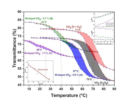
3.1. Thermochromic Properties

To investigate the influence of W-doping on thermochromic properties, the transmittance of the samples during a heating and cooling phase were recorded and plotted the hysteresis loops of undoped and W-doped thin films.
Figure 1a shows the hysteresis loop produced by plotting the temperature dependence of transmittance of undoped and W-doped VO2 thin films at a fixed wavelength of 1500 nm. The switching temperatures during heating (Tt,h) and cooling (Tt,c) were determined from the half-value width of each curve and the average temperature of commutation (Tt) representative of thermochromic behavior was defined as Tt = (Tt,h + Tt,c)/2. Both undoped VO2 films had a phase transition temperature Tt of 70–71 °C (quite similar whatever the precursors).
The dependence of the phase transition temperature on the tungsten content was linear (Figure 1b). W doping significantly reduced Tt to ~−26 °C per at. % W, as shown in Figure 1b, which is in line with reported values of ~20–28 °C per at. % W [7,12,13,14]. The Tt reduction mechanism of the W-doped VO2 can be ascribed to free electron carriers generation [27] as well as to the extra strain resulting from the atom replacement of V4+ by W6+. This induced high symmetry around the W atom, implying transformation into a rutile structure [28,29], which was subsequently corroborated by Raman analysis.
Hysteresis behavior is another important thermochromic parameter of VO2-based thin films. The hysteresis loop width gradually narrowed from 11 °C for the VO2 film to 4 °C for the film doped with 1.7 at. % W, as can be seen in Figure 2a. This illustrates that the W dopant not only reduces the transition temperature but also reduces the width of the hysteresis loop. Previous studies suggested that ΔT is closely linked to the grain size, lattice stress, impurity phase, and crystallinity of VO2 film [30,31]. Structural defects induced by W doping act as nucleation sites of the phase transition [32,33]. Therefore, the activation energy of the phase transition would be reduced, with a decrease in hysteresis width. The result is promising, as narrow hysteresis loops are required to create devices with rapid commutations.
Moreover, the luminous transmittance (Tlum) and the solar modulation ability (ΔTsol) are plotted in Figure 2b. Compared to undoped VO2 thin films, the luminous transmittance of the W-doped VO2 thin films was higher. Indeed, Tlum increased with increasing W content. The luminous transmittance of the W-rich sample was 62.2%, a rather very good performance for W-doped VO2 thin films. In the literature, the luminous transmittance of VO2 after W-doping usually either remained unchanged or decreased, as reported in Table 2. In the present study, our W-doped VO2 thin films had higher Tlum. Further investigations would be necessary to identify the exact origin of such a significant increase of Tlum at the two highest W contents. The solar modulation ability ΔTsol decreased gradually with increasing W content. This is consistent with the results of previous works [34,35], in which ΔTsol decreased with increasing W content. The variation of ΔTsol depending on W content is in good agreement with the variation of Tt. Two explanations are possible: the incorporation of W induces a destabilization of VO2 (M) lattice, and reduces the phase transition temperature. On the other hand, too much W doping leads to an excess of free electrons, thereby deteriorating the phase transition property [36]. Overall, as shown in Table 2, our W-doped VO2 thin films outperformed other reported works on W-doped VO2 using different synthesis methods in terms of reducing Tt and improving luminous transmittance.

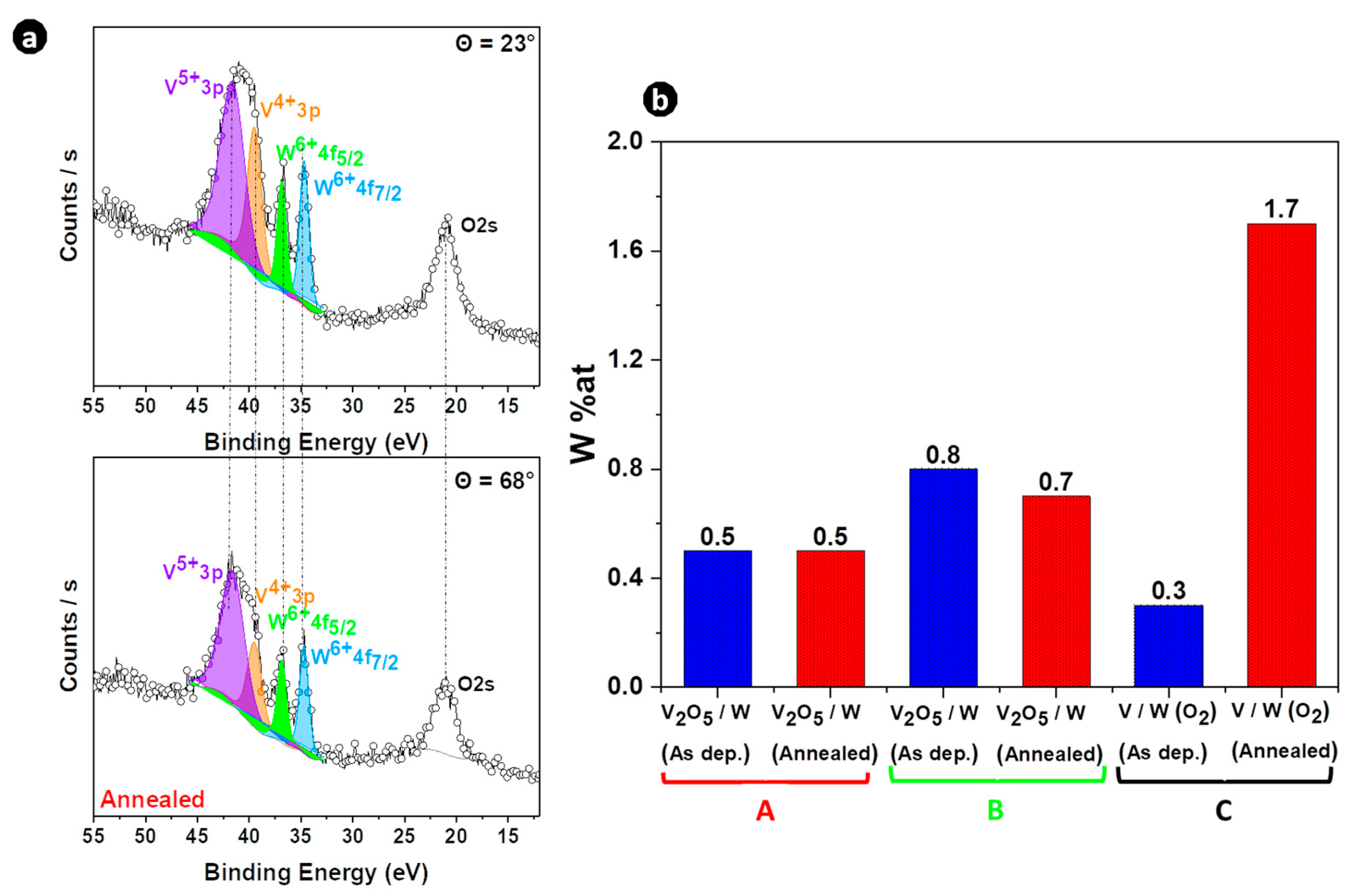
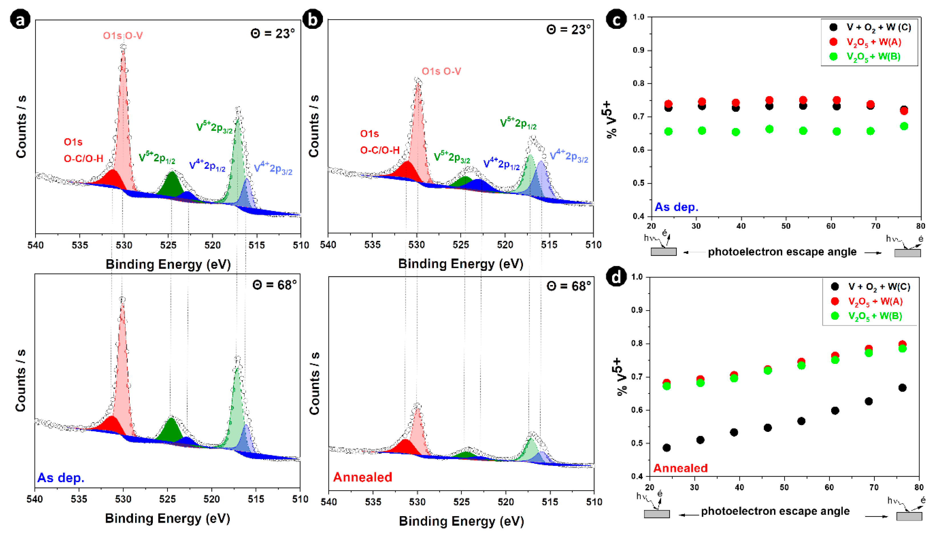
3.2. Surface Chemistry Analysis: Composition and Depth Distribution

To analyze the surface chemistry, the high-resolution XPS spectra of V 2p and W 4d core-levels of W-doped VOX (as-deposited) and W-doped VO2 (after annealing) thin films are shown in Figure 3a,b, respectively.
The W peaks of W 4d5/2 and W 4d3/2 were located at 246.8 and 259.8 eV, respectively, reflecting the + 6 oxidation state of W ions in both thin films [11,12,41,44]. The V 2p core-level was split into two regions, V 2p3/2 located at 516.9 eV and V 2p1/2 located around 524 eV [45,46], with the O1s located at 530 eV. The intensity of vanadium and oxygen peaks is not the same for all films, especially when the two deposition precursors V/W (O2) and V2O5/W are compared. Since the intensity of the tungsten peak differed from one sample to another, the W content differed. The presence of W can also be confirmed by its W 4f valence state [11]. The angle-resolved XPS spectra of W 4f core-levels at 23 and 68° of sample C are shown in Figure 2a after thermal annealing. Two strong peaks of W 4f core-level located at 34.7 eV and 36.9 eV were assigned to W 4f7/2 and W 4f5/2, respectively. This revealed that W6+ cations were present in W-doped VO2 thin films in line with previous reported work [47], and confirmed the successful W-doping of VO2 thin films. Furthermore, the atomic concentrations of W were calculated based on the XPS spectra of V 3p and W 4f and the results of the quantification are shown in Figure 4b.
Figure 4b reports W content in each sample before and after annealing. The annealing process did not significantly affect W content when the V2O5 target was used for W-doped VO2 synthesis (samples A and B) because almost identical W contents were found consecutive to the annealing treatment. This suggests that V2O5 may act as a barrier to the surface diffusion of W. On the contrary, using the vanadium target, an increase in the W content after thermal annealing (sample C) was observed. This means that W diffused more towards the VO2 surface during annealing and suggests that the V+O2 environment favors the surface diffusion of W. Such an increase in W content during annealing was also recently reported by Ström et al. [48]. In their study, the W content in steel increased during thermal annealing and the modified composition was attributed to a near-surface effect. This might also be the case in our study, with surface diffusion of W towards the VO2 surface during the annealing process.
For more insight into the depth distribution of W, Figure 5a,b show the dependence of the W6+ proportion as a function of the detection angle (23 to 76°) for all the samples before and after thermal annealing.
Similar W distribution between as-deposited and annealed films in samples A and B showed that the inter-diffusion between VOX and W layers occurred at room temperature during deposition. In other words, the inter-diffusion process and the crystallization process occurred separately. Diffusion occurred during PLD deposition while crystallization occurred during the thermal annealing stage. Conversely, with sample C, the different W distribution between as-deposited and annealed films showed that the inter-diffusion between VOX and W layers was not completed during PLD deposition, but was completed during the thermal annealing stage. This surface diffusion leads to an increase in W content toward the surface after thermal annealing. Therefore, along the first nanometers probed by ARXPS, sample C was richer in W after thermal annealing, while samples A and B had lower W contents. In addition, W distribution was almost constant with few discrepancies irrespective of the sample (before and after annealing), meaning that the W distribution was homogeneous in all the samples.
It is generally accepted that in addition to the doping element, the valence states of V can significantly affect the thermochromic characteristics of VO2-based thin films. Figure 6a,b show the high-resolution spectra of V 2p—O 1s recorded in XPS angle-resolved mode at two photoelectron take-off angles (23° and 68°) before and after thermal annealing for the W-rich sample (C). Deconvolution analysis of the V 2p3/2 and V 2p1/2 regions revealed two vanadium components in the samples, corresponding to V4+ and V5+ valence states: V4+ located at 516.1 eV for 2p3/2, and 522.8 eV for 2p1/2 with V5+ centered at 517.1 eV for 2p3/2, and 524.5 eV for 2p1/2 [45,46]. The binding energies of the peaks at 515.8 eV and 517.2 eV are close to those reported for VO2 (515.7–516.2 eV) and V2O5 (516.9–517.2 eV), respectively [45,49,50]. There was no significant shift in the position of the peak in terms of the binding energy of the as-deposited and annealed samples. However, no difference in the intensity of the two oxidation states V4+ and V5+ was observed: the intensity of the V4+ oxidation state increased while that of V5+ decreased after thermal annealing. The O 1s peak is deconvoluted into two peaks, one corresponding to the O-C/O-H bond, which appeared at 531.2 eV due to surface contamination of the films. The other peak was due to the O-V bond located at 529.9 eV [51].
To investigate the depth distribution of the V5+ oxidation state of vanadium, the spectra of V 2p were measured at various detection angles ranging from 23° to 76° using angle-resolved X-ray photoelectron spectroscopy. Figure 6c,d shows the dependence of the concentration of the V5+ oxidation state as a function of the detection angle for all the samples before and after thermal annealing. It can be seen from Figure 6c that the angle dependence of V5+ oxidation state concentration is quite similar to that before thermal annealing, indicating homogeneous distribution of V5+ on the surface of all samples. After thermal annealing (Figure 5d), the proportion of the V5+ oxidation state increased with the increase in the detection angle in all samples. The results of angle-resolved measurements confirmed that the outer part of the W-doped VO2 thin films was enriched in V5+, especially when the V2O5 target was used for the synthesis of W-doped VO2 films and hence, that the other V4+ oxidation state is located in the inner region of the films. To summarize, sample C was poorer in V5+ and richer in W while samples A and B were richer in V5+ and poorer in W after thermal annealing.

3.3. Structural and Morphological Analysis

The structural change that occurred with W doping at room temperature was investigated using Raman analysis.
Figure 7 shows the Raman spectra of the undoped and W-doped thin films at room temperature. The two undoped VO2 films (black and red curves in Figure 7) had typical peaks at 143 (Ag), 192 (Ag), 222 (Ag), 262 (Bg), 306 (Ag), 338 (Ag), 389 (Ag), 441 (Bg), 498 (Ag), and 617 (Ag) cm−1, corresponding to the monoclinic VO2 (M1) phase [52,53,54]. No vibration peak of V2O5 was observed, perhaps due to the low concentration of V2O5 resulting in weaker molecular vibration. Concerning the W-doped VO2 films, a decrease in the intensities of the Raman active modes (low-frequency and high-frequency mode) and broadening of the peaks with an increase on the percentage of W doping were observed. This can be explained by the fact that W doping starts to favor a more symmetric rutile structure. A similar effect has already been reported for W-doped VO2 films [23,55] and Nb-doped VO2 films [56]. Moreover, the 617 (Ag) cm−1 phonon mode was slightly upshifted and broadened as well as being reduced in intensity with W doping up to 625 cm−1 (green curve), indicating a distorted M1 phase and the nucleation of rutile domains at this stage [57]. In the W-rich sample (1.7 at. % W), some modes started to disappear (purple curve), indicating the beginning of the metallic rutile phase as observed in the above-mentioned analysis of the phase transition temperature.
Changes in the surface morphology and variations in the surface roughness of the undoped and W-doped VO2 thin films were investigated by SEM and AFM, respectively. Regarding the thin films obtained using V+O2 deposition, the surface morphology of undoped film (Figure 8a) was flat with trace-like cracks whereas with W doping, the surface of the film contained holes resembling pores. The surface morphology of the films deposited from the V2O5 target was uniform, dense, and compact, the undoped film being slightly smoother than the W-doped film. The difference in morphology between undoped and W-doped VO2 films can be attributed to the general regularity observed in solid solution formation: an increase in the number of constituents can play a role in the crystallization of the films [58,59]. AFM scanning maps of the films obtained from V+O2 exhibited a slight decrease in the root mean square (RMS) from the undoped to W-doped VO2 films. The RMS of the W-doped VO2 film obtained from V2O5, was slightly higher than that of the undoped film. However, the low RMS values indicate that our VO2-based thin films are extraordinarily smooth with improved quality compared to those obtained using other synthesis methods [60,61].

4. Conclusions

An innovative PLD method was developed to synthesize smooth W-doped thin films using V/W (+O2) and V2O5/W multilayers with subsequent post-rapid thermal annealing. Our results revealed that the inter-diffusion between the W and VOX layers was completed during the PLD deposition process at room temperature when the V2O5 target was used, whereas when the V+O2 source was used, inter-diffusion between the W and VOX layers was completed during the thermal annealing stage. Therefore, the V2O5 acted as a W diffusion barrier, while the V+O2 environment favored surface diffusion of W during the annealing stage. These findings also show that the V5+ is more surface sensitive and that the distribution of W on the surface of the samples is homogeneous. Furthermore, as expected, W doping leads to a sharp decrease in the VO2 IMT by a highly efficient reduction of the phase transition temperature −26 °C per at. % W. With W-doping of 1.7 at. %, the concentration of V5+ decreased, and the transition temperature of VO2 dropped to room temperature (26 °C), accompanied by a high luminous transmittance (62%) while retaining a narrow hysteresis width. These very good thermochromic properties have high potential in the application of smart windows and optical devices based on thermochromic switching behavior.

Author Contributions

Conceptualization, C.D. and F.G.; Methodology, F.B. and A.-S.L.; Investigation, Y.B. and V.B.; Writing–Original Draft Preparation, Y.B.; Writing–Review & Editing, Y.B. and C.D.; Visualization, C.D.; Supervision, C.D., F.B. and F.G.; Project Administration, F.B. and C.D. All authors have read and agreed to the published version of the manuscript.

Funding

This research was funded by the LABEX MANUTECH-SISE (ANR-10-LABX-0075) of Université de Lyon.

Data Availability Statement

Data is available from the corresponding author upon reasonable request.

Acknowledgments

This work was supported by the LABEX MANUTECH-SISE (ANR-10-LABX-0075) of Université de Lyon, in the framework of Plan France 2030 operated by the French National Research Agency (ANR).

Conflicts of Interest

The authors declare no conflict of interest.

References

  1. Chen, S.; Wang, Z.; Ren, H.; Chen, Y.; Yan, W.; Wang, C.; Li, B.; Jiang, J.; Zou, C. Gate-Controlled VO2 Phase Transition for High-Performance Smart Windows. Sci. Adv. 2019, 5, eaav6815. [Google Scholar] [CrossRef] [PubMed] [Green Version]
  2. Mizsei, J.; Lappalainen, J.; Pohl, L. Active Thermal-Electronic Devices Based on Heat-Sensitive Metal-Insulator-Transition Resistor Elements. Sens. Actuators A Phys. 2017, 267, 14–20. [Google Scholar] [CrossRef]
  3. Beaumont, A.; Leroy, J.; Orlianges, J.-C.; Crunteanu, A. Current-Induced Electrical Self-Oscillations across out-of-Plane Threshold Switches Based on VO2 Layers Integrated in Crossbars Geometry. J. Appl. Phys. 2014, 115, 154502. [Google Scholar] [CrossRef]
  4. Vardi, N.; Anouchi, E.; Yamin, T.; Middey, S.; Kareev, M.; Chakhalian, J.; Dubi, Y.; Sharoni, A. Ramp-Reversal Memory and Phase-Boundary Scarring in Transition Metal Oxides. Adv. Mater. 2017, 29, 1605029. [Google Scholar] [CrossRef] [PubMed] [Green Version]
  5. Lee, J.; Lee, D.; Cho, S.J.; Seo, J.-H.; Liu, D.; Eom, C.-B.; Ma, Z. Epitaxial VO2 Thin Film-Based Radio-Frequency Switches with Thermal Activation. Appl. Phys. Lett. 2017, 111, 063110. [Google Scholar] [CrossRef]
  6. Ji, Y.D.; Pan, T.S.; Bi, Z.; Liang, W.Z.; Zhang, Y.; Zeng, H.Z.; Wen, Q.Y.; Zhang, H.W.; Chen, C.L.; Jia, Q.X.; et al. Epitaxial Growth and Metal-Insulator Transition of Vanadium Oxide Thin Films with Controllable Phases. Appl. Phys. Lett. 2012, 101, 071902. [Google Scholar] [CrossRef]
  7. Burkhardt, W.; Christmann, T.; Meyer, B.K.; Niessner, W.; Schalch, D.; Scharmann, A. W- and F-Doped VO2 Films Studied by Photoelectron Spectrometry. Thin Solid Film. 1999, 345, 229–235. [Google Scholar] [CrossRef]
  8. Guan, S.; Souquet-Basiège, M.; Toulemonde, O.; Denux, D.; Penin, N.; Gaudon, M.; Rougier, A. Toward Room-Temperature Thermochromism of VO2 by Nb Doping: Magnetic Investigations. Chem. Mater. 2019, 31, 9819–9830. [Google Scholar] [CrossRef]
  9. Khan, G.R.; Asokan, K.; Ahmad, B. Room Temperature Tunability of Mo-Doped VO2 Nanofilms across Semiconductor to Metal Phase Transition. Thin Solid Film. 2017, 625, 155–162. [Google Scholar] [CrossRef]
  10. Piccirillo, C.; Binions, R.; Parkin, I.P. Nb-Doped VO2 Thin Films Prepared by Aerosol-Assisted Chemical Vapour Deposition. Eur. J. Inorg. Chem. 2007, 2007, 4050–4055. [Google Scholar] [CrossRef]
  11. Chen, S.-E.; Lu, H.-H.; Brahma, S.; Huang, J.-L. Effects of Annealing on Thermochromic Properties of W-Doped Vanadium Dioxide Thin Films Deposited by Electron Beam Evaporation. Thin Solid Film. 2017, 644, 52–56. [Google Scholar] [CrossRef]
  12. Romanyuk, A.; Steiner, R.; Marot, L.; Oelhafen, P. Temperature-Induced Metal–Semiconductor Transition in W-Doped VO2 Films Studied by Photoelectron Spectroscopy. Sol. Energy Mater. Sol. Cells 2007, 91, 1831–1835. [Google Scholar] [CrossRef]
  13. Tang, C.; Georgopoulos, P.; Fine, M.E.; Cohen, J.B.; Nygren, M.; Knapp, G.S.; Aldred, A. Local Atomic and Electronic Arrangements in WxV1−xO2. Phys. Rev. B 1985, 31, 1000–1011. [Google Scholar] [CrossRef] [PubMed]
  14. Jin, P.; Tazawa, M.; Ikeyama, M.; Tanemura, S.; Macák, K.; Wang, X.; Olafsson, S.; Helmersson, U. Growth and Characterization of Epitaxial Films of Tungsten-Doped Vanadium Oxides on Sapphire (110) by Reactive Magnetron Sputtering. J. Vac. Sci. Technol. A 1999, 17, 1817–1821. [Google Scholar] [CrossRef]
  15. Lee, Y.W.; Kim, B.-J.; Lim, J.-W.; Yun, S.J.; Choi, S.; Chae, B.-G.; Kim, G.; Kim, H.-T. Metal-Insulator Transition-Induced Electrical Oscillation in Vanadium Dioxide Thin Film. Appl. Phys. Lett. 2008, 92, 162903. [Google Scholar] [CrossRef]
  16. Karaoglan-Bebek, G.; Hoque, M.N.F.; Holtz, M.; Fan, Z.; Bernussi, A.A. Continuous Tuning of W-Doped VO2 Optical Properties for Terahertz Analog Applications. Appl. Phys. Lett. 2014, 105, 201902. [Google Scholar] [CrossRef] [Green Version]
  17. Yu, S.; Wang, S.; Lu, M.; Zuo, L. A Metal-Insulator Transition Study of VO2 Thin Films Grown on Sapphire Substrates. J. Appl. Phys. 2017, 122, 235102. [Google Scholar] [CrossRef]
  18. Sahana, M.B.; Subbanna, G.N.; Shivashankar, S.A. Phase Transformation and Semiconductor-Metal Transition in Thin Films of VO2 Deposited by Low-Pressure Metalorganic Chemical Vapor Deposition. J. Appl. Phys. 2002, 92, 6495–6504. [Google Scholar] [CrossRef]
  19. Ahmed, N.; Mahmood, R.; Umar, Z.A.; Liaqat, U.; ul Haq, M.A.; Ahmed, R.; Ahmad, P.; Raza, S.R.A.; Baig, M.A. Near Room Temperature, SMT and Visible Photo-Response in Pulsed Laser Deposited VO2 (M1) Thin Films. Phys. B Condens. Matter 2022, 635, 413841. [Google Scholar] [CrossRef]
  20. Umar, Z.A.; Ahmed, N.; Ahmed, R.; Arshad, M.; Anwar-Ul-Haq, M.; Hussain, T.; Baig, M.A. Substrate Temperature Effects on the Structural, Compositional, and Electrical Properties of VO2 Thin Films Deposited by Pulsed Laser Deposition. Surf. Interface Anal. 2018, 50, 297–303. [Google Scholar] [CrossRef]
  21. Bhardwaj, D.; Goswami, A.; Umarji, A.M. Synthesis of Phase Pure Vanadium Dioxide (VO2) Thin Film by Reactive Pulsed Laser Deposition. J. Appl. Phys. 2018, 124, 135301. [Google Scholar] [CrossRef]
  22. Bleu, Y.; Bourquard, F.; Jamon, D.; Loir, A.-S.; Garrelie, F.; Donnet, C. Tailoring Thermochromic and Optical Properties of VO2 Thin Films by Pulsed Laser Deposition Using Different Starting Routes. Opt. Mater. 2022, 133, 113004. [Google Scholar] [CrossRef]
  23. Mulchandani, K.; Soni, A.; Pathy, K.; Mavani, K.R. Structural Transformation and Tuning of Electronic Transitions by W-Doping in VO2 Thin Films. Superlattices Microstruct. 2021, 154, 106883. [Google Scholar] [CrossRef]
  24. Émond, N.; Ibrahim, A.; Torriss, B.; Hendaoui, A.; Al-Naib, I.; Ozaki, T.; Chaker, M. Impact of Tungsten Doping on the Dynamics of the Photo-Induced Insulator-Metal Phase Transition in VO2 Thin Film Investigated by Optical Pump-Terahertz Probe Spectroscopy. Appl. Phys. Lett. 2017, 111, 092105. [Google Scholar] [CrossRef]
  25. Soltani, M.; Chaker, M.; Haddad, E.; Kruzelecky, R.V.; Nikanpour, D. Optical Switching of Vanadium Dioxide Thin Films Deposited by Reactive Pulsed Laser Deposition. J. Vac. Sci. Technol. A 2004, 22, 859–864. [Google Scholar] [CrossRef]
  26. Majid, S.S.; Sahu, S.R.; Ahad, A.; Dey, K.; Gautam, K.; Rahman, F.; Behera, P.; Deshpande, U.; Sathe, V.G.; Shukla, D.K. Role of V-V Dimerization in the Insulator-Metal Transition and Optical Transmittance of Pure and Doped VO2 Thin Films. Phys. Rev. B 2020, 101, 014108. [Google Scholar] [CrossRef] [Green Version]
  27. Goodenough, J.B. The Two Components of the Crystallographic Transition in VO2. J. Solid State Chem. 1971, 3, 490–500. [Google Scholar] [CrossRef]
  28. Asayesh-Ardakani, H.; Nie, A.; Marley, P.M.; Zhu, Y.; Phillips, P.J.; Singh, S.; Mashayek, F.; Sambandamurthy, G.; Low, K.; Klie, R.F.; et al. Atomic Origins of Monoclinic-Tetragonal (Rutile) Phase Transition in Doped VO2 Nanowires. Nano Lett. 2015, 15, 7179–7188. [Google Scholar] [CrossRef]
  29. Tan, X.; Yao, T.; Long, R.; Sun, Z.; Feng, Y.; Cheng, H.; Yuan, X.; Zhang, W.; Liu, Q.; Wu, C.; et al. Unraveling Metal-Insulator Transition Mechanism of VO2Triggered by Tungsten Doping. Sci. Rep. 2012, 2, 466. [Google Scholar] [CrossRef] [Green Version]
  30. Zheng, T.; Sang, J.; Hua, Z.; Xu, L.; Xu, X.; Wang, C.; Wu, B. A Simple Method for Synthesizing VO2 with Almost Coincident Hysteresis Loops on Si Substrate Containing TiO2 Buffer Layer. J. Alloys Compd. 2021, 865, 158755. [Google Scholar] [CrossRef]
  31. Suh, J.Y.; Lopez, R.; Feldman, L.C.; Haglund, R.F. Semiconductor to Metal Phase Transition in the Nucleation and Growth of VO2 Nanoparticles and Thin Films. J. Appl. Phys. 2004, 96, 1209–1213. [Google Scholar] [CrossRef]
  32. Jin, P.; Nakao, S.; Tanemura, S. Tungsten Doping into Vanadium Dioxide Thermochromic Films by High-Energy Ion Implantation and Thermal Annealing. Thin Solid Film. 1998, 324, 151–158. [Google Scholar] [CrossRef]
  33. Lopez, R.; Haynes, T.E.; Boatner, L.A.; Feldman, L.C.; Haglund, R.F. Size Effects in the Structural Phase Transition of VO2 Nanoparticles. Phys. Rev. B 2002, 65, 224113. [Google Scholar] [CrossRef]
  34. Hu, L.; Tao, H.; Chen, G.; Pan, R.; Wan, M.; Xiong, D.; Zhao, X. Porous W-Doped VO2 Films with Simultaneously Enhanced Visible Transparency and Thermochromic Properties. J. Sol-Gel Sci. Technol. 2016, 77, 85–93. [Google Scholar] [CrossRef]
  35. Li, B.; Tian, S.; Tao, H.; Zhao, X. Tungsten Doped M-Phase VO2 Mesoporous Nanocrystals with Enhanced Comprehensive Thermochromic Properties for Smart Windows. Ceram. Int. 2019, 45, 4342–4350. [Google Scholar] [CrossRef]
  36. Shen, N.; Chen, S.; Shi, R.; Niu, S.; Amini, A.; Cheng, C. Phase Transition Hysteresis of Tungsten Doped VO2 Synergistically Boosts the Function of Smart Windows in Ambient Conditions. ACS Appl. Electron. Mater. 2021, 3, 3648–3656. [Google Scholar] [CrossRef]
  37. Zomaya, D.; Xu, W.Z.; Grohe, B.; Mittler, S.; Charpentier, P.A. W-Doped VO2/PVP Coatings with Enhanced Thermochromic Performance. Sol. Energy Mater. Sol. Cells 2019, 200, 109900. [Google Scholar] [CrossRef]
  38. Zou, J.; Chen, X.; Xiao, L. Phase Transition Performance Recovery of W-Doped VO2 by Annealing Treatment. Mater. Res. Express 2018, 5, 065055. [Google Scholar] [CrossRef]
  39. Dang, Y.; Zhao, L.; Liu, J. Preparation and Optical Properties of W-Doped VO2/AZO Bilayer Composite Film. Ceram. Int. 2020, 46, 9079–9085. [Google Scholar] [CrossRef]
  40. Zhang, L.; Xia, F.; Yao, J.; Zhu, T.; Xia, H.; Yang, G.; Liu, B.; Gao, Y. Facile Synthesis, Formation Mechanism and Thermochromic Properties of W-Doped VO2 (M) Nanoparticles for Smart Window Applications. J. Mater. Chem. C 2020, 8, 13396–13404. [Google Scholar] [CrossRef]
  41. Shen, N.; Chen, S.; Chen, Z.; Liu, X.; Cao, C.; Dong, B.; Luo, H.; Liu, J.; Gao, Y. The Synthesis and Performance of Zr-Doped and W–Zr-Codoped VO2 Nanoparticles and Derived Flexible Foils. J. Mater. Chem. A 2014, 2, 15087–15093. [Google Scholar] [CrossRef]
  42. Liang, Z.; Zhao, L.; Meng, W.; Zhong, C.; Wei, S.; Dong, B.; Xu, Z.; Wan, L.; Wang, S. Tungsten-Doped Vanadium Dioxide Thin Films as Smart Windows with Self-Cleaning and Energy-Saving Functions. J. Alloys Compd. 2017, 694, 124–131. [Google Scholar] [CrossRef]
  43. Wang, S.; Wei, W.; Huang, T.; Yuan, M.; Yang, Y.; Yang, W.; Zhang, R.; Zhang, T.; Chen, Z.; Chen, X.; et al. Al-Doping-Induced VO2 (B) Phase in VO2 (M) Toward Smart Optical Thin Films with Modulated ΔTvis and ΔTc. Adv. Eng. Mater. 2019, 21, 1900947. [Google Scholar] [CrossRef]
  44. Takami, H.; Kanki, T.; Ueda, S.; Kobayashi, K.; Tanaka, H. Electronic Structure of W-Doped VO2 Thin Films with Giant Metal–Insulator Transition Investigated by Hard X-Ray Core-Level Photoemission Spectroscopy. Appl. Phys. Express 2010, 3, 063201. [Google Scholar] [CrossRef]
  45. Sawatzky, G.A.; Post, D. X-Ray Photoelectron and Auger Spectroscopy Study of Some Vanadium Oxides. Phys. Rev. B 1979, 20, 1546–1555. [Google Scholar] [CrossRef]
  46. Zhang, Z.; Gao, Y.; Chen, Z.; Du, J.; Cao, C.; Kang, L.; Luo, H. Thermochromic VO2 Thin Films: Solution-Based Processing, Improved Optical Properties, and Lowered Phase Transformation Temperature. Langmuir 2010, 26, 10738–10744. [Google Scholar] [CrossRef]
  47. Li, D.; Zhao, Z.; Wang, C.; Deng, S.; Yang, J.; Wang, X.; Li, J.; Zhao, Y.; Jin, H. Influence of the Charge Compensation Effect on the Metal–Insulator Transition of Mg-W Co-Doped VO2. Appl. Surf. Sci. 2022, 579, 151990. [Google Scholar] [CrossRef]
  48. Ström, P.; Primetzhofer, D. In-Situ Measurement of Diffusion and Surface Segregation of W and Ta in Bare and W-Coated EUROFER97 during Thermal Annealing. Nucl. Mater. Energy 2021, 27, 100979. [Google Scholar] [CrossRef]
  49. Demeter, M.; Neumann, M.; Reichelt, W. Mixed-Valence Vanadium Oxides Studied by XPS. Surf. Sci. 2000, 454–456, 41–44. [Google Scholar] [CrossRef]
  50. Silversmit, G.; Depla, D.; Poelman, H.; Marin, G.B.; De Gryse, R. Determination of the V2p XPS Binding Energies for Different Vanadium Oxidation States (V5+ to V0+). J. Electron Spectrosc. Relat. Phenom. 2004, 135, 167–175. [Google Scholar] [CrossRef]
  51. Lee, D.; Kim, H.; Kim, J.W.; Lee, I.J.; Kim, Y.; Yun, H.-J.; Lee, J.; Park, S. Hydrogen Incorporation Induced the Octahedral Symmetry Variation in VO2 Films. Appl. Surf. Sci. 2017, 396, 36–40. [Google Scholar] [CrossRef]
  52. Shvets, P.; Dikaya, O.; Maksimova, K.; Goikhman, A. A Review of Raman Spectroscopy of Vanadium Oxides. J. Raman Spectrosc. 2019, 50, 1226–1244. [Google Scholar] [CrossRef]
  53. Schilbe, P. Raman Scattering in VO2. Phys. B Condens. Matter 2002, 316–317, 600–602. [Google Scholar] [CrossRef]
  54. Srivastava, R.; Chase, L.L. Raman Spectrum of Semiconducting and Metallic VO2. Phys. Rev. Lett. 1971, 27, 727–730. [Google Scholar] [CrossRef]
  55. Gu, D.; Zhou, X.; Sun, Z.; Jiang, Y. Influence of Gadolinium-Doping on the Microstructures and Phase Transition Characteristics of VO2 Thin Films. J. Alloys Compd. 2017, 705, 64–69. [Google Scholar] [CrossRef]
  56. Ji, C.; Wu, Z.; Wu, X.; Feng, H.; Wang, J.; Huang, Z.; Zhou, H.; Yao, W.; Gou, J.; Jiang, Y. Optimization of Metal-to-Insulator Phase Transition Properties in Polycrystalline VO2 Films for Terahertz Modulation Applications by Doping. J. Mater. Chem. C 2018, 6, 1722–1730. [Google Scholar] [CrossRef]
  57. Whittaker, L.; Wu, T.-L.; Stabile, A.; Sambandamurthy, G.; Banerjee, S. Single-Nanowire Raman Microprobe Studies of Doping-, Temperature-, and Voltage-Induced Metal–Insulator Transitions of WxV1−XO2 Nanowires. ACS Nano 2011, 5, 8861–8867. [Google Scholar] [CrossRef] [PubMed]
  58. Liu, X.; Wang, S.-W.; Chen, F.; Yu, L.; Chen, X. Tuning Phase Transition Temperature of VO2 Thin Films by Annealing Atmosphere. J. Phys. D Appl. Phys. 2015, 48, 265104. [Google Scholar] [CrossRef]
  59. Zhao, Z.; Li, J.; Ling, C.; Zhao, X.; Zhao, Y.; Jin, H. Electric Field Driven Abnormal Increase in Conductivity of Tungsten-Doped VO2 Nanofilms. Thin Solid Film. 2021, 725, 138643. [Google Scholar] [CrossRef]
  60. Ivanov, A.V.; Tatarenko, A.Y.; Gorodetsky, A.A.; Makarevich, O.N.; Navarro-Cía, M.; Makarevich, A.M.; Kaul, A.R.; Eliseev, A.A.; Boytsova, O.V. Fabrication of Epitaxial W-Doped VO2 Nanostructured Films for Terahertz Modulation Using the Solvothermal Process. ACS Appl. Nano Mater. 2021, 4, 10592–10600. [Google Scholar] [CrossRef]
  61. Pan, G.; Yin, J.; Ji, K.; Li, X.; Cheng, X.; Jin, H.; Liu, J. Synthesis and Thermochromic Property Studies on W Doped VO2 Films Fabricated by Sol-Gel Method. Sci. Rep. 2017, 7, 6132. [Google Scholar] [CrossRef] [PubMed]
Figure 1. (a) Hysteresis loops derived from the temperature-dependent transmittance of the undoped and W-doped (A, B, and C) thin films at a wavelength of 1500 nm. (b) The correlation between the phase transition temperature Tt and W concentration.
Materials 16 00461 g001
Figure 2. (a) Phase transition temperature (red) and hysteresis width (blue) for undoped and W-doped VO2 thin films. (b) The corresponding luminous transmittance (Tlum, orange) and the solar modulation ability (ΔTsol, in green) values.
Materials 16 00461 g002
Figure 3. V 2p and W 4d core-level XPS spectra of (a) W-doped VOX as-deposited thin films, and (b) W-doped VO2 thin films after rapid thermal annealing.
Materials 16 00461 g003
Figure 4. (a) Fitted ARXPS spectra of V 3p, W 4f, and O 2s core-levels for sample C after thermal annealing, at detection angles of 23° and 68°. (b) Quantification of W based on O 2s, W 4f, and V 3p peaks of the different samples before and after rapid thermal annealing.
Materials 16 00461 g004
Figure 5. The proportion of W6+ based on V 3p, W 4f, and O 2s as a function of the ARXPS detection angle for all the samples (a) before thermal annealing and (b) after thermal annealing.
Materials 16 00461 g005
Figure 6. Fitted ARXPS spectra of V 2p and O 1s core-levels for sample C at detection angles of 23° and 68°, respectively, (a) before thermal annealing and (b) after thermal annealing. The concentration of the V5+ oxidation state of vanadium was obtained from the fitted spectra of the V 2p electrons as a function of the angle of detection in all the samples, (c) before thermal annealing and (d) after thermal annealing.
Materials 16 00461 g006
Figure 7. Raman spectra of undoped and W-doped VO2 (samples A, B, and C) thin films.
Materials 16 00461 g007
Figure 8. Top-view SEM micrographs of the obtained thin films after rapid thermal annealing (a) VO2 thin film obtained from V+O2. (b) W-doped VO2 (1.7 at. % W, sample C). (c) VO2 thin film obtained from V2O5. (d) W-doped VO2 thin film (0.7 at. % W, sample B). The inserts correspond to the AFM images.
Materials 16 00461 g008
Table 1. Condition of deposited multilayers using pulsed laser deposition. The ablated thickness per layer and the number of individual layers were adjusted to obtain three different W contents (next investigated using XPS).
Materials 16 00461 i001Sample ASample BSample C
V ablated thickness per layer (nm)//0.283
V2O5 ablated thickness per layer (nm)0.2830.270/
W ablated thickness per layer (nm)0.0150.030.015
Number of VOx and W layers676767
Total thickness (nm)202020
Table 2. Comparison of some of the W-doped VO2 reported works on thermochromic parameters including Tt, ΔT, Tlum, and ΔTsol, with those of our present study. The terms « unchanged, increased, decreased » correspond to changes in the Tlum and ΔTsol values of W-doped VO2 compared to those of undoped VO2.
W (at. %)Tt (°C)∆T (°C)Tlum∆TsolProcessStructural FormRef.
0.14646.8UnchangedDecreasedElectron beam evaporationThin film[11]
22815UnchangedDecreasedSpin coatingThin film[37]
0.443/IncreasedDecreasedHydrothermalMesoporous film[38]
0.83620.5DecreasedDecreasedHydrothermalNanoparticles[39]
344.418.4IncreasedIncreasedSpin coatingCoating[40]
243/DecreasedDecreasedMicroemulsion technologyNanostructure[41]
1.355/DecreasedDecreasedMagnetron sputteringThin film[42]
1.317.525.1IncreasedDecreasedHydrothermalNanoparticle[43]
0.7416IncreasedDecreasedPLDThin filmThis work
1.7264IncreasedDecreasedPLDThin filmThis work
Disclaimer/Publisher’s Note: The statements, opinions and data contained in all publications are solely those of the individual author(s) and contributor(s) and not of MDPI and/or the editor(s). MDPI and/or the editor(s) disclaim responsibility for any injury to people or property resulting from any ideas, methods, instructions or products referred to in the content.

