1. Introduction
Nowadays, the applications of gallium nitride (GaN) and related compounds-based devices are very broad and high impurity doping via extrinsic sources is the key for its fabrication. For a long time silicon (Si) was the most common n-type GaN dopant and the growth of Si-doped GaN is largely controlled over a wide range of carrier densities from low-10
17 to mid-10
19 cm
−3. However, in view of some structural problems occurring in heavily doped films, germanium (Ge) became, over time, the second competitor of n-type doping. While doping GaN to low and intermediate concentrations using Si and Ge has become routine, compensation mechanisms are activated under very high donor doping, limiting the maximum electron concentration achievable with either dopant. The metal-insulator transition in GaN occurs at the critical concentration of uncompensated donors equal to approximately 1.6 × 10
18 cm
−3 [
1]. So, n-type GaN material, with free carrier concentrations higher than this critical value can be considered as a disordered system because of the high concentration of dopant atoms randomly distributed in the lattice.
To properly describe the transport phenomena in a disordered system, some quantum corrections are necessary. Within the framework of the semi classical Drude–Boltzmann model for the electrical conductivity, the quantum mechanical scattering of carriers at individual impurities is considered, but the coherent motion between scattering events and multiple scattering are neglected. However, the developing of scattering theories in which phase-coherent multiple scattering was systematically taken into account, showed that it yields a quantum correction to the conductance [
2]. Electrons in a disordered sample may be scattered in either direction and the quantum correction arises when the electron travels along a closed diffusive trajectory. This phenomenon called “weak localization” enhances the resistance above the classical Drude value [
3]. If one considers the case of wave functions that are scattered by the same centers (defects or impurities) but propagate in opposite directions along the same closed trajectory and, therefore, return to the origin with equal phases (systems with time reversal symmetry), then due to the coherence of both wave functions the quantum mechanical return probability is enhanced by a factor of two compared to the classical contribution to the return probability. In this sense one can talk about enhanced backscattering, carrier weak localization, as a result of quantum interference. As this additional scattering intensity exists only in the backscattering direction, it leads to an increase in the resistance of the material and lasts as long as the coherence of the scattered wave is not destroyed. The destruction of this interference is usually related to processes of electron inelastic scattering which are taken into account by electron–electron and electron–phonon interactions. The spin effect as spin-orbit coupling or spin-flip scattering by magnetic impurities also destroys the phase coherence.
However, a special role in breaking the wave function coherency is related to the magnetic field [
4]. In the presence of vector potential caused by the magnetic field, the two waves propagating in the opposite directions acquire a phase difference 2eΦ/c, where Φ is the magnetic flux through the area enclosed by the electron trajectory. This phase difference breaks the constructive interference and restores the conductivity to the value it would have without the quantum interference corrections. This is observed as an increase in conductivity with magnetic field, the effect called as negative magnetoresistivity (nMR). Thus, in principle, the low-temperature electron–electron and electron–phonon interactions can be extracted from weak-localization measurements under magnetic field, which therefore represent a powerful tool for studying relaxation mechanisms of conduction electrons which is the focus of this paper.
In the case of semiconductors, while at the beginning of the development of theoretical models of localization, the research concerned low temperature effects (below 10 K) in three-dimensional (3D) systems [
5,
6,
7,
8,
9,
10,
11,
12], over time, most experimental measurements reported in the literature were focused on low-dimensional structures such as semiconductor inversion layers, heterostructures with two-dimensional electron gas, or one-dimensional semiconductor wires and their corresponding, specific theoretical models. It resulted from the interest in new structures but also from the fact that the 3D case required a large disorder to obtain localization and still quantum-interference effects are comparatively small and much less pronounced compared with those in lower dimensions [
13]. Concerning the nitride semiconductors, according to the authors’ knowledge, the nMR effect was observed up to 40 K in a series of InN films and it has been established that the electron-phonon scattering is the dominant inelastic process in this 3D material [
14]. The experiments with GaN compound semiconductor are reported in only two papers, both referring to two specific cases. In the work by Jastrzebski et al., which deals with GaN heavily doped with ferromagnetic dopants (Mn and Fe), only the existence of the nMR effect was signaled [
15]. Attempts at a qualitative description of the phenomenon were made by Jain et al., who, however, did not describe bulk GaN, but a GaN nanowall network [
16]. In the presented paper, we investigate the electrical transport properties of highly doped n-type GaN thick layers or bulk crystals with carrier Hall concentration
nH ≥ 8 × 10
17 cm
−3. The study was carried out for materials obtained with the use of five different crystal growth technologies and doped with different donor dopants. It was found that all the samples under study exhibit nMR at a low temperature (10 K <
T < 50 K) and for some of them this effect could be observed up to unexpected high temperatures (up to 100 K). For the first time, the free carriers scattering mechanisms in GaN were analyzed by applying the weak-localization theory. An understanding of the conductivity processes in a highly doped material is essential for device development.
2. Experimental Methods and Room Temperature Characterization
The list of the investigated samples and their room temperature parameters are presented in
Table 1. The samples under study were prepared from n-type GaN grown using four basic techniques: metal-organic vapor phase epitaxy (MOVPE) [
17], plasma-assisted molecular beam epitaxy (PAMBE) [
18], halide vapor phase epitaxy (HVPE) [
19], and ammonothermal growth (Am) [
20]. Additionally, GaN crystallized by the High Nitrogen Pressure Solution method in a multi-feed–seed configuration (MFS) without intentional doping was also examined [
21].
In the case of MOVPE samples (indexed with letter M), only the germanium donor was applied. The layers grown by PAMBE (letter P) and HVPE (letter H) were doped with germanium or silicon. For MFS (letter F) and Am (letter A) samples the n-type conductivity was obtained by non-intentional doping with oxygen (as revealed by SIMS analysis [
21,
22]). For those samples that were also investigated in paper [
23], their designation in both works is the same. The details of different technological procedures applied to growth of GaN materials under study are described in paper [
23]. The samples were cut into 5 mm × 5 mm squares and electrical contacts were placed in the corners of each sample. Ohmic contacts were formed by the evaporation of Ti (200 nm)/Au (700 nm) electrodes and subsequent annealing in N
2 ambient at 1000 K. For low-temperature measurements a He-free cryostat enabling measurements at temperatures ranging from 10 K was used. The temperature was stabilized with a precision better than 0.1 K. The resistivity measurements were performed using the van der Pauw method taking the average of all current configurations. Likewise, the van der Pauw approach [
24] was used for the Hall Effect experiments. During all the electrical measurements, the current I
s through the sample was kept adequately low to ensure ohmic conditions. As an example of typical behavior,
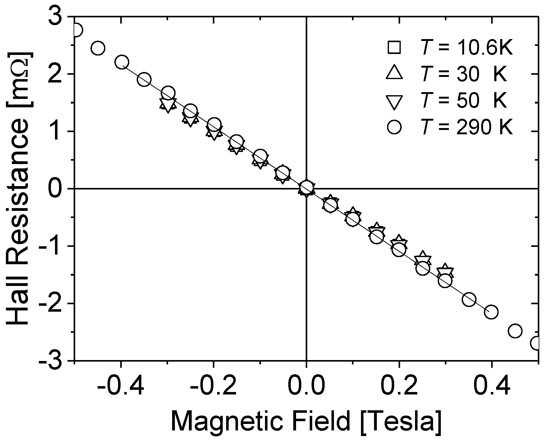
Figure 1 presents the results of the Hall Effect (Hall voltage
VH) measurements as a function of magnetic field at different temperatures for sample H1. The Hall resistance
R =
VH/
Is vs.
B dependences at
T = 10.6 K,
T = 30 K,
T = 50 K and at room temperature (
T = 290 K) are practically identical. This dependence on temperature is characteristic for highly doped material [
23] and indicated that for the all samples under study; the conduction process, in the whole investigated temperature range, is related to only one type of carriers, i.e., the free electrons in the conduction band.
3. Magnetoresistivity as a Function of Temperature
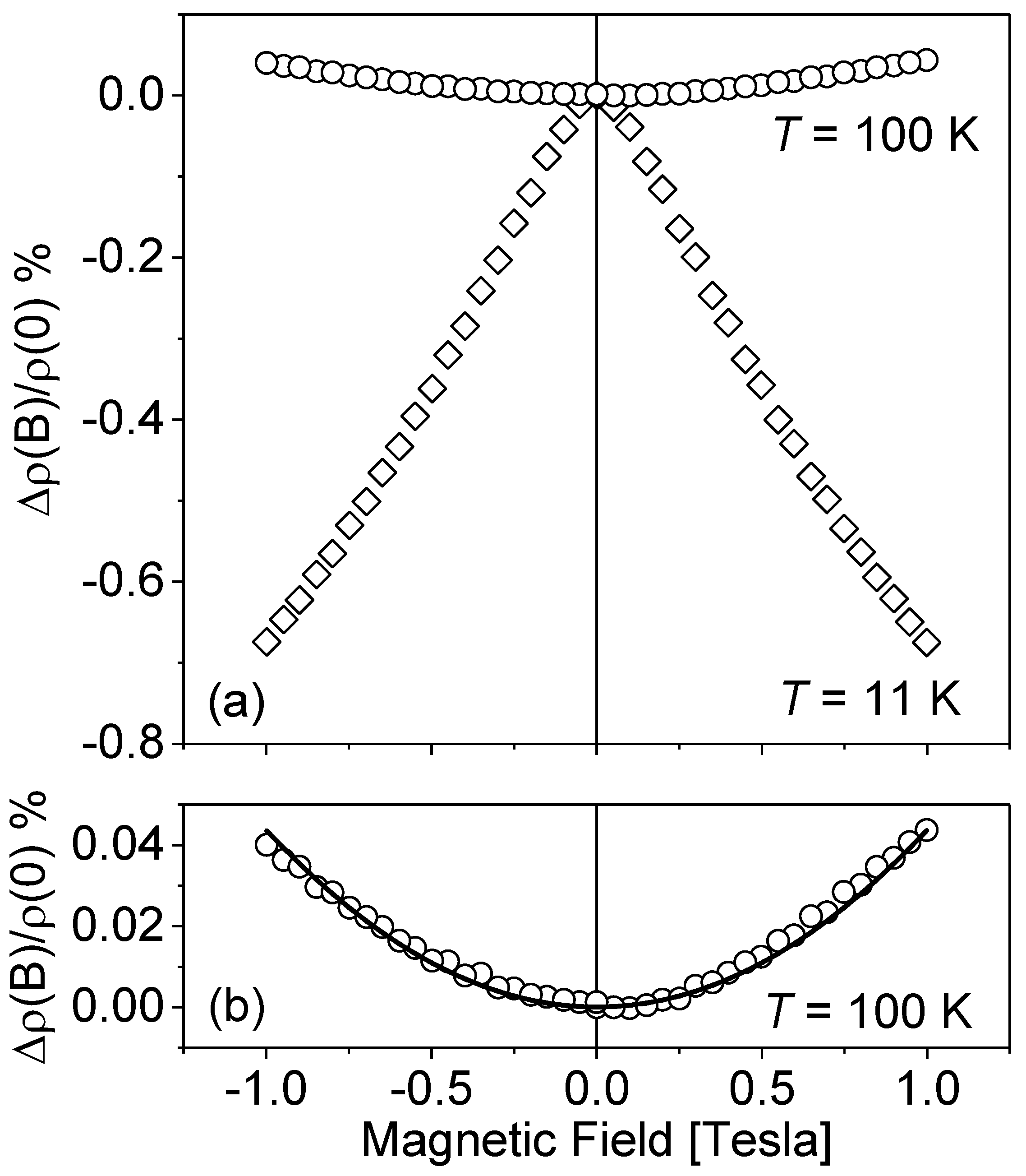
A typical character of resistivity
ρ on the magnetic field dependence is presented in
Figure 2, where the results of
ρ(
B) measurements for sample M5 are plotted at
T = 11 K and 100 K.
The positive magnetoresistivity effect observed at higher temperatures (
T = 100 K) can be analyzed in the frame of classic electron transport phenomena and is given by the following equation [
25]:
where Δ
ρ(
B) =
ρ(
B) −
ρ(
B = 0),
µ is the carrier mobility and
A is the scattering factor related the relaxation time.
The fitting procedure gave the value Aµ²= 4.1 × 10⁻⁴ (T−2). Taking into account the mobility of sample M5 at T = 100 K equal to 175 cm²/Vs, the fitting result corresponds to A = 1.35, which is an expected value between an ionized impurity scattering mode and acoustic phonon modes.
In the low temperatures range, the opposite effect of decreasing resistance as a function of the magnetic field is observed. This is assumed to be related to the phenomenon of weak localization and its dependence on temperature is investigated in the following part of the paper. To study this effect, the data should be analyzed using Kawabata’s equations [
26] for conductivity corrections with a magnetic field in a 3D system. At low temperature, one has to distinguish between two different scattering times of the conduction electrons: elastic scattering time
τo and inelastic scattering time
τφ (phase coherence time after which the coherent backscattering disappears). Using these two parameters, Kawabata derived an expression for the variation of the conductivity as a function of magnetic field in the absence of spin-orbit and magnetic interactions. Depending on the parameter
δ defined as:
with
l being the cyclotron length and
λ,
λε elastic and inelastic mean free path, respectively, he proposed two possible types of behavior of Δ
σ(
B,
T) [
10]:
If
δ << 1: Δ
σ is independent of the parameters characterizing the system and can be expressed by the universal formula:
If
δ >> 1: Δ
σ it is done by a parabolic dependence on
B:
In the above equations,
σo is the conductivity in the absence of magnetic field,
e is the electron charge,
m*—the carrier effective mass (here
m* = 0.22
mo), and ℏ,
π have their usual meanings. In the case where Equation (4) may be applied, the experimental results can be analyzed treating the phasing coherence time τ
φ as the fitting parameter. The experimentally observed low-temperature changes in the conductivity with the magnetic field Δ
σ(
B) =
σ(
B) −
σo for different carrier concentrations are presented in
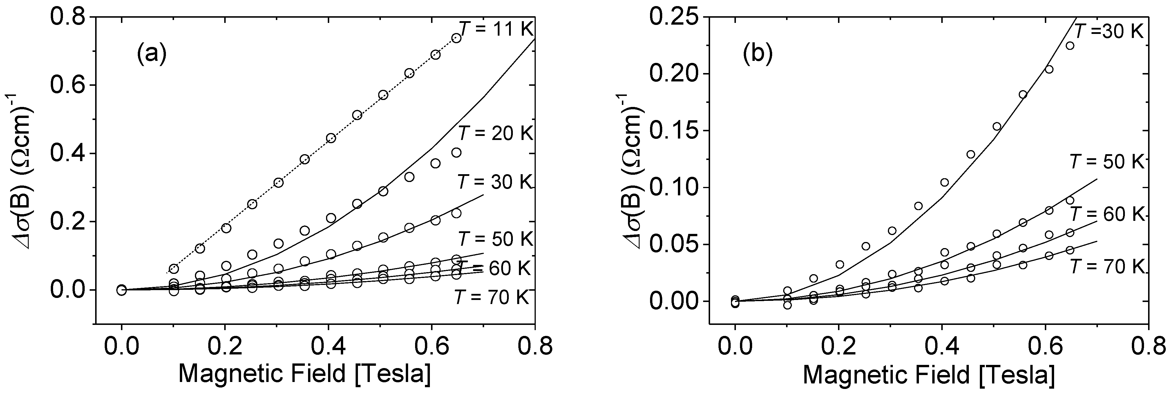
Figure 3. Although the investigated nMR effect is weak (in the best case it does not exceed 1%), the observed trends do not raise any doubts. As can be seen from the figure, the criteria that allow for applying Equations (3) or (4) to describe the conductivity corrections Δ
σ(
B) strongly depend on the carrier concentration in the sample.
In the case of nH > 1 × 1020 cm−3 (sample P6), the experimental dependence Δσ(B) is perfectly described by the universal Equation (3) with the magnetic field dependence~√B. However, as the carrier concentration is lowered, this dependence changes its character so that for nH~1 × 1019 cm−3 the Δσ(B) dependence becomes similar to a parabolic dependence (Δσ~B²) and consequently can be analyzed under Equation (4).
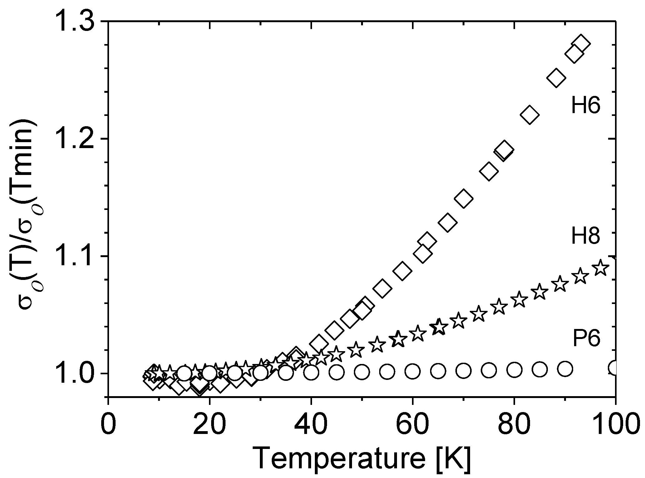
Figure 4 shows, for the discussed three samples, relative changes in their conductivity with temperature. Up to approximately 40 K, the conductivity of all the samples is practically independent of the temperature, while an increase in the conductivity with temperature observed above 40 K appears only for some samples.
The temperature dependence becomes stronger as the concentration of carriers in the sample decreases. As a consequence of the tendency shown in
Figure 3, even if the nMR effect was observed in all samples under study, only for some of them was it possible to evaluate the phasing coherence time τ
φ. For these samples, the magnetoresistance data vs. magnetic field were fitted using Kawabata’s Equation (4), treating the phasing coherence time as the fitting parameter. As an example, Δ
σ(
B) for sample M4 with carrier concentration
nH = 6.9 × 10
19 cm
−3 is presented in
Figure 5. While the results at low temperature do not allow for the fitting of the parabolic dependence of Δ
σ(
B) (Equation (4)), this condition is met by increasing the temperature.
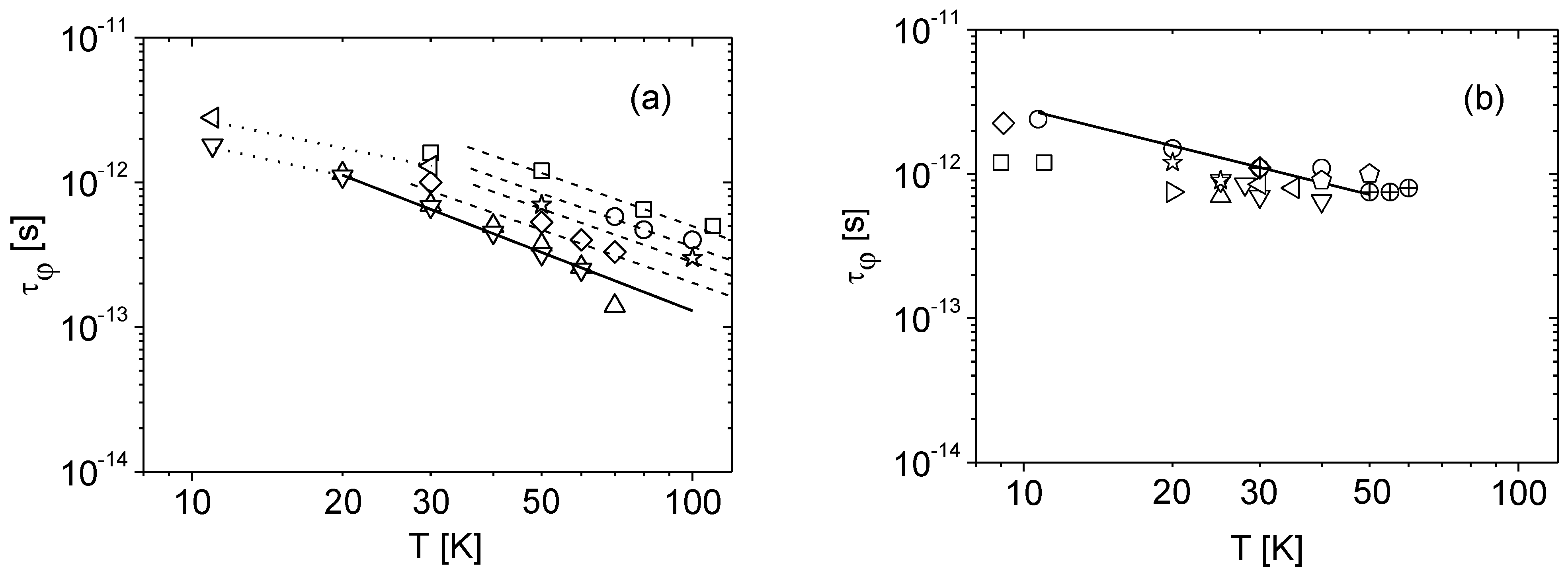
The phasing coherence time dependence on temperature τ
φ(
T) determined this way for several samples are presented in
Figure 6. In
Figure 6a are presented the results for MOVPE, PAMBE, and HVPE samples. In the temperature range
T > 30 K, the best power-law fit of this set of data is of the form:
where G value is characteristic of each sample.
For
T < 30 K, the results for samples H1 and M2 suggest a much weaker dependence on temperature
τφ(
T)∝
T−0.85. The results for Am and MFS samples are presented in
Figure 6b. For these samples the phasing coherence time
τφ could be determined at a lower temperature range
T ≤ 40 K and its temperature dependence can be described by:
with the exponential term consistent with the results in
Figure 6a for the same, lower temperature range.
It should be noted that in the case of the of Si dopant, the phasing coherence time τφ was determined only for one sample (P15) and in the highest temperature range T > 60 K. This may indicate that the surrounding of the Si dopant is different than in the case of Ge or O doping.
The power-law character of temperature variations of the inelastic scattering time
τφ(
T) ∝
T–p allows for identifying the scattering mechanism dominating in the sample. The electron-phonon scattering τ
e-ph and the electron-electron scattering
τe-e are the two main mechanisms responsible for phase-breaking [
13]. In the case of the electron–phonon interaction, the standard theoretical concept scales
τe-ph with temperature as
T−3. In the presence of strong impurity scattering, however, the situation is less straightforward and different values of the exponent of temperature
p, ranging from
p = 2 to
p = 4, have been predicted. In particular, the
T−2 dependence of the relaxation rate is widely observed in experiments [
13]. As can be seen in
Figure 6, the best power-law fit of the experimental results correspond to
τφ ∝
T−1.34. This value of the temperature exponent is significantly lower than (
p ≈ 2÷4) established for the electron–phonon interaction. However, this exponent value is close to
τe-e ∝
T−3/2, the formula for electron–electron interaction in the case of heavily doped material. This scattering mechanism could also explain the observed decrease of the exponent p as the temperature decreases below 30 K. In this temperature range, the phasing coherence time τ
φ could only be measured in the less doped samples, and according to paper [
27] for 3D systems approaching a metal-insulator transition a weaker temperature dependency
τφ ∝
T−1 can be expected. A similar effect of decreasing of the exponential term with decreasing temperature was also observed for the GaN nanowall network [
16].
However, one should also consider the possibility that this effect is related to the experimentally observed effect at a low temperature ‘saturation’ of the electron dephasing rate [
9]. This is due to the fact that the electron dephasing time
τφ can be written as:
where D is presumed to be constant, independent of temperature, and
τi is the relevant inelastic electron scattering time in question. As is evident from this equation, in the higher temperature range (1/
τi > D) the temperature dependence of τ
φ is controlled by the temperature dependence of
τi, while D determines the saturated value of the dephasing time in the limit of very low temperatures. This effect can be related to the inhomogeneities in the samples, which may be of particular importance near the Mott transition.
4. Conclusions
In this paper, the results of low temperature magnetoresistivity study in n type, heavily doped GaN grown by PAMBE, HVPE, MOVPE, Am and MFS were presented.
In this study, we have found that all the samples, regardless of crystal growth technique or dopant, exhibit negative magnetoresistivity (nMR, Δσ > 0). For a great part of the investigated samples, it was possible to determine the temperature range where the Δσ(B) dependency was approaching the parabolic Δσ ∝ B² and could be analyzed in the frame of the weak localization phenomena model. As a result, for the first time, the phasing coherence time τφ was determined for 3D electron gas in GaN. The determined values are coherent with the results for other 3D semiconductor materials.
Such an extensive occurrence of the phenomenon of nMR is worth stressing. It suggests that this particular phenomenon could be applied for more systematic studies of heavily doped materials with different elements in terms of their surrounding in the lattice. For this purpose, it would be interesting to further study Si-doped GaN for which the nMR effect was observable only for the highest temperatures.
We have performed a quantitative determination of the electronic phase coherence time as a function of temperature. At temperature T > 30 K, the measured dephasing rate τφ ∝ T−1.34 agrees well with that predicted by theories based on electron–electron interactions. This result is very surprising and unexpected because at such high temperatures the role of electron phonons scattering should be significant and even dominant.
In the case of less doped samples and T < 30 K, a weaker temperature dependency τφ ∝ T−0.85 was observed, which can be the signature for 3D systems approaching a metal-insulator transition. To study this phenomenon in more detail, it would be advisable to extend the measurements to the lowest possible temperature range. If it turns out that by lowering the temperature, the relaxation time tends to a constant value, conclusions can be made regarding disorder in the system. Then, the nMR phenomenon could be used to estimate the quality of the material.

 ,
, 


 A8; MFS samples: Ψ F1;
  F2; ⊕F3; ◊
  F4; Solid line: τφ(T) = 2 × 10⁻¹¹ × T−0.85 (s).

