
Electrical and Optical Properties of CaTi1−yFeyO3−δ Perovskite Films as Interlayers for Optoelectronic Applications
 , and
, and
Abstract
:1. Introduction
2. Materials and Methods
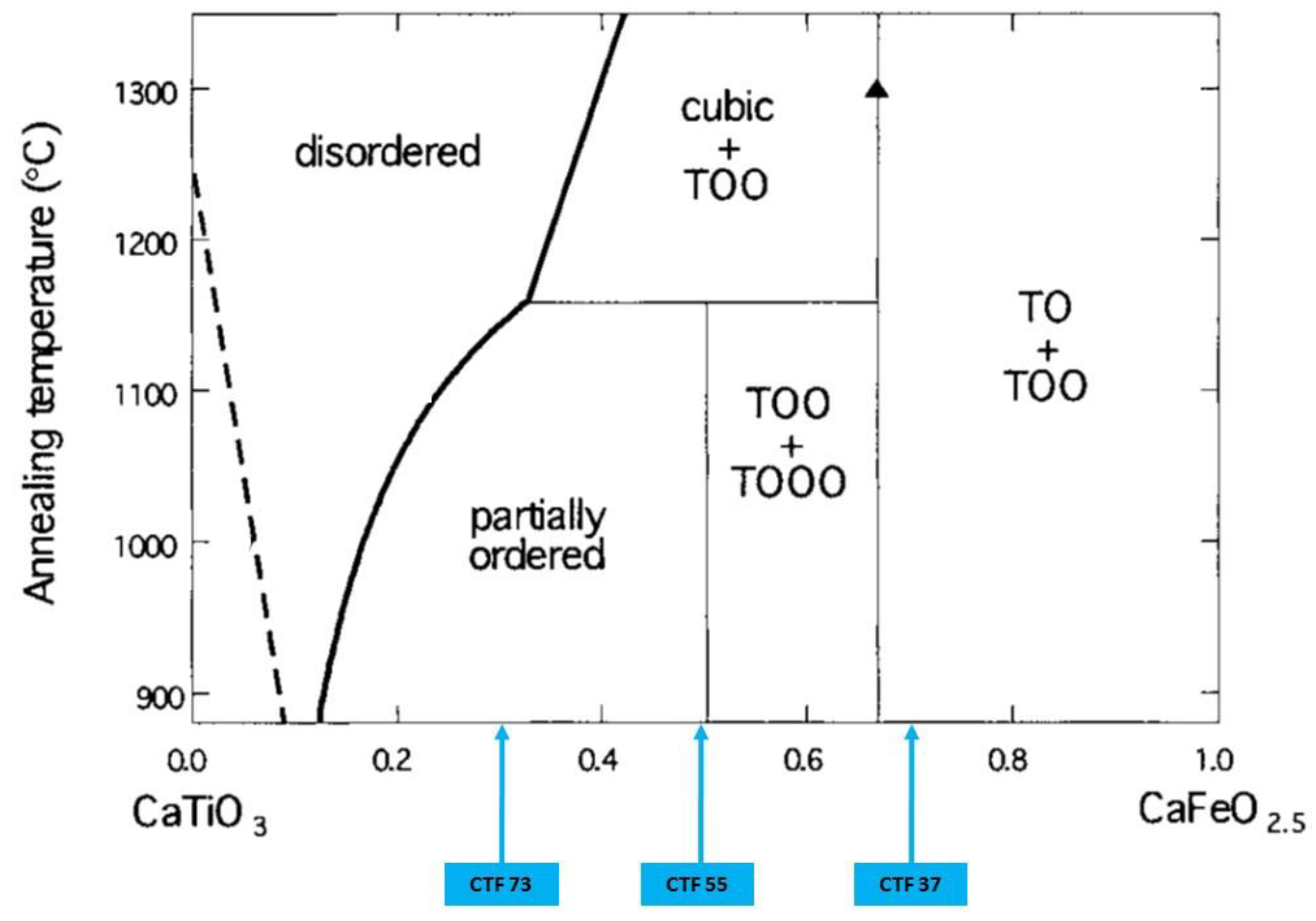
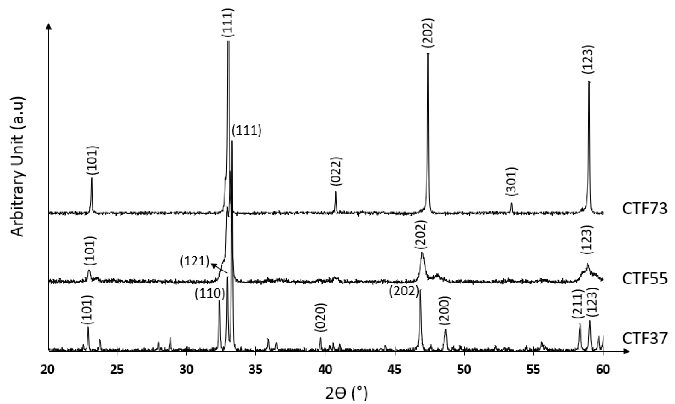
2.1. Synthesis of CaTi1−yFeyO3−δ Perovskite Targets
2.2. Elaboration of CaTi1−yFeyO3−δ Perovskite Films
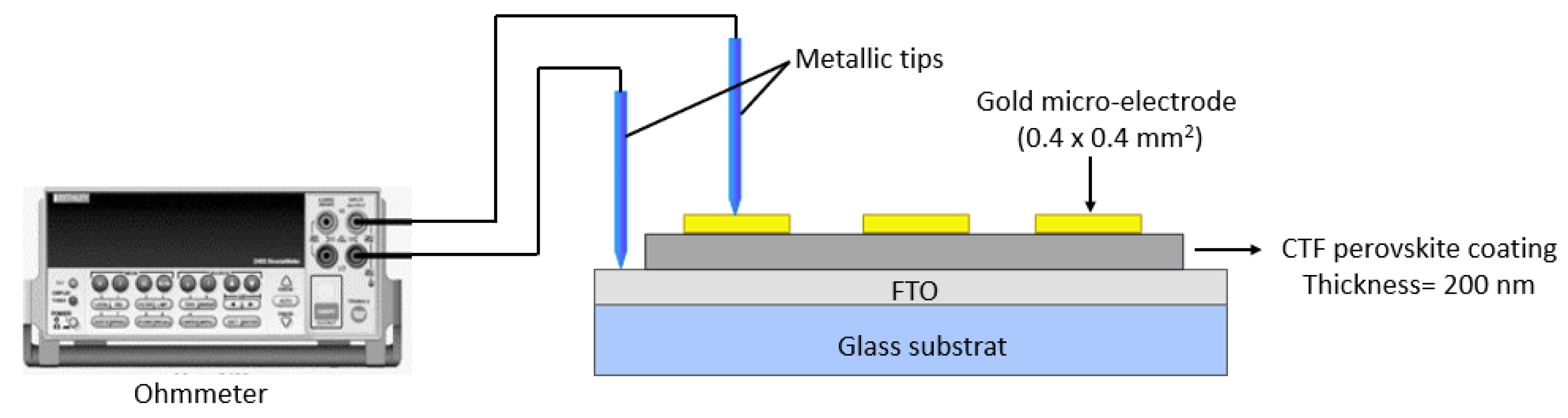
2.3. Electrical Characterizations
2.4. Optical Characterizations
2.5. Surface Potential Measurements
3. Results and Disssion
3.1. Electrical Characterization of CaTi1−yFeyO3−δ Perovskite Pellets
3.2. Characterization of CaTi1−yFeyO3−δ Perovskite Films Deposited by PLD
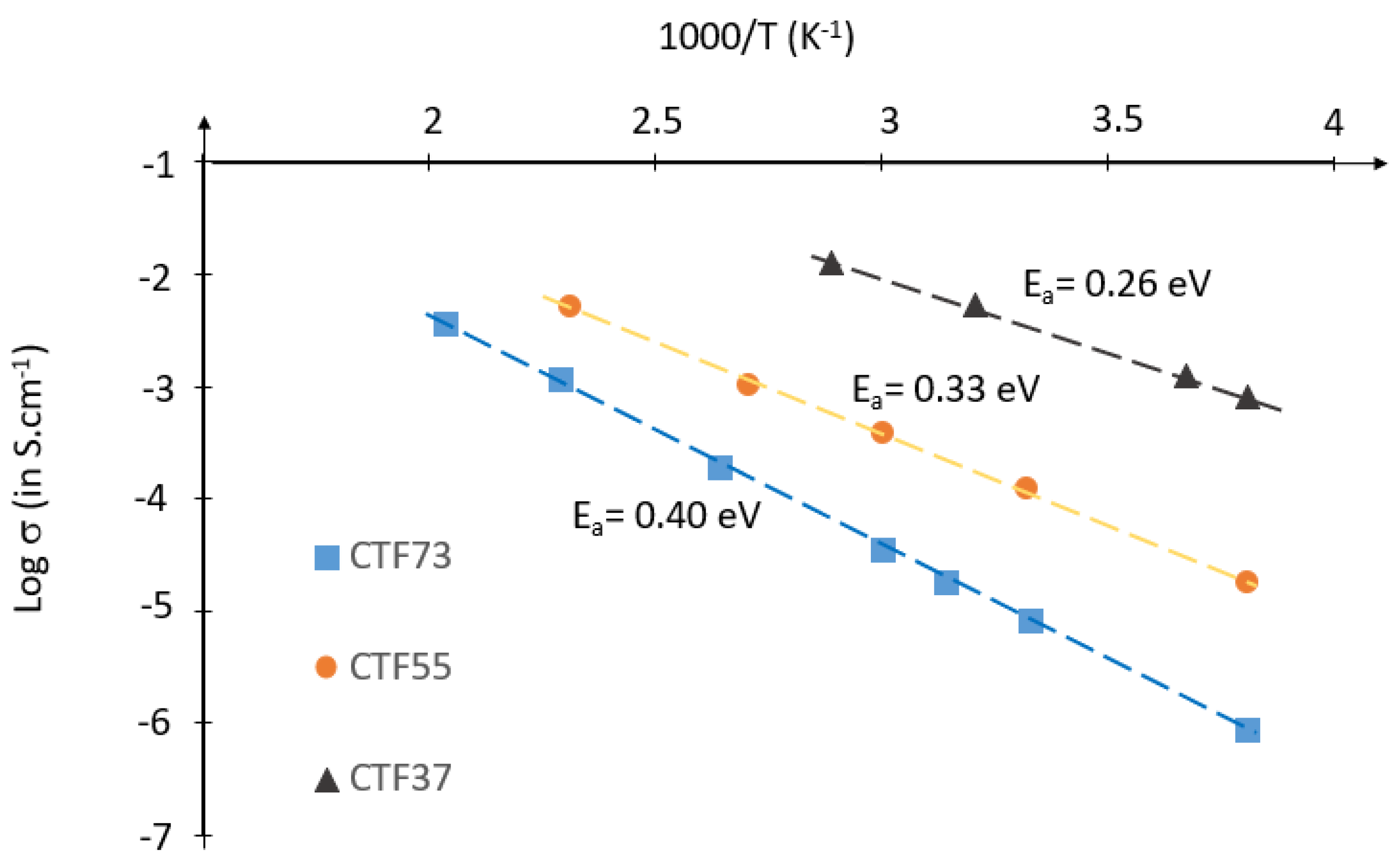
3.2.1. Electrical Characterizations of CaTi1−yFeyO3−δ Perovskite Films
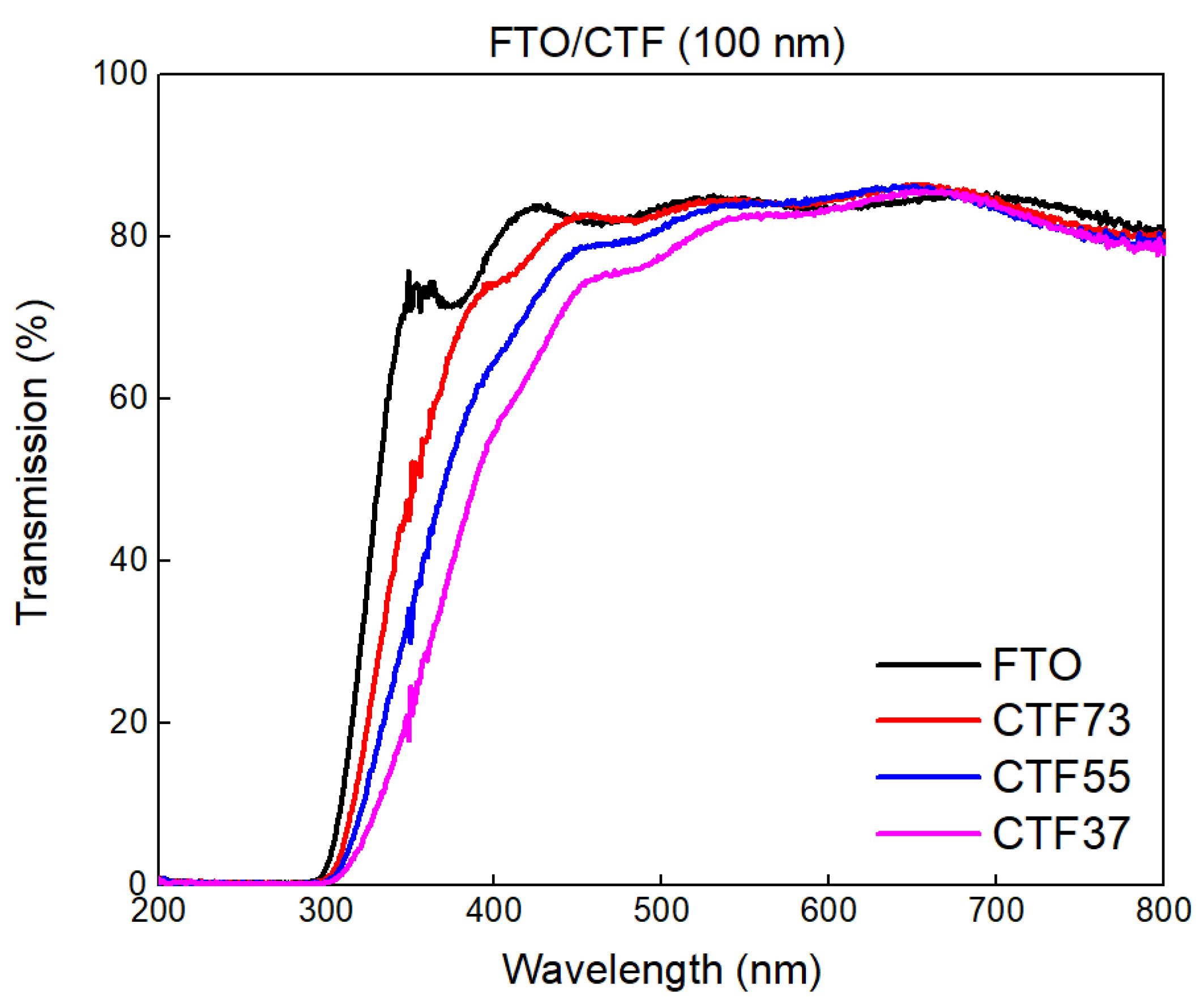
3.2.2. Optical Characterization
4. Conclusions
Supplementary Materials
Author Contributions
Funding
Institutional Review Board Statement
Informed Consent Statement
Data Availability Statement
Conflicts of Interest
References
- Wang, F.; Grinberg, I.; Rappe, A.M. Band gap engineering strategy via polarization rotation in perovskite ferroelectrics. Appl. Phys. Lett. 2014, 104, 152903. [Google Scholar] [CrossRef]
- Borse, P.H.; Lee, J.S.; Kim, H.G. Theoretical band energetics of Ba(M0.5Sn0.5)O3 for solar photoactive applications. J. Appl. Phys. 2006, 100, 124915. [Google Scholar] [CrossRef]
- Brenner, T.M.; Egger, D.A.; Kronik, L.G.; Hodes, G.; Cahen, D. Hybrid organic–inorganic perovskites: Low-cost semiconductors with intriguing charge-transport properties. Nat. Rev. Mater. 2016, 1, 15007. [Google Scholar] [CrossRef]
- Orlovskaya, N.; Browning, N. Mixed Ionics Electronics Conducting Perovskites for Advanced Energy Systems; Nato Sciences Series II: Mathematics, Physics and Chemistry; Orlovskaya, N., Browning, N., Eds.; Springer: Berlin/Heidelberg, Germany, 2003; p. 173. [Google Scholar]
- Chen, H.; Umezawa, N. Artificial layered perovskite oxides A(B0.5B′0.5)O3 as potential solar energy conversion materials. J. Appl. Phys. 2015, 117, 055106. [Google Scholar] [CrossRef]
- Geffroy, P.-M.; Vedraine, S.; Dumas-Bouchiat, F.; Gheno, A.; Rossignol, F.; Marchet, P.; Boucle, J.; Ratier, B. Electrical and optical properties of La1−xAxFe1−yByO3−δ perovskite films (with A = Sr and Ca, and B = Co, Ga, Ti) for potential photovoltaic applications. J. Phys. Chem. C 2016, 120, 28583–28590. [Google Scholar] [CrossRef]
- Becerro, A.I.; Redfern, S.A.T.; Carpenter, M.A.; Knight, K.S.; Seifert, F. Displacive phase transitions in and strain analysis of Fe-Doped CaTiO3 Perovskites at high temperatures by neutron diffraction. J. Solid-State Chem. 2002, 167, 459–471. [Google Scholar] [CrossRef]
- Van Den Bossche, M. Oxygen Vacancy Ordering in Iron-Doped Calcium Titanate. Ph.D. Thesis, University of Tweente, Enschede, The Netherlands, 2005. [Google Scholar]
- Figueiredo, F.M.; Waerenborgh, J.; Kharton, V.V.; Näfe, H.; Frade, J.R. On the relationships between structure, oxygen stoichiometry and ionic conductivity of CaTi1−xFexO3−δ (x = 0.05, 0.20, 0.40, 0.60). Solid State Ion. 2003, 156, 371–381. [Google Scholar] [CrossRef]
- Dunyushkina, L.A.; Gorelov, V.P. High temperature electrical behavior of CaTi1−xFexO3−δ (x = 0–0.5) Oxygen-ion, electronic and proton conductivity. Solid State Ion. 2013, 253, 169–174. [Google Scholar] [CrossRef]
- Salles, C.; Bassat, J.M.; Fouletier, J.; Marinha, D.; Steil, M.-C. Oxygen pressure dependence of the ionic conductivity of iron-doped calcium titanate. Solid State Ion. 2018, 324, 103–108. [Google Scholar] [CrossRef]
- McCammon, C.A.; Becerro, A.I.; Langenhorst, F.; Angel, R.J.; Marion, S.; Seifert, F. Short-range ordering of oxygen vacancies in CaFexTi1−xO3−x/2 perovskites (0 < x < 0.4). J. Phys. Condens. Matter 2000, 12, 2969–2984. [Google Scholar]
- Castelli, I.E.; Thygesen, K.S.; Jacobsen, K.W. Calculated optical absorption of different perovskite phases. J. Mater. Chem. A 2015, 3, 12343–12349. [Google Scholar] [CrossRef]
- Kanhere, P.; Chen, Z. A review on visible light active perovskite-based photocatalysts. Molecules 2014, 19, 19995–20022. [Google Scholar] [CrossRef] [PubMed]
- Sindhu, S.; Sanghi, S.; Agarwal, A.; Seth, V.P.; Kishore, N. Effect of Bi2O3 content on the optical band gap, density, and electrical conductivity of MO·Bi2O3·B2O3 (M = Ba, Sr) glasses. Mater. Chem. Phys. 2005, 90, 83–89. [Google Scholar] [CrossRef]
- Docamo, P.; Hey, A.; Guldin, S.; Gunning, R.; Steiner, U.; Snaith, H.J. Pore filling of Spiro-OMeTAD in solid-state dye-sensitized solar cells determined via optical reflectometry. Adv. Funct. Mater. 2012, 22, 5010. [Google Scholar] [CrossRef]
- Löper, P.; Stuckelberger, M.; Niesen, B.; Werner, J.; Filipic, M.; Moon, S.-J.; Yum, J.-H.; Topic, M.; De Wolf, S.; Ballif, C. Complex refractive index spectra of CH3NH3PbI3 Perovskite thin films determined by spectroscopic ellipsometry and spectrophotometry. J. Phys. Chem. Lett. 2015, 6, 66–71. [Google Scholar] [CrossRef]
- Gheno, A.; Trigaud, T.; Bouclé, J.; Audebert, P.; Ratier, B.; Vedraine, S. Stability assessments on luminescent down-shifting molecules for UV-protection of perovskite solar cells. Opt. Mater. 2018, 75, 781–786. [Google Scholar] [CrossRef]
- Zhou, H.; Chen, Q.; Li, G.; Luo, S.; Song, T.-B.; Duan, H.-S.; Hong, Z.; You, J.; Liu, Y.; Yang, Y. Interface engineering of highly efficient perovskite solar cells. Science 2014, 345, 542–546. [Google Scholar] [CrossRef]
- Luo, S.; Daoud, W.A. Recent progress in organic–inorganic halide perovskite solar cells: Mechanisms and material design. J. Mater. Chem. A 2015, 3, 8992–9010. [Google Scholar] [CrossRef]
- Ichikawa, M.; Amagai, J.; Horiba, Y.; Koyama, T.; Taniguchi, Y. Dynamic turn-on behavior of organic light-emitting devices with different work function cathode metals under fast pulse excitation. J. Appl. Phys. 2003, 94, 7796–7800. [Google Scholar] [CrossRef]
- Gheno, A.; Vedraine, S.; Ratier, B.; Bouclé, J. π-conjugated materials as the hole-transporting layer in perovskite solar cells. Metals 2016, 6, 21. [Google Scholar] [CrossRef]
- Huang, Y.; Gheno, A.; Rolland, A.; Pedesseau, L.; Vedraine, S.; Durand, O.; Bouclé, J.; Connolly, J.P.; Etgar, L.; Even, J. A new approach to modelling Kelvin probe force microscopy of hetero-structures in the dark and under illumination. Opt. Quantum Electron. 2018, 50, 41. [Google Scholar] [CrossRef]
- Belchi, R.; Habert, A.; Foy, E.; Gheno, A.; Vedraine, S.; Antony, R.; Ratier, B.; Bouclé, J.; Herlin-Boime, N. One-step synthesis of TiO2/graphene nanocomposites by laser pyrolysis with well-controlled properties and application in perovskite solar cells. ACS Omega 2019, 4, 11906–11913. [Google Scholar] [CrossRef] [PubMed]
- Al-Zohbi, F.; Jouane, Y.; Benhattab, S.; Faure-Vincent, J.; Tran-Van, F.; Vedraine, S.; Bouclé, J.; Berton, N.; Schmaltz, B. Simple carbazole-based hole transporting materials with fused benzene ring substituents for efficient perovskite solar cells. New J. Chem. 2019, 43, 12211. [Google Scholar] [CrossRef]


| Materials | Acronym | Sintering Conditions | Density of Starting Powders (Pycnometer, g·cm−3) | Relative Density of Sintered Pellets |
|---|---|---|---|---|
| CaTi0.7Fe0.3O3−δ | CTF73 | 1400 °C, 6 h, air | 3.92 | >98% |
| CaTi0.5Fe0.5O3−δ | CTF55 | 1400 °C, 6 h, air | 3.85 | >98% |
| CaTi0.3Fe0.7O3−δ | CTF37 | 1400 °C, 6 h, air | 3.83 | >98% |
| Compositions | CTF73 Perovskite | CTF55 Perovskite | CTF37 Perovskite | ||
|---|---|---|---|---|---|
| Electrical conductivity (S·cm−1) | Pellets | 8.7·10−7 | 1.8·10−5 | 8·10−4 | |
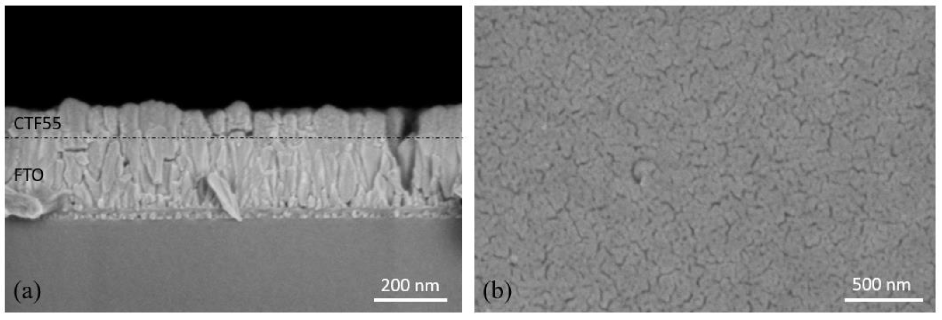
| PLD coating before annealing | Close to 200 nm (in thickness) | 2·10−10 | 5·10−10 | 8·10−10 | |
| PLD coating after annealing under air at 500 °C during 4 h | Close to 200 nm (in thickness) | 7·10−9 | 4·10−7 | 1.3·10−8 | |
| Materials | Acronym | Work function (eV) | Gap (eV) |
|---|---|---|---|
| CaTi0.7Fe0.3O3−δ | CTF73 | 5 | 3.2 (indirect) |
| CaTi0.5Fe0.5O3−δ | CTF55 | 5 | 3.4 (indirect) |
| CaTi0.3Fe0.7O3−δ | CTF37 | 5 | 3.5 (indirect) |
Publisher’s Note: MDPI stays neutral with regard to jurisdictional claims in published maps and institutional affiliations. |
© 2022 by the authors. Licensee MDPI, Basel, Switzerland. This article is an open access article distributed under the terms and conditions of the Creative Commons Attribution (CC BY) license (https://creativecommons.org/licenses/by/4.0/).
Share and Cite
Yildirim, C.; Devoize, F.; Geffroy, P.-M.; Dumas-Bouchiat, F.; Bouclé, J.; Vedraine, S. Electrical and Optical Properties of CaTi1−yFeyO3−δ Perovskite Films as Interlayers for Optoelectronic Applications. Materials 2022, 15, 6533. https://doi.org/10.3390/ma15196533
Yildirim C, Devoize F, Geffroy P-M, Dumas-Bouchiat F, Bouclé J, Vedraine S. Electrical and Optical Properties of CaTi1−yFeyO3−δ Perovskite Films as Interlayers for Optoelectronic Applications. Materials. 2022; 15(19):6533. https://doi.org/10.3390/ma15196533
Chicago/Turabian StyleYildirim, Ceren, Fabien Devoize, Pierre-Marie Geffroy, Frédéric Dumas-Bouchiat, Johann Bouclé, and Sylvain Vedraine. 2022. "Electrical and Optical Properties of CaTi1−yFeyO3−δ Perovskite Films as Interlayers for Optoelectronic Applications" Materials 15, no. 19: 6533. https://doi.org/10.3390/ma15196533