
Stoichiometry and Morphology Analysis of Thermally Deposited V2O5−x Thin Films for Si/V2O5−x Heterojunction Solar Cell Applications

 , , and
Abstract
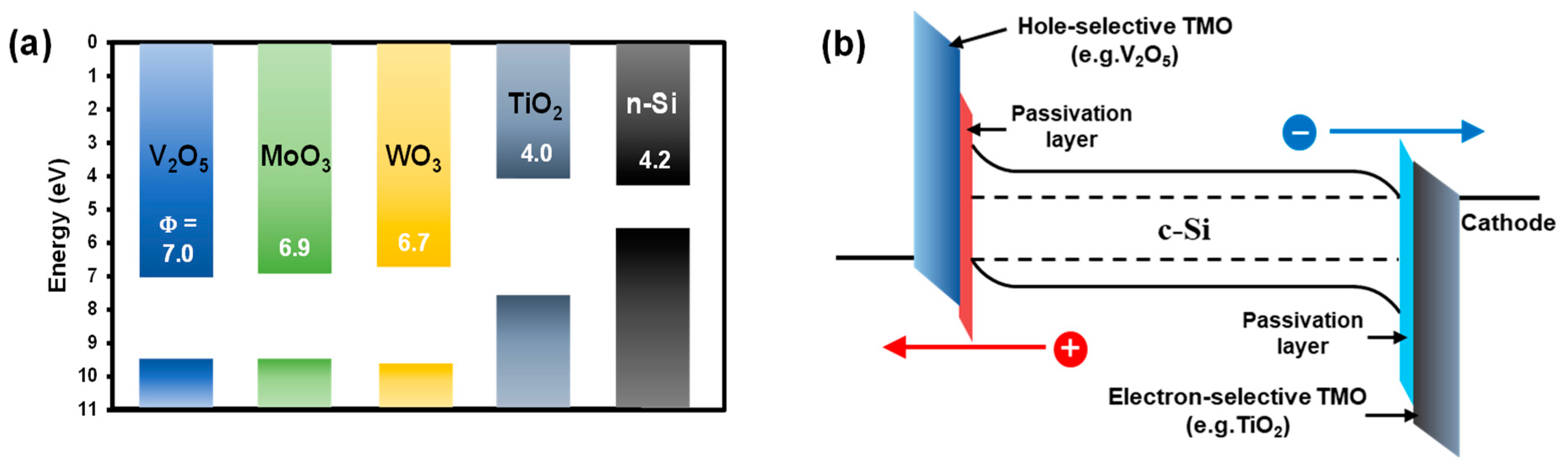
:1. Introduction
2. Experimental
2.1. Materials and Sample Preparation
2.2. Characterization
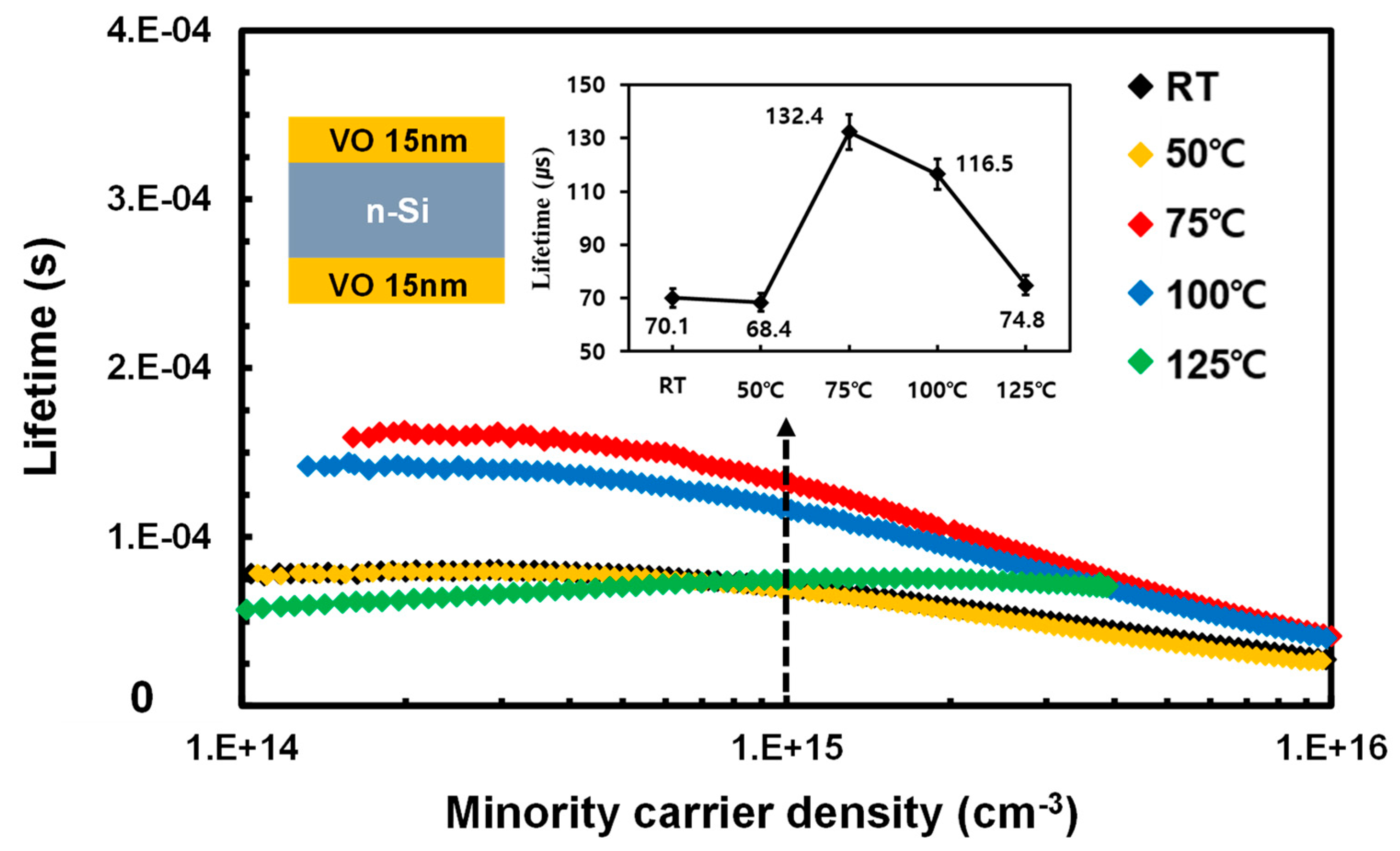
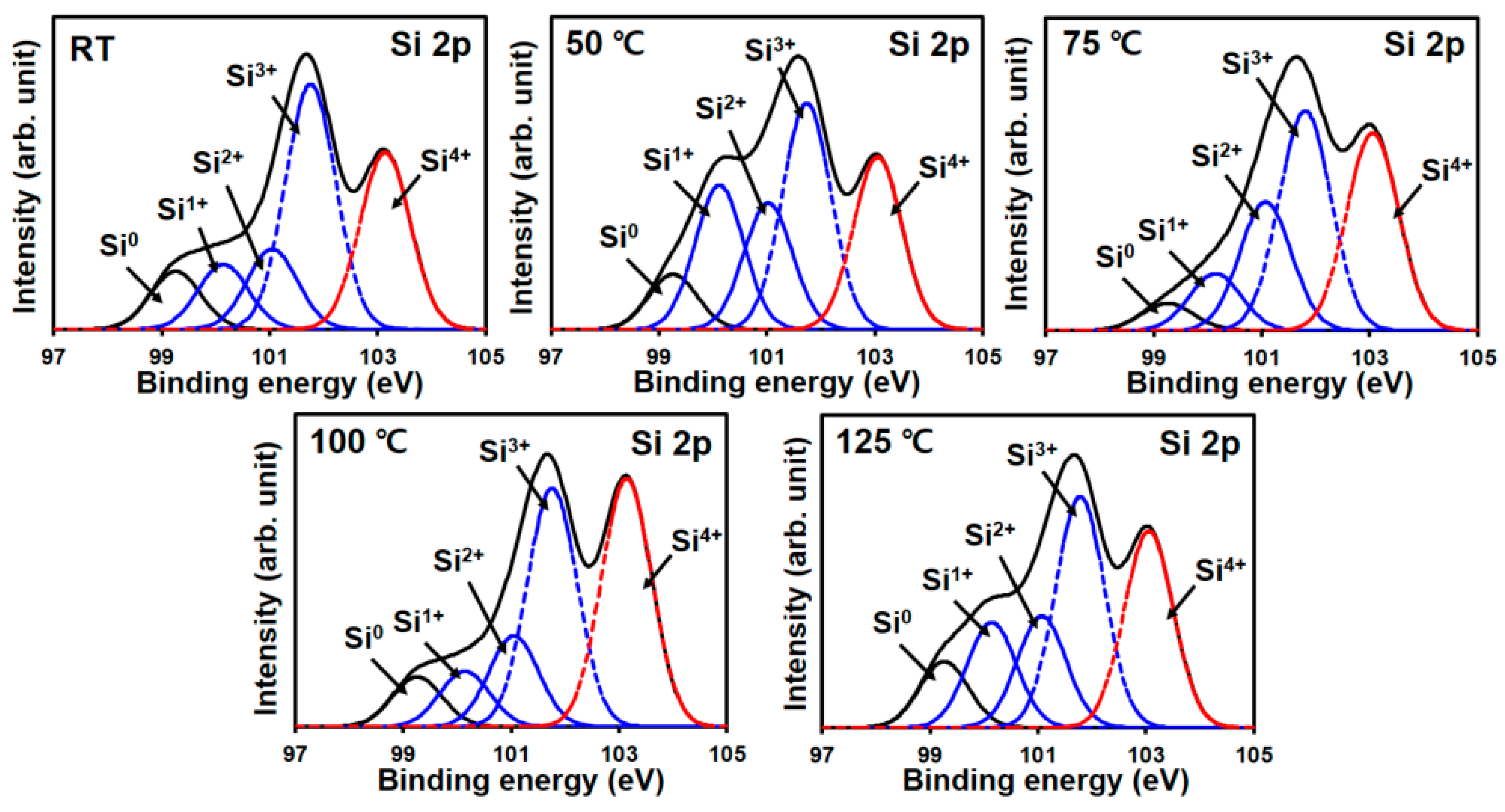
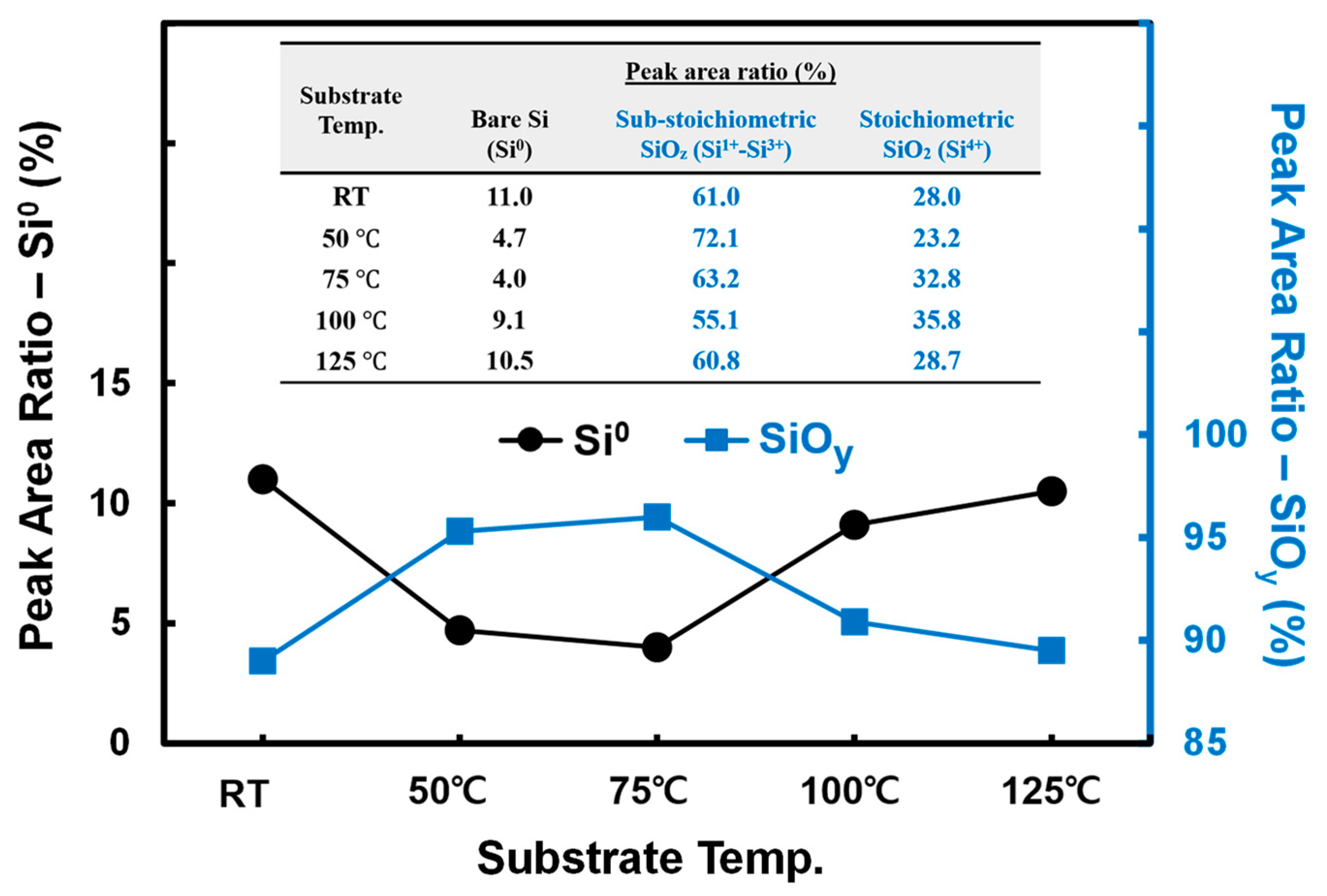
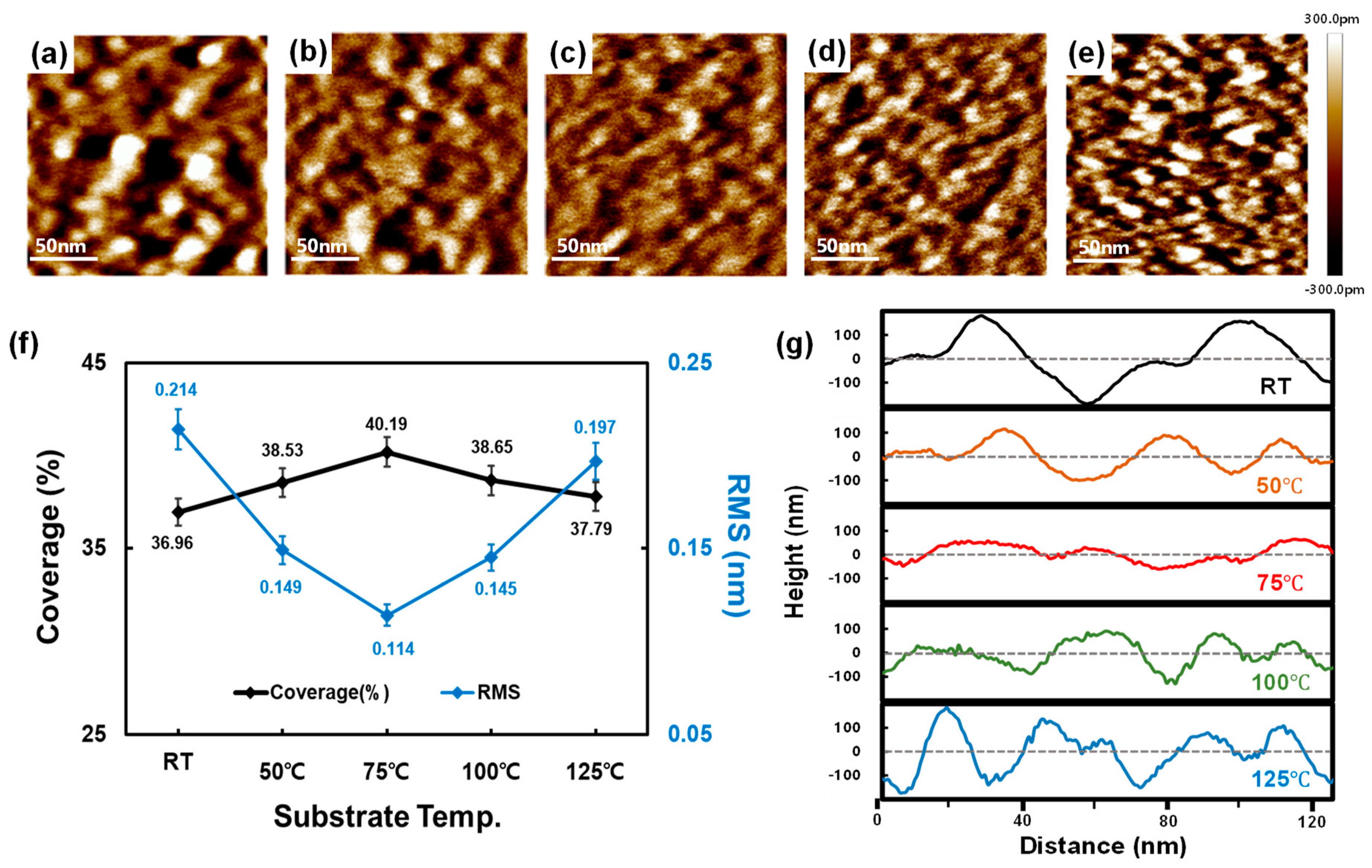
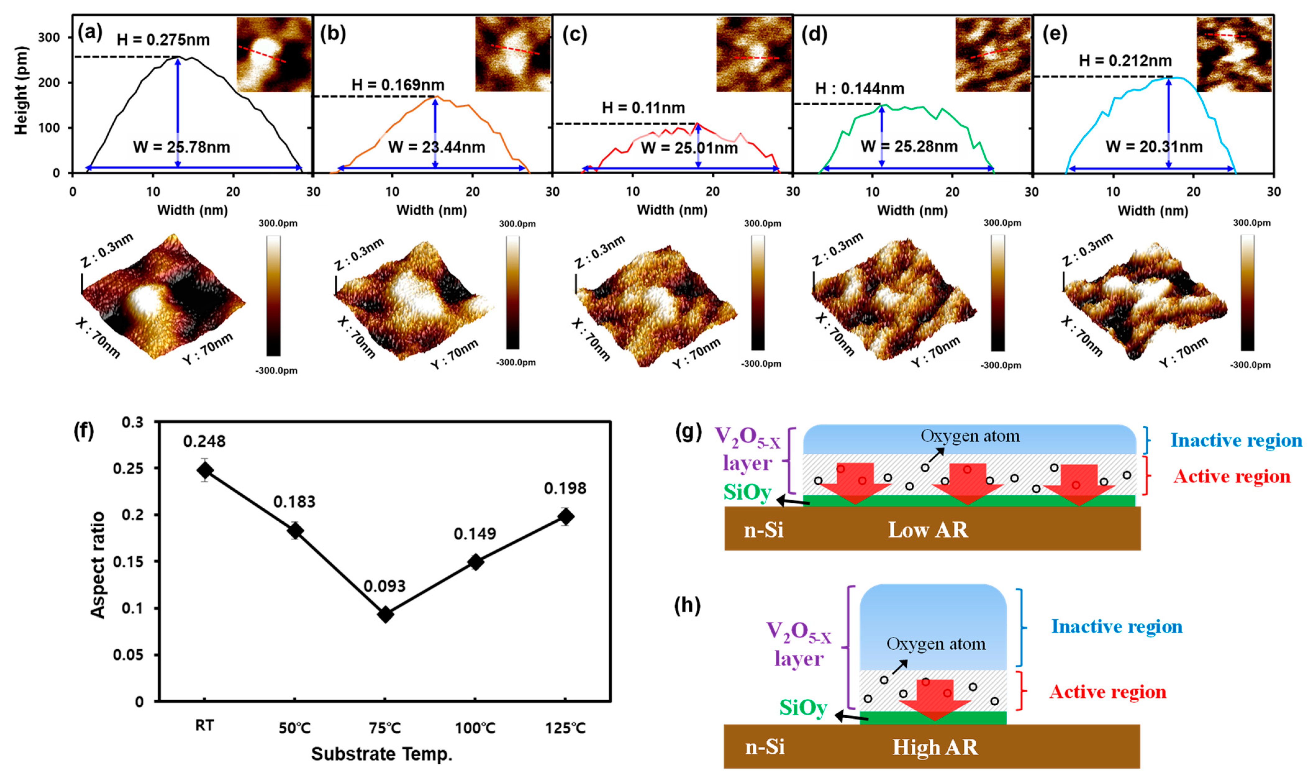
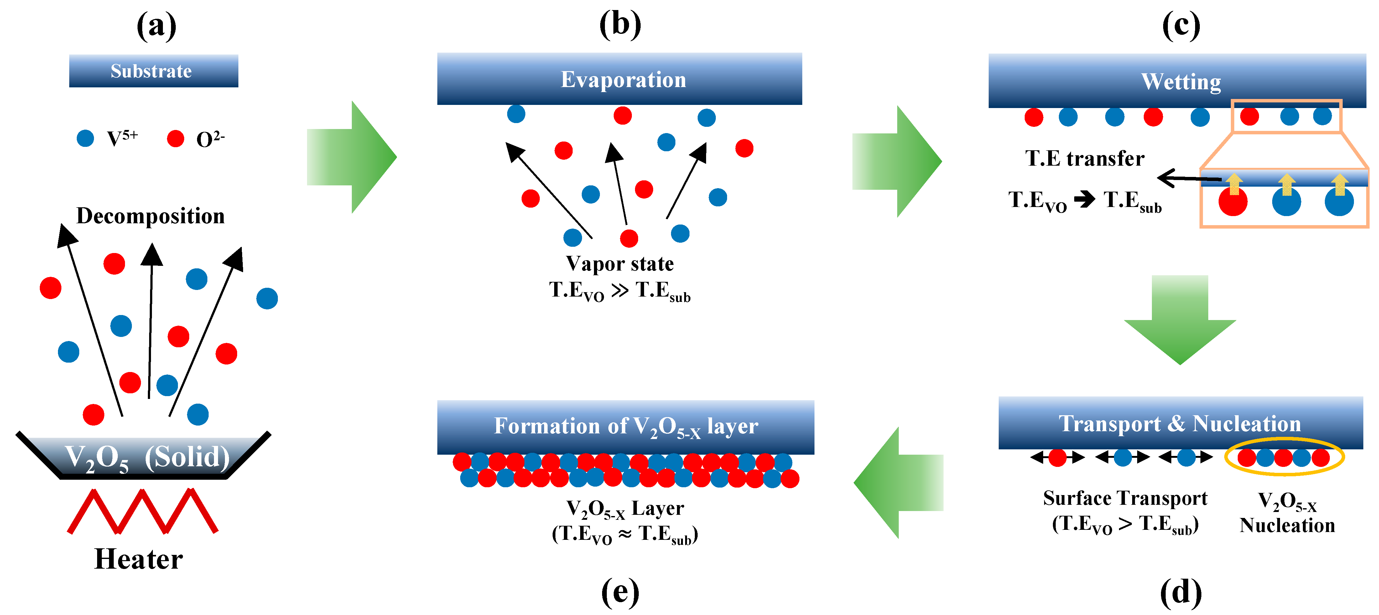
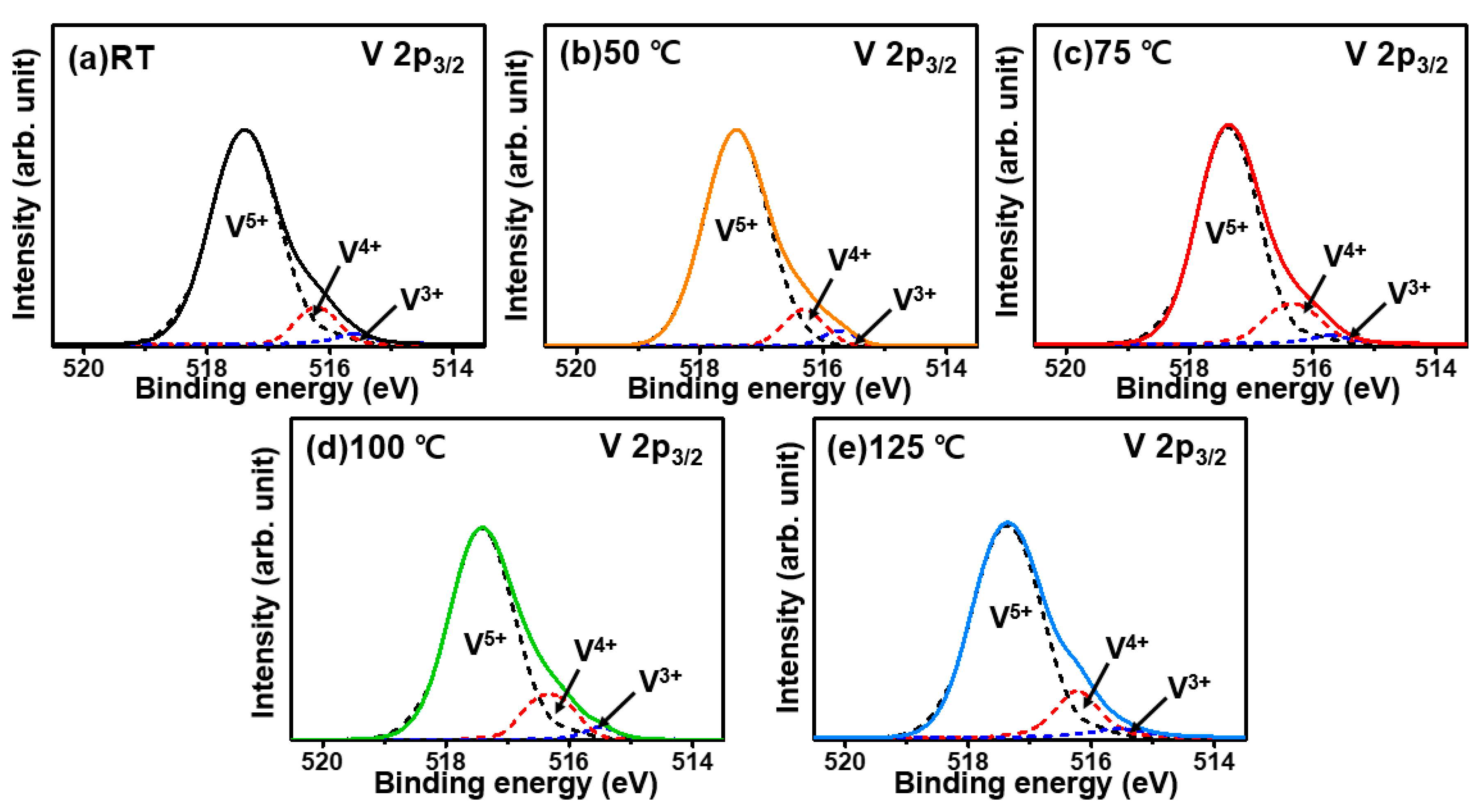
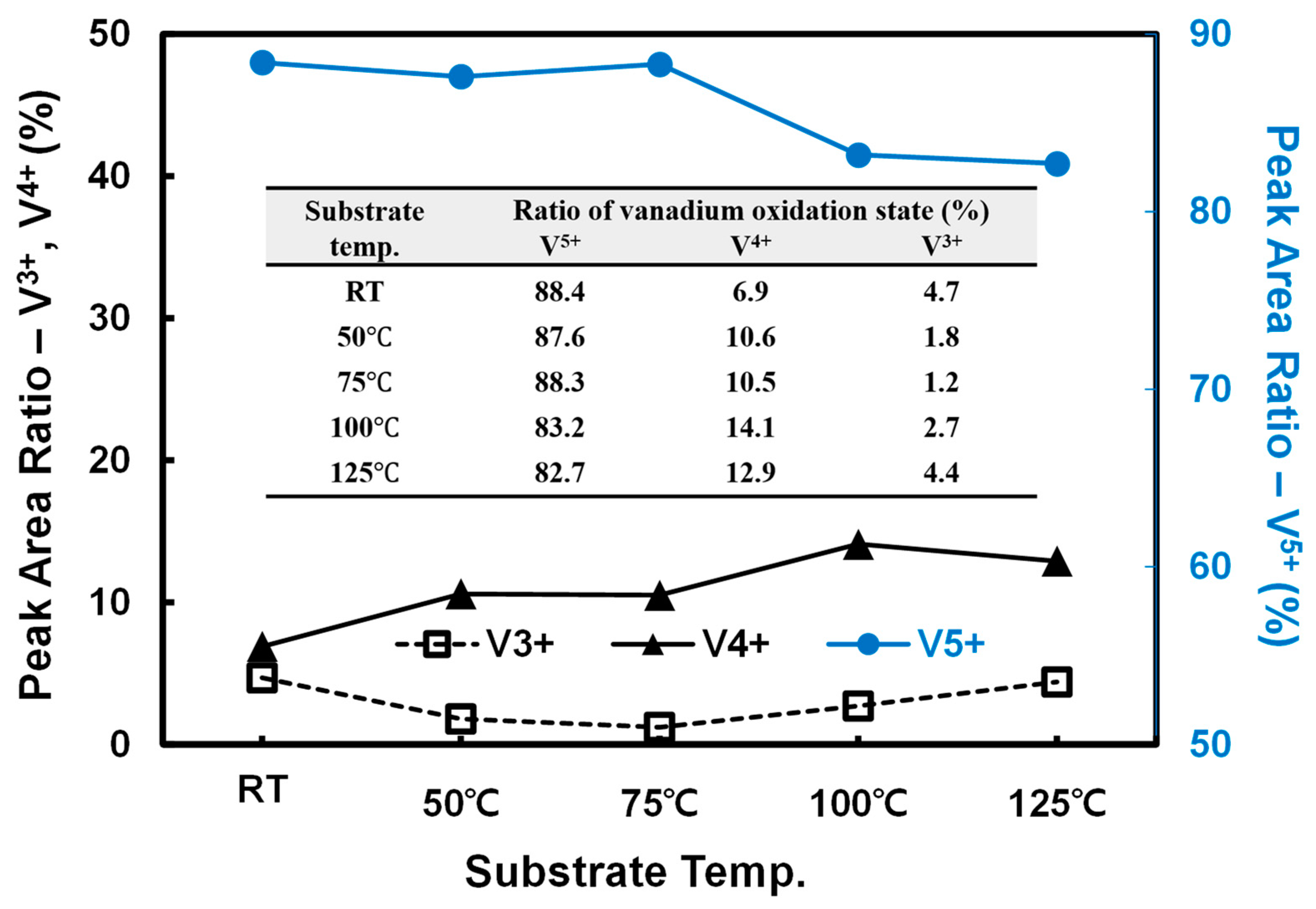
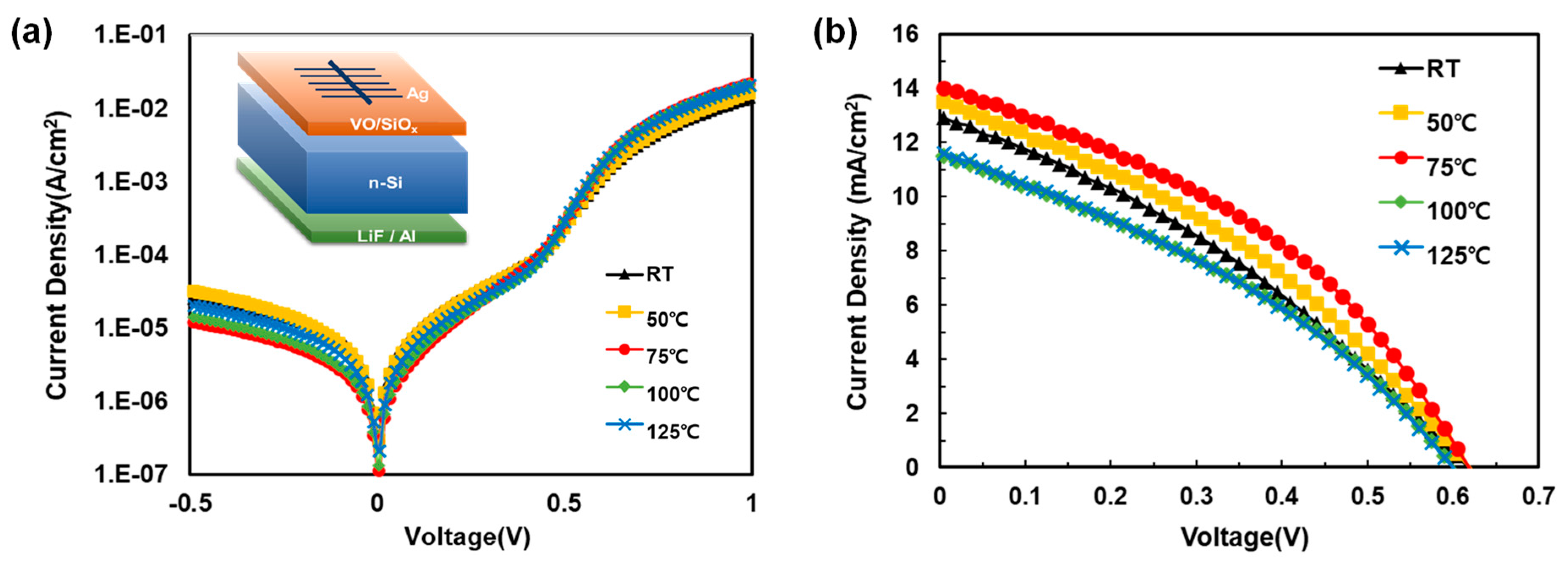
3. Results and Discussion
4. Conclusions
Supplementary Materials
Author Contributions
Funding
Conflicts of Interest
References
- Louwen, A.; Van Sark, W.; Schropp, R.; Faaij, A. A cost roadmap for silicon heterojunction solar cells. Sol. Energy Mater. Sol. Cells 2016, 147, 295–314. [Google Scholar] [CrossRef] [Green Version]
- Bermel, P.; Luo, C.; Zeng, L.; Kimerling, L.C.; Joannopoulos, J.D. Improving thin-film crystalline silicon solar cell efficiencies with photonic crystals. Opt. Express 2007, 15, 16986–17000. [Google Scholar] [CrossRef] [PubMed]
- Chong, T.K.; Wilson, J.; Mokkapati, S.; Catchpole, K.R. Optimal wavelength scale diffraction gratings for light trapping in solar cells. J. Opt. 2012, 14, 024012. [Google Scholar] [CrossRef] [Green Version]
- Hwang, I.; Jeong, Y.; Shiratori, Y.; Park, J.; Miyajima, S.; Yoon, I.; Seo, K. Effective Photon Management of Non-Surface-Textured Flexible Thin Crystalline Silicon Solar Cells. Cell Rep. Phys. Sci. 2020, 1, 100242. [Google Scholar]
- Zhang, Y.; Stokes, N.; Jia, B.; Fan, S.; Gu, M. Towards ultra-thin plasmonic silicon wafer solar cells with minimized efficiency loss. Sci. Rep. 2014, 4, 4393. [Google Scholar] [CrossRef]
- Werner, J.; Niesen, B.; Ballif, C. Perovskite/silicon tandem solar cells: Marriage of convenience or true love story?—An overview. Adv. Mater. Interfaces 2018, 5, 1700731. [Google Scholar] [CrossRef]
- Wu, Q.-H.; Thissen, A.; Jaegermann, W.; Liu, M. Photoelectron spectroscopy study of oxygen vacancy on vanadium oxides surface. Appl. Surf. Sci. 2004, 236, 473–478. [Google Scholar] [CrossRef]
- Weingarten, M.; Zweipfennig, T.; Vescan, A.; Kalisch, H. Low-temperature processed hybrid organic/silicon solar cells with power conversion efficiency up to 6.5%. MRS Online Proc. Libr. Arch. 2015, 1771, 201–206. [Google Scholar] [CrossRef]
- Thomas, J.P.; Leung, K.T. Defect-minimized PEDOT: PSS/planar-Si solar cell with very high efficiency. Adv. Funct. Mater. 2014, 24, 4978–4985. [Google Scholar] [CrossRef]
- Hussain, B.; Ebong, A.; Ferguson, I. Zinc oxide as an active n-layer and antireflection coating for silicon based heterojunction solar cell. Sol. Energy Mater. Sol. Cells 2015, 139, 95–100. [Google Scholar] [CrossRef]
- Bivour, M.; Temmler, J.; Steinkemper, H.; Hermle, M. Alternative contact materials for induced junction silicon solar cells. Sol. Energy Mater. Sol. Cells 2015, 142, 34–41. [Google Scholar] [CrossRef]
- Bullock, J.; Yan, D.; Cuevas, A.; Wan, Y.; Samundsett, C. N-and p-typesilicon solar cells with molybdenum oxide hole contacts. Energy Procedia 2015, 77, 446–450. [Google Scholar] [CrossRef] [Green Version]
- Smith, R.P.; Hwang, A.A.-C.; Beetz, T.; Helgren, E. Introduction to semiconductor processing: Fabrication and characterization of pn junction silicon solar cells. Am. J. Phys. 2018, 86, 740–746. [Google Scholar] [CrossRef] [Green Version]
- He, J.; Wang, G.; Qiu, Y.; Tang, Z.; Ye, F.; Zhang, C.; Wang, S.; Cai, L.; Yu, T.; Gao, P. Enabling Transparent-Conductive-Oxide Free Efficient Heterojunction Solar Cells by Flexibly Using Dopant-Free Contact. Adv. Funct. Mater. 2022, 2205901. [Google Scholar] [CrossRef]
- Meyer, J.; Hamwi, S.; Kröger, M.; Kowalsky, W.; Riedl, T.; Kahn, A. Transition metal oxides for organic electronics: Energetics, device physics and applications. Adv. Mater. 2012, 24, 5408–5427. [Google Scholar] [CrossRef]
- Gerling, L.G.; Mahato, S.; Voz, C.; Alcubilla, R.; Puigdollers, J. Characterization of transition metal oxide/silicon heterojunctions for solar cell applications. Appl. Sci. 2015, 5, 695–705. [Google Scholar] [CrossRef] [Green Version]
- Cho, E.-C.; Cho, Y.H.; Yi, J. Research and Development Trend of Carrier Selective Energy Contact Solar Cells. Curr. Photovolt. Res. 2018, 6, 43–48. [Google Scholar]
- Wang, Z.; Li, P.; Liu, Z.; Fan, J.; Qian, X.; He, J.; Peng, S.; He, D.; Li, M.; Gao, P. Hole selective materials and device structures of heterojunction solar cells: Recent assessment and future trends. APL Mater. 2019, 7, 110701. [Google Scholar] [CrossRef] [Green Version]
- Wu, W.; Bao, J.; Jia, X.; Liu, Z.; Cai, L.; Liu, B.; Song, J.; Shen, H. Dopant-free back contact silicon heterojunction solar cells employing transition metal oxide emitters. Phys. Status Solidi (RRL)–Rapid Res. Lett. 2016, 10, 662–667. [Google Scholar] [CrossRef]
- Hussain, S.Q.; Mallem, K.; Kim, Y.J.; Le, A.H.T.; Khokhar, M.Q.; Kim, S.; Dutta, S.; Sanyal, S.; Kim, Y.; Park, J. Ambient annealing influence on surface passivation and stoichiometric analysis of molybdenum oxide layer for carrier selective contact solar cells. Mater. Sci. Semicond. Process. 2019, 91, 267–274. [Google Scholar] [CrossRef]
- Tong, J.; Wan, Y.; Cui, J.; Lim, S.; Song, N.; Lennon, A. Solution-processed molybdenum oxide for hole-selective contacts on crystalline silicon solar cells. Appl. Surf. Sci. 2017, 423, 139–146. [Google Scholar] [CrossRef]
- Wang, F.; Tan, Z.a.; Li, Y. Solution-processable metal oxides/chelates as electrode buffer layers for efficient and stable polymer solar cells. Energy Environ. Sci. 2015, 8, 1059–1091. [Google Scholar] [CrossRef]
- Geissbühler, J.; Werner, J.; Martin de Nicolas, S.; Barraud, L.; Hessler-Wyser, A.; Despeisse, M.; Nicolay, S.; Tomasi, A.; Niesen, B.; De Wolf, S. 22.5% efficient silicon heterojunction solar cell with molybdenum oxide hole collector. Appl. Phys. Lett. 2015, 107, 081601. [Google Scholar] [CrossRef] [Green Version]
- Yu, C.; Xu, S.; Yao, J.; Han, S. Recent advances in and new perspectives on crystalline silicon solar cells with carrier-selective passivation contacts. Crystals 2018, 8, 430. [Google Scholar] [CrossRef] [Green Version]
- Gerling, L.G.; Voz, C.; Alcubilla, R.; Puigdollers, J. Origin of passivation in hole-selective transition metal oxides for crystalline silicon heterojunction solar cells. J. Mater. Res. 2017, 32, 260–268. [Google Scholar] [CrossRef] [Green Version]
- Yang, X.; Zheng, P.; Bi, Q.; Weber, K. Silicon heterojunction solar cells with electron selective TiOx contact. Sol. Energy Mater. Sol. Cells 2016, 150, 32–38. [Google Scholar] [CrossRef]
- Liang, Z.; Su, M.; Zhou, Y.; Gong, L.; Zhao, C.; Chen, K.; Xie, F.; Zhang, W.; Chen, J.; Liu, P. Interaction at the silicon/transition metal oxide heterojunction interface and its effect on the photovoltaic performance. Phys. Chem. Chem. Phys. 2015, 17, 27409–27413. [Google Scholar] [CrossRef]
- Gerling, L.G.; Masmitja, G.; Ortega, P.; Voz, C.; Alcubilla, R.; Puigdollers, J. Passivating/hole-selective contacts based on V2O5/SiOx stacks deposited at ambient temperature. Energy Procedia 2017, 124, 584–592. [Google Scholar] [CrossRef]
- Bergerud, A.J. Phase Stability and Transformations in Vanadium Oxide Nanocrystals; University of California: Berkeley, CA, USA, 2016. [Google Scholar]
- Neudeck, G.W.; Pierret, R.F. Introduction to microelectronic fabrication. Modul. Ser. Solid State Devices 2002, 5, 57–65. [Google Scholar]
- Zhang, W.L.; Zhang, S.; Yang, M.; Chen, T.P. Microstructure of Magnetron Sputtered Amorphous SiO x Films: Formation of Amorphous Si Core− Shell Nanoclusters. J. Phys. Chem. C 2010, 114, 2414–2420. [Google Scholar] [CrossRef]
- Lisovskyy, I.; Voitovych, M.; Sarikov, A.; Litovchenko, V.; Romanyuk, A.; Melnyk, V.; Khatsevich, I.; Shepeliavyi, P.; Lashkarev, V. Transformation of the structure of silicon oxide during the formation of Si nanoinclusions under thermal annealings. Ukr. J. Phys. 2009, 54, 383–390. [Google Scholar]
- Ali, H.; Koul, S.; Gregory, G.; Bullock, J.; Javey, A.; Kushima, A.; Davis, K.O. Thermal stability of hole-selective tungsten oxide: In situ transmission electron microscopy study. Sci. Rep. 2018, 8, 12651. [Google Scholar] [CrossRef] [PubMed] [Green Version]
- Ferrari, M.; Liggieri, L.; Miller, R. Drops and Bubbles in Contact with Solid Surfaces; CRC Press: Boca Raton, FL, USA, 2012. [Google Scholar]
- Shafrin, E.G.; Zisman, W. Effect of temperature on wetting of high-and low-energy solid surfaces. J. Phys. Chem. 1972, 76, 3259–3267. [Google Scholar] [CrossRef]
- Ritala, M.; Leskelä, M. Atomic layer deposition. In Handbook of Thin Films; Elsevier: Amsterdam, The Netherlands, 2002; pp. 103–159. [Google Scholar]
- Abegunde, O.O.; Akinlabi, E.T.; Oladijo, O.P.; Akinlabi, S.; Ude, A.U. Overview of thin film deposition techniques. AIMS Mater. Sci. 2019, 6, 174–199. [Google Scholar] [CrossRef]
- Hora, J.; Hall, C.; Evans, D.; Charrault, E. Inorganic thin film deposition and application on organic polymer substrates. Adv. Eng. Mater. 2018, 20, 1700868. [Google Scholar] [CrossRef]
- Barote, M.; Yadav, A.; Masumdar, E. Effect of deposition parameters on growth and characterization of chemically deposited Cd1-XPbXS thin films. Chalcogenide Lett. 2011, 8, 129–138. [Google Scholar]
- Elam, J.W.; Baker, D.A.; Hryn, A.J.; Martinson, A.B.; Pellin, M.J.; Hupp, J.T. Atomic layer deposition of tin oxide films using tetrakis (dimethylamino) tin. J. Vac. Sci. Technol. A Vac. Surf. Film. 2008, 26, 244–252. [Google Scholar] [CrossRef] [Green Version]
- Sarkar, T.; Ghosh, S.; Annamalai, M.; Patra, A.; Stoerzinger, K.; Lee, Y.-L.; Prakash, S.; Motapothula, M.R.; Shao-Horn, Y.; Giordano, L. The effect of oxygen vacancies on water wettability of transition metal based SrTiO3 and rare-earth based Lu2O3. RSC Adv. 2016, 6, 109234–109240. [Google Scholar] [CrossRef] [Green Version]
- Zhao, X.; Yan, Y.; Mao, L.; Fu, M.; Zhao, H.; Sun, L.; Xiao, Y.; Dong, G. A relationship between the V4+/V5+ ratio and the surface dispersion, surface acidity, and redox performance of V2O5–WO3/TiO2 SCR catalysts. RSC Adv. 2018, 8, 31081–31093. [Google Scholar] [CrossRef] [Green Version]
- Lim, C.J.; Park, M.G.; Kim, M.S.; Han, J.H.; Cho, S.; Cho, M.-H.; Yi, Y.; Lee, H.; Cho, S.W. Electronic structure of C60/zinc phthalocyanine/V2O5 interfaces studied using photoemission spectroscopy for organic photovoltaic applications. Molecules 2018, 23, 449. [Google Scholar] [CrossRef] [Green Version]
- Shewchun, J.; Singh, R.; Green, M. Theory of metal-insulator-semiconductor solar cells. J. Appl. Phys. 1977, 48, 765–770. [Google Scholar] [CrossRef]
- Sun, T.; Wang, R.; Liu, R.; Wu, C.; Zhong, Y.; Liu, Y.; Wang, Y.; Han, Y.; Xia, Z.; Zou, Y. Investigation of MoOx/n-Si strong inversion layer interfaces via dopant-free heterocontact. Phys. Status Solidi (RRL)–Rapid Res. Lett. 2017, 11, 1700107. [Google Scholar] [CrossRef]
- Dauwe, S.; Mittelstädt, L.; Metz, A.; Hezel, R. Experimental evidence of parasitic shunting in silicon nitride rear surface passivated solar cells. Prog. Photovolt. Res. Appl. 2002, 10, 271–278. [Google Scholar] [CrossRef]
- Almora, O.; Gerling, L.G.; Voz, C.; Alcubilla, R.; Puigdollers, J.; Garcia-Belmonte, G. Superior performance of V2O5 as hole selective contact over other transition metal oxides in silicon heterojunction solar cells. Sol. Energy Mater. Sol. Cells 2017, 168, 221–226. [Google Scholar] [CrossRef] [Green Version]


| Substrate Temp. | Jsc (mA/cm2) | Voc (mV) | FF (%) | Rsh (Ω·cm2) | Rs (Ω·cm2) | PCE (%) |
|---|---|---|---|---|---|---|
| RT | 12.98 | 618 | 32.85 | 13027 | 7.20 | 2.63 |
| 50 °C | 13.51 | 619 | 34.72 | 13574 | 6.01 | 2.90 |
| 75 °C | 14.09 | 618 | 37.81 | 14122 | 5.65 | 3.29 |
| 100 °C | 11.54 | 601 | 34.63 | 11583 | 7.18 | 2.40 |
| 125 °C | 11.64 | 600 | 34.23 | 11693 | 7.60 | 2.39 |
Publisher’s Note: MDPI stays neutral with regard to jurisdictional claims in published maps and institutional affiliations. |
© 2022 by the authors. Licensee MDPI, Basel, Switzerland. This article is an open access article distributed under the terms and conditions of the Creative Commons Attribution (CC BY) license (https://creativecommons.org/licenses/by/4.0/).
Share and Cite
Jeong, G.S.; Jung, Y.-C.; Park, N.Y.; Yu, Y.-J.; Lee, J.H.; Seo, J.H.; Choi, J.-Y. Stoichiometry and Morphology Analysis of Thermally Deposited V2O5−x Thin Films for Si/V2O5−x Heterojunction Solar Cell Applications. Materials 2022, 15, 5243. https://doi.org/10.3390/ma15155243
Jeong GS, Jung Y-C, Park NY, Yu Y-J, Lee JH, Seo JH, Choi J-Y. Stoichiometry and Morphology Analysis of Thermally Deposited V2O5−x Thin Films for Si/V2O5−x Heterojunction Solar Cell Applications. Materials. 2022; 15(15):5243. https://doi.org/10.3390/ma15155243
Chicago/Turabian StyleJeong, Gwan Seung, Yoon-Chae Jung, Na Yeon Park, Young-Jin Yu, Jin Hee Lee, Jung Hwa Seo, and Jea-Young Choi. 2022. "Stoichiometry and Morphology Analysis of Thermally Deposited V2O5−x Thin Films for Si/V2O5−x Heterojunction Solar Cell Applications" Materials 15, no. 15: 5243. https://doi.org/10.3390/ma15155243