Precise Deposition of Carbon Nanotube Bundles by Inkjet-Printing on a CMOS-Compatible Platform

 , and
, and 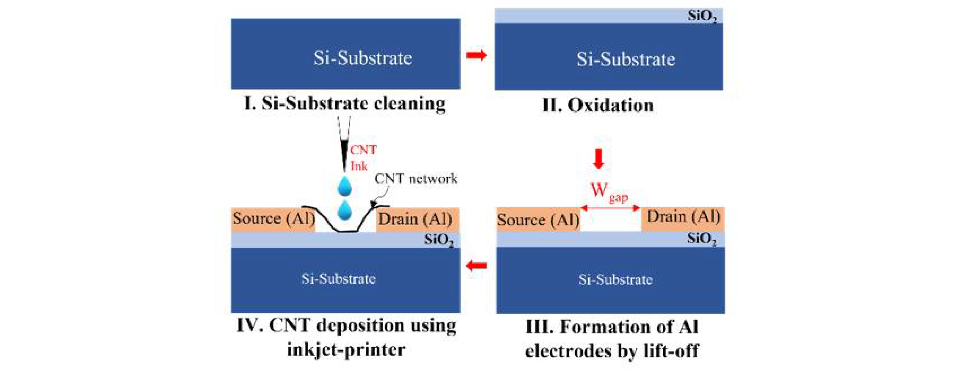
Abstract
:1. Introduction
2. Materials and Methods
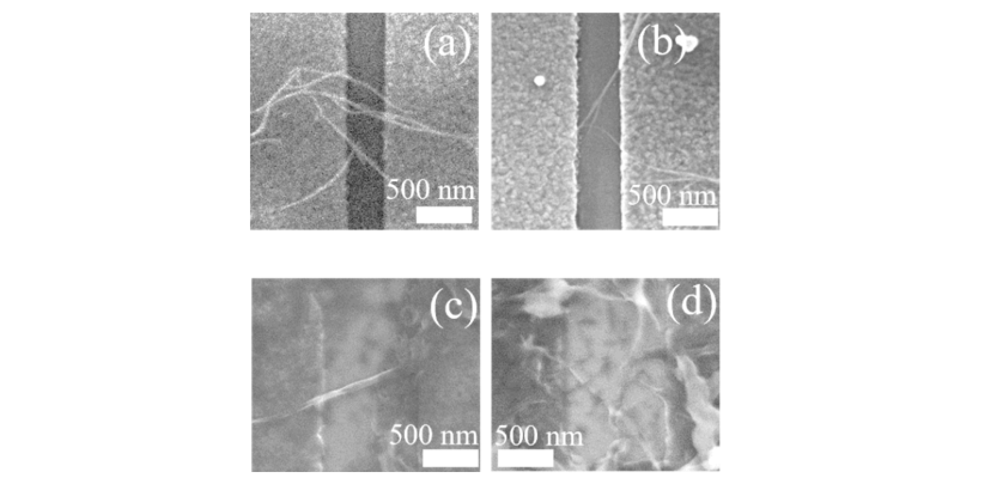
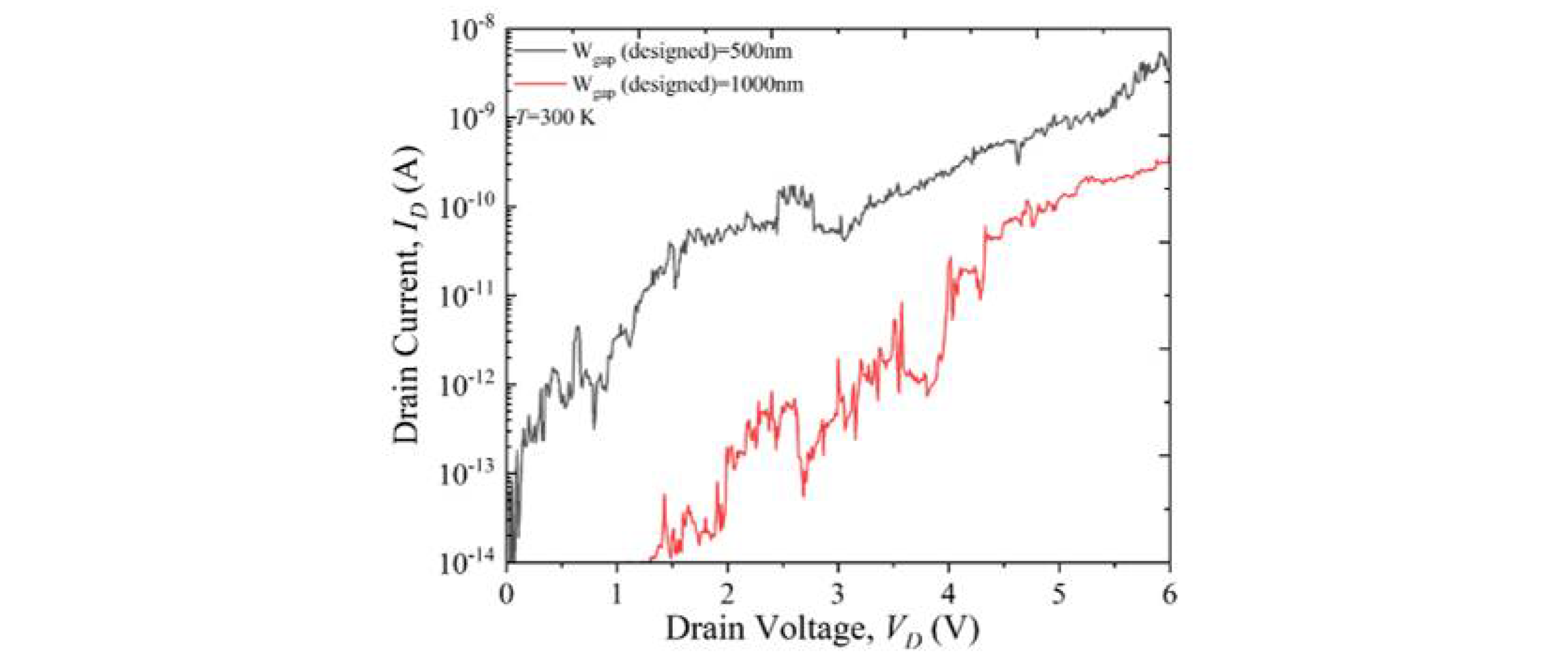
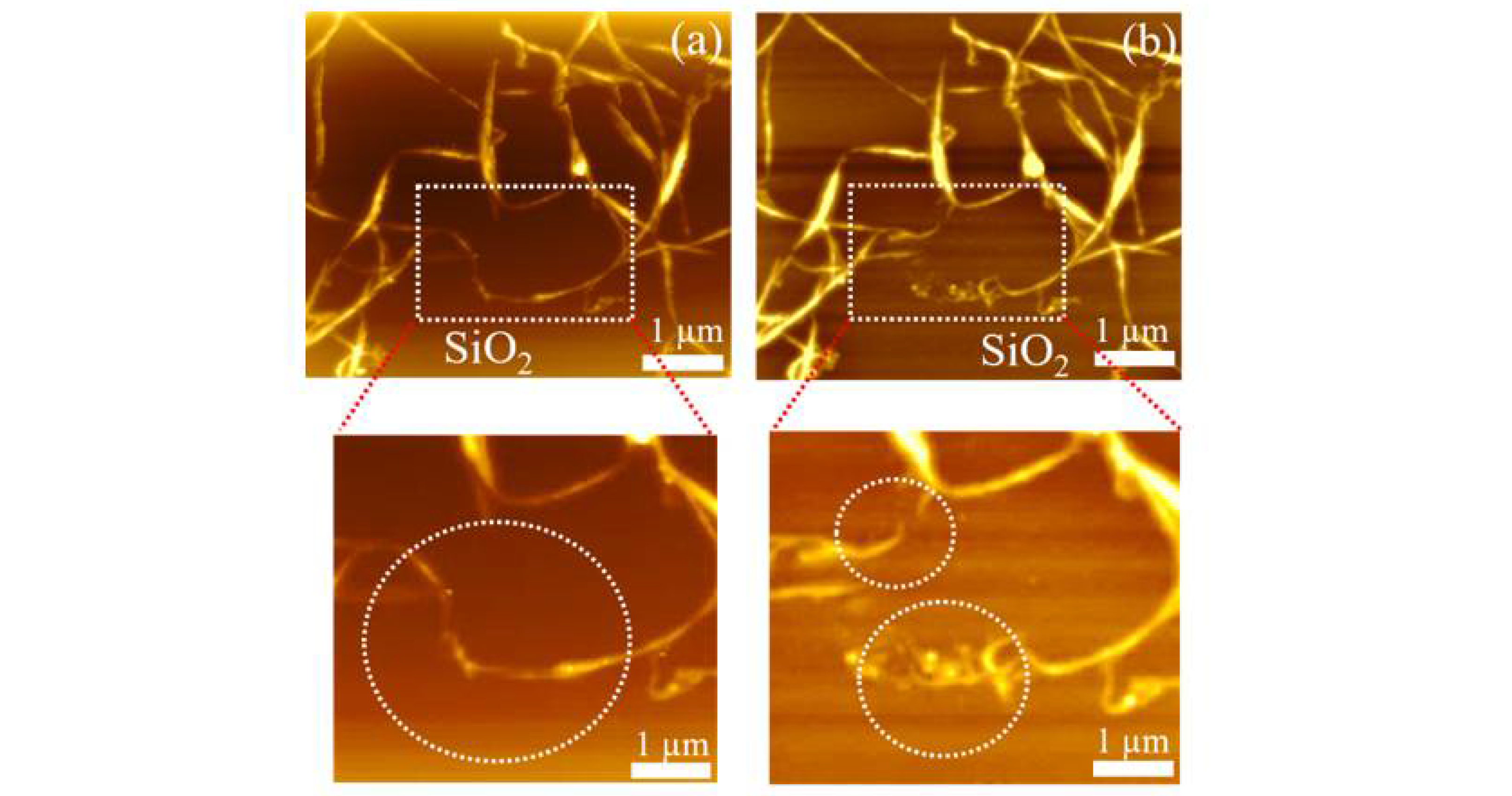
3. Results
4. Discussion
5. Conclusions
Supplementary Materials
Author Contributions
Funding
Institutional Review Board Statement
Informed Consent Statement
Data Availability Statement
Acknowledgments
Conflicts of Interest
References
- 2015 International Technology Roadmap for Semiconductors (ITRS 2015); Semiconductor Industry Association (SIA): Washington, DC, USA.
- Durkop, T.; Getty, S.A.; Cobas, E.; Fuhrer, M.S. Extraordinary Mobility in Semiconducting Carbon Nanotubes. Nano Lett. 2004, 4, 35–39. [Google Scholar] [CrossRef]
- Pop, E.; Mann, D.; Wang, Q.; Goodson, K.; Dai, H. Thermal conductance of an Individual Single-wall Carbon Nanotube above Room Temperature. Nano Lett. 2006, 6, 96–100. [Google Scholar] [CrossRef] [PubMed] [Green Version]
- Gspann, T.S.; Juckes, S.M.; Niven, J.F.; Johnson, M.B.; Elliott, J.A.; White, M.A.; Windle, A.H. High thermal conductivities of carbon nanotube films and micro-fibres and their dependence on morphology. Carbon 2017, 114, 160–168. [Google Scholar] [CrossRef] [Green Version]
- Snow, E.S.; Campbell, P.M.; Ancona, M.G.; Novak, J.P. High-mobility carbon-nanotube thin-film transistors on a polymeric substrate. Appl. Phys. Lett. 2005, 86, 033105. [Google Scholar] [CrossRef]
- Shahrjerdi, D.; Franklin, A.D.; Oida, S.; Ott, J.A.; Tulevski, G.S.; Haensch, W. High-performance Air-stable n-Type Carbon Nanotube transistors with Erbium Contacts. ACS Nano 2013, 7, 8303–8308. [Google Scholar] [CrossRef]
- Cai, L.; Song, L.; Luan, P.; Zhang, Q.; Zhang, N.; Gao, Q.; Zhao, D.; Zhang, X.; Tu, M.; Yang, F.; et al. Super-stretchable, Transparent Carbon Nanotube-based Capacitive Strain Sensors for Human Motion Detection. Sci. Rep. 2013, 3, 3048. [Google Scholar] [CrossRef] [Green Version]
- Cao, X.; Lau, C.; Liu, Y.; Wu, F.; Gui, H.; Liu, Q.; Ma, Y.; Wan, H.; Amer, M.R.; Zhou, C. Fully screen-printed, large-area, and flexible active-matrix electrochromic displays using carbon nanotube thin-film transistors. ACS Nano 2016, 10, 9816–9822. [Google Scholar] [CrossRef]
- Cai, L.; Zhang, S.; Miao, J.; Yu, Z.; Wang, C. Fully printed stretchable thin-film transistors and integrated logic circuits. ACS Nano 2016, 10, 11459–11468. [Google Scholar] [CrossRef]
- Lau, P.H.; Takei, K.; Wang, C.; Ju, Y.; Kim, J.; Yu, Z.; Takahashi, T.; Cho, G.; Javey, A. Fully printed high performance carbon nanotube thin-film transistors on flexible substrates. Nano Lett. 2013, 13, 3864. [Google Scholar] [CrossRef]
- Zhang, S.; Cai, L.; Wang, T.; Miao, J.; Sepulveda, N.; Wang, C. Fully printed carbon nanotube photodetectors. Appl. Phys. Lett. 2017, 110, 123105. [Google Scholar] [CrossRef] [Green Version]
- Yamada, T.; Hayamizu, Y.; Yamamoto, Y.; Yomogida, Y.; Izadi-Najafabadi, A.; Futaba, D.N.; Hata, K. A stretchable carbon nanotube strain sensor for human-motion detection. Nat. Nanotechnol. 2011, 6, 296–301. [Google Scholar] [CrossRef] [PubMed]
- Lee, D.; Seol, M.-L.; Moon, D.I.; Bennett, P.; Yoder, N.; Humes, J.; Bokor, J.; Choi, Y.-K.; Choi, S.-J. High-performance thin-film transistors produced from highly separated solution-processed carbon nanotubes. Appl. Phys. Lett. 2014, 104, 143508. [Google Scholar] [CrossRef] [Green Version]
- Choi, S.J.; Wang, C.; Lo, C.C.; Bennett, P.; Javey, A.; Bokor, J. Comparative study of solution-processed carbon nanotube network transistors. Appl. Phys. Lett. 2012, 101, 112104. [Google Scholar] [CrossRef] [Green Version]
- Choi, S.J.; Bennett, P.; Lee, D.; Bokor, J. Highly uniform carbon nanotube nanomesh network transistors. Nano Res. 2015, 8, 1320–1326. [Google Scholar] [CrossRef]
- Tortorich, R.P.; Choi, J.W. Inkjet printing of carbon nanotubes. Nanomaterials 2013, 3, 453–468. [Google Scholar] [CrossRef] [Green Version]
- Song, J.-W.; Kim, J.; Yoon, Y.H.; Choi, B.S.; Kim, J.H.; Han, C.S. Inkjet-printing of single-walled carbon nanotubes and electrical characterization of the line pattern. Nanotechnology 2008, 19, 095702. [Google Scholar] [CrossRef]
- Song, J.-W.; Kim, Y.-S.; Yoon, Y.-H.; Lee, E.S.; Han, C.S.; Cho, Y.; Kim, D.; Kim, J.; Lee, N.; Ko, Y.G.; et al. The production of transparent carbon nanotube field emitters using inkjet printing. Phys. E Low-Dimens. Syst. Nanostructures 2009, 41, 1513–1516. [Google Scholar] [CrossRef]
- Yang, L.; Zhang, R.; Staiculescu, D.; Wong, C.P.; Tentzeris, M.M. A novel conformal RFID-enabled module utilizing inkjet-printed antennas and carbon nanotubes for gas-detection applications. IEEE Antennas Wirel. Propag. Lett. 2009, 8, 653–656. [Google Scholar] [CrossRef] [Green Version]
- Yun, J.-H.; Chang-Soo, H.; Kim, J.; Song, J.-W.; Shin, D.-H.; Park, Y.G. Fabrication of carbon nanotube sensor device by inkjet printing. In Proceedings of the 3rd IEEE International Conference on Nano/Micro Engineered and Molecular Systems (NEMS), Sanya, China, 6–9 January 2008. [Google Scholar]
- Fan, Z.; Wei, T.; Luo, G.; Wei, F. Fabrication and characterization of multi-walled carbon nanotubes-based ink. J. Mater. Sci. 2005, 40, 5075–5077. [Google Scholar] [CrossRef]
- Matsuzaki, S.; Nobusa, Y.; Shimizu, R.; Yanagi, K.; Kataura, H.; Takenobu, T. Continuous electron doping of single-walled carbon nanotube films using inkjet technique. Jpn. J. Appl. Phys. 2012, 51, 06FD18. [Google Scholar] [CrossRef]
- Okimoto, H.; Takenobu, T.; Yanagi, K.; Miyata, Y.; Shimotani, H.; Kataura, H.; Iwasa, Y. Tunable carbon nanotube thin-film transistors produced exclusively via inkjet printing. Adv. Mater. 2010, 22, 3981–3986. [Google Scholar] [CrossRef] [PubMed]
- Beecher, P.; Servati, P.; Rozhin, A.; Colli, A.; Scardaci, V.; Pisana, S.; Hasan, T.; Flewitt, A.J.; Robertson, J.; Hsieh, G.W.; et al. Ink-jet printing of carbon nanotube thin film transistors. J. Appl. Phys. 2007, 102, 043710. [Google Scholar] [CrossRef] [Green Version]
- Kordás, K.; Mustonen, T.; Tóth, G.; Jantunen, H.; Lajunen, M.; Soldano, C.; Talapatra, S.; Kar, S.; Vajtai, R.; Ajayan, P.M. Inkjet printing of electrically conductive patterns of carbon nanotubes. Small 2006, 2, 1021–1025. [Google Scholar] [CrossRef] [PubMed]
- Mustonen, T.; Maklin, J.; Kordás, K.; Halonen, N.; Tóth, G.; Saukko, S.; Vähäkangas, J.; Jantunen, H.; Kar, S.; Ajayan, P.M.; et al. Controlled ohmic and nonlinear electrical transport in inkjet-printed single-wall carbon nanotube films. Phys. Rev. B Cond. Matter and Mater. Phys. 2008, 77, 125430. [Google Scholar] [CrossRef]
- Garcia-Espino, E.; Sala, G.; Pino, F.; Halonen, N.; Luomahaara, J.; Mäklin, J.; Tóth, G.; Kordás, K.; Jantunen, H.; Terrones, M.; et al. Electrical transport and field-effect transistors using inkjet-printed SWCNT films having different functional side groups. ACS Nano 2010, 4, 3318–3324. [Google Scholar] [CrossRef]
- Llinas, J.P.; Hekmaty, M.A.; Talin, A.; Leonard, F. Origami terahertz detectors realized by inkjet printing of carbon nanotube inks. ACS Appl. Nano. Mater. 2020, 3, 2920–2927. [Google Scholar] [CrossRef]
- Ervasti, H.; Jarvinen, T.; Pitkanen, O.; Bozo, E.; Hiitola-Keinanen, J.; Huttunen, O.; Hiltunen, J.; Kordas, K. Inkjet-deposited single-wall carbon nanotube micropatterns on stretchable PDMS-Ag substrate-electrode structures for piezoresistive strain sensing. ACS Appl. Mater. Interfaces 2021, 13, 27284–27294. [Google Scholar] [CrossRef]
- O’Connell, M.J.; Bachilo, S.M.; Huffman, C.B.; Moore, V.C.; Strano, M.S.; Haroz, E.H.; Rialon, K.L.; Boul, P.J.; Noon, W.H.; Kittrell, C.; et al. Band gap fluorescence from individual single-walled carbon nanotubes. Science 2002, 297, 593–596. [Google Scholar] [CrossRef] [Green Version]
- Lu, K.L.; Lago, R.M.; Chen, Y.K.; Green, M.L.H.; Harris, P.J.F.; Tsang, S.C. Mechanical damage of carbon nanotube by ultrasound. Carbon 1996, 34, 814–816. [Google Scholar] [CrossRef]
- Rennhofer, H.; Zanghellini, B. Dispersion state and damage of carbon nanotubes and carbon nanofibers by ultrasonic dispersion: A Review. Nanomaterials 2021, 11, 1469. [Google Scholar] [CrossRef]
- Lin, Y.-M.; Appenzeller, J.; Avouris, P. Ambipolar-to-unipolar conversion of carbon nanotube transistors by gate structure engineering. Nano Lett. 2004, 4, 947–950. [Google Scholar] [CrossRef] [Green Version]
- Iwata, F.; Ohashi, Y.; Ishisaki, I.; Picco, L.M.; Ushiki, T. Development of nanomanipulator using a high-speed atomic force microscope coupled with a haptic device. Ultramicroscopy 2013, 133, 88–94. [Google Scholar] [CrossRef] [PubMed]
- Kashiwase, Y.; Ikeda, T.; Oya, T.; Ogino, T. Manipulation and soldering of carbon nanotubes using atomic force microscope. Appl. Surf. Sci. 2008, 254, 7897–7900. [Google Scholar] [CrossRef]
- Kumar, S.; Kaur, I.; Kumari, N.; Jain, S.; Dharamveer, K.; Jindal, V.K.; Verma, N.K.; Bharadwaj, L.M. Atomic force microscope manipulation of multiwalled and single walled carbon nanotubes with reflux and ultrasonic treatments. Appl. Nanosci. 2014, 4, 19–26. [Google Scholar] [CrossRef] [Green Version]


Publisher’s Note: MDPI stays neutral with regard to jurisdictional claims in published maps and institutional affiliations. |
© 2022 by the authors. Licensee MDPI, Basel, Switzerland. This article is an open access article distributed under the terms and conditions of the Creative Commons Attribution (CC BY) license (https://creativecommons.org/licenses/by/4.0/).
Share and Cite
Singh, R.S.; Takagi, K.; Aoki, T.; Moon, J.H.; Neo, Y.; Iwata, F.; Mimura, H.; Moraru, D. Precise Deposition of Carbon Nanotube Bundles by Inkjet-Printing on a CMOS-Compatible Platform. Materials 2022, 15, 4935. https://doi.org/10.3390/ma15144935
Singh RS, Takagi K, Aoki T, Moon JH, Neo Y, Iwata F, Mimura H, Moraru D. Precise Deposition of Carbon Nanotube Bundles by Inkjet-Printing on a CMOS-Compatible Platform. Materials. 2022; 15(14):4935. https://doi.org/10.3390/ma15144935
Chicago/Turabian StyleSingh, Rohitkumar Shailendra, Katsuyuki Takagi, Toru Aoki, Jong Hyun Moon, Yoichiro Neo, Futoshi Iwata, Hidenori Mimura, and Daniel Moraru. 2022. "Precise Deposition of Carbon Nanotube Bundles by Inkjet-Printing on a CMOS-Compatible Platform" Materials 15, no. 14: 4935. https://doi.org/10.3390/ma15144935