
Development of Wide-Angle Short-Wave Pass Thin Film Based on the Ultra-Thin Silicate Glass


Abstract
:1. Introduction
1.1. Laser Chemical
1.2. Cathode Sputtering
1.3. Silica Thin Film
2. Experiment
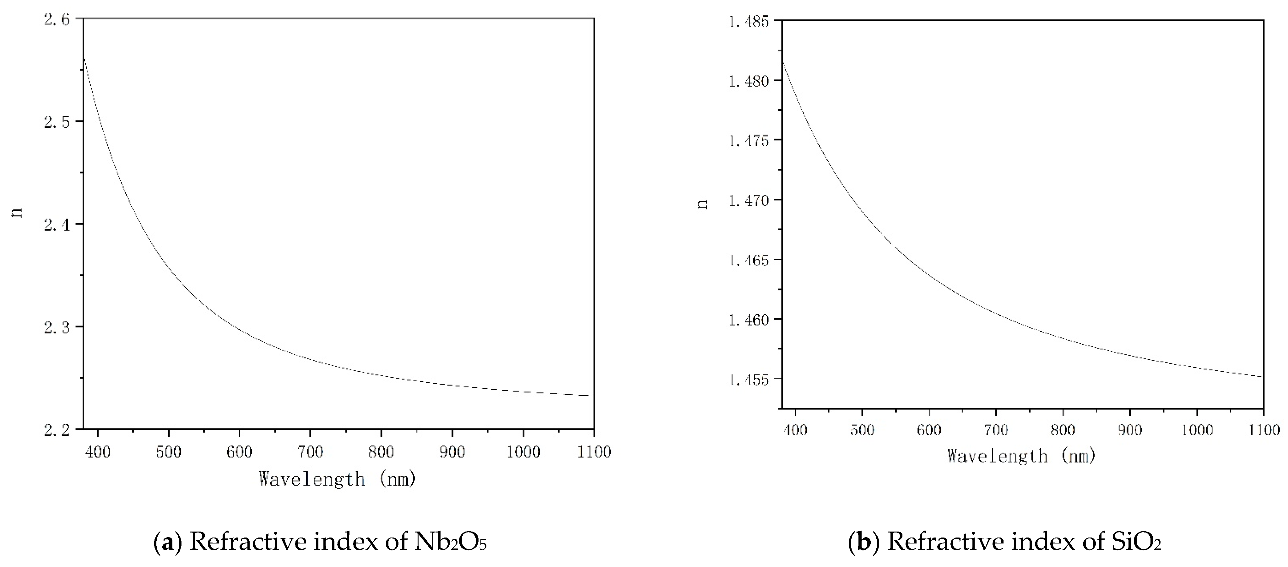
2.1. Material
2.2. Film Stack Design
2.3. Preparation Methods
3. Testing and Analysis
3.1. Firmness Tests and Analysis
3.2. Firmness Tests and Stress Tests
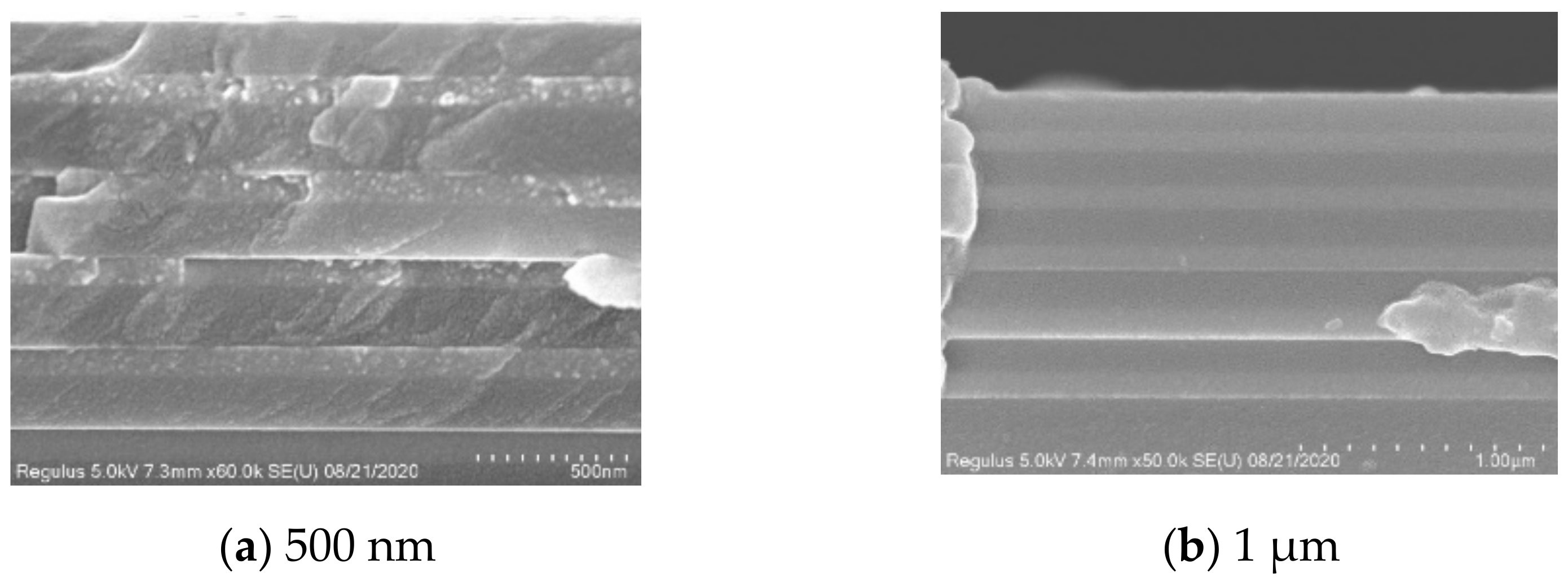
3.3. Scanning Electron Microscope Tests and Analysis
3.4. Spectral Test
4. Results and Discussion
5. Conclusions
Author Contributions
Funding
Institutional Review Board Statement
Informed Consent Statement
Data Availability Statement
Conflicts of Interest
References
- Li, W.Q.; Mu, C.Y. Charging effects of SiO2 thin film on Si substrate irradiated by penetrating electron beam. Micron 2021, 140, 102961. [Google Scholar] [CrossRef] [PubMed]
- Yu, L.F.; Ye, Y.T.; Wu, J.P. Defect detection and control of a laser conditioning system for large diameter optical film. Laser Technol. 2012, 36, 188–190. [Google Scholar]
- Amato, A.; Cagnoli, G.; Granata, M.; Sassolas, B.; Degallaix, J.; Forest, D.; Michel, C.; Pinard, L.; Demos, N.; Gras, S.; et al. Optical and mechanical properties of ion-beam-sputtered Nb2O5 and TiO2-Nb2O5 thin films for gravitational-wave interferometers and an improved measurement of coating thermal noise in Advanced LIGO. Phys. Rev. D 2021, 103, 072001. [Google Scholar] [CrossRef]
- Zhang, Y.; Zhang, Y.; Ling, N.; Xu, H. Research on Finite Element Analysis of Thin Film Residual Stress. Prog. Laser Optoelectron. 2005, 42, 5. [Google Scholar]
- Zhang, B.; Chen, T.; Xiong, Y.; Wang, D.; Wang, C. Research on the design and plating technology of mid-wave infrared short-wave pass filter. Vac. Cryog. 2010, 3, 148–152. [Google Scholar]
- Zhao, X.; Shi, J.; Guo, H. Short-wave pass filter film system design. Appl. Opt. 2006, 5, 415–418. [Google Scholar]
- Leng, J.; Xue, W.; Yu, Z.; Lu, W.; Wang, H.; Zhang, D. On-line measurement and research of TiO2 and SiO2 film stress. J. Vac. Sci. Technol. 2011, 31, 465–469. [Google Scholar]
- Rani, R.A.; Zoolfakar, A.S.; O’Mullane, A.P.; Austin, M.W.; Kalantar-zadeh, K. Thin films and nanostructures of niobium pentoxide: Fundamental properties, synthesis methods and applications. J. Mater. Chem. A 2014, 2, 15683–15703. [Google Scholar] [CrossRef] [Green Version]
- Hoffmann, M.R.; Martin, S.T.; Choi, W.; Bahnemann, D.W. Environmental application of semiconductor photocatalysis. Chem. Rev. 1995, 95, 69–96. [Google Scholar] [CrossRef]
- Wang, X.; Fang, W.; Liu, F. Material properties of MoOx thin film prepared by magnetron sputtering. Acta Sol. Energy 2020, 3, 212–218. [Google Scholar]
- Stoney, G.G. The tension of metallic films deposited by electrol-ysis. Soc. Lond. Ser. A 1909, 82, 172–175. [Google Scholar]
- Maschietto, M.; Dal Maschio, M.; Girardi, S.; Vassanelli, S. In situ electroporation of mammalian cells through SiO2 thin film capacitive microelectrodes. Sci. Rep. 2021, 11, 15126. [Google Scholar] [CrossRef] [PubMed]
- Park, C.; Lee, J.; Kwon, K.S.; Cho, K.Y.; Kim, J. Fabrication of electrochromic devices by laser patterning of spin-sprayed transparent conductive Ga: ZnO films. Ceram. Int. 2021, 47, 6470–6478. [Google Scholar] [CrossRef]
- Zhang, L.; Xiao, X.; Qi, H.; Huang, Y.; Qin, H. Quantitative and nondestructive determination of residual stress for SiO2 thin film by laser-generated surface acoustic wave technique. Meas. Sci. Technol. 2022, 33, 045601. [Google Scholar] [CrossRef]
- Harashima, T.; Kinoshita, J.I.; Kimura, Y.; Brugnera, A., Jr.; Zanin, F.; Pecora, J.D.; Matsumoto, K. Morphological comparative study on ablation of dental hard tissue at cavity preparation by Er: YAG and Er, CR: YSGG lasers. Photomed. Laser Surg. 2005, 23, 52–55. [Google Scholar] [CrossRef]
- Ishikawa, I.; Aoki, A.; Takasaki, A.A. Clinical application of erbium: YAG Laser in periodontology. J. Int. Acad. Periodontol. 2008, 10, 22–30. [Google Scholar]
- Teer, G. Technical note: A magnetron sputter ion-plating system. Surf. Coat. Technol. 1989, 39, 565. [Google Scholar] [CrossRef]
- Sproul, W.D.; Rudnik, P.J.; Graham, M.E.; Rohde, S.L. High rate reactive sputtering in an opposed cathode closed-field unbalanced magnetron sputtering system. Surf. Coat. Technol. 1990, 43, 270–278. [Google Scholar] [CrossRef]
- Sulieman, M. An overview of the use of lasers in general dentist practice: Laser physics and tissue interactions. Dent. Update 2005, 32, 228–236. [Google Scholar] [CrossRef]
- Bhattarai, M.K.; Mishra, K.K.; Instan, A.A.; Bastakoti, B.P.; Katiyar, R.S. Enhanced energy storage density in Sc3+ substituted Pb(Zr0.53Ti0.47)O3 nanoscale films by pulse laser deposition technique. Appl. Surf. Sci. 2019, 490, 451. [Google Scholar] [CrossRef]
- McNerny, D.Q.; Viswanath, B.; Copic, D.; Laye, F.R.; Prohoda, C.; Brieland-Shoultz, A.C.; Polsen, E.S.; Dee, N.T.; Veerasamy, V.S.; Hart, A.J. Direct fabrication of graphene on SiO2 enabled by thin film stress engineering. Sci. Rep. 2014, 4, 5049. [Google Scholar] [CrossRef] [PubMed] [Green Version]
- Weiner, G.P. Laser dentistry practice management. Dent. Clin. N. Am. 2004, 48, 1105–1126. [Google Scholar] [CrossRef] [PubMed]
- Lee, B.J.; Seo, D.W.; Choi, J.W. Analysis of the influence of disk and wafer rotation speed on the SiO2 thin-film characteristics in a space-divided PE-ALD system. J. Korean Phys. Soc. 2021, 79, 638–647. [Google Scholar] [CrossRef]
- Loevschall, H.; Arenholtd-Bindslev, D. Effect of low level diode laser irradiation of human oral mucosa fibroblasts in vitro. Lasers Surg. Med. 1994, 14, 347–354. [Google Scholar] [CrossRef] [PubMed]
- Noble, P.B.; Shields, E.D.; Blecher, P.D.; Bentley, K.C. Locomotory characteristics of fibroblasts within a three-dimensional collagenlattice: Modulation by a helium/neon soft laser. Lasers Surg. Med. 1992, 12, 669–674. [Google Scholar] [CrossRef]
- Asencio Arana, F.; Garcia, F.V.; Molina Andreu, E.; Vidal, M.J.; Martinez, S.F. Endoscopic enhancement of the healing of high risk colon anastomoses by low-power helium-neon laser. An experimental study. Dis. Colon Rectum. 1992, 35, 568–573. [Google Scholar] [CrossRef]
- Pourreau-Schneider, N.; Ahmed, A.; Soudry, M.; Jacquemier, J.; Kopp, F.; Franquin, J.C.; Martin, P. Helium-neon laser treatment transforms fibroblasts into myofibroblasts. Am. J. Pathol. 1990, 137, 171–178. [Google Scholar]
- Neiburger, E.J. The effect of low-power lasers on intraoral wound healing. N. Y. State Dent. J. 1995, 61, 40–43. [Google Scholar]
- Kurumada, F. A study on the application of Ga-As semiconductor laser to endodontics. The effects of laser irradiation on the activation of inflammatory cells and the vital pulpotomy. Ohu Daigaku Shigakushi 1990, 17, 233–244. [Google Scholar]
- Kitsmaniuk, Z.D.; Demochko, V.B.; Popovich, V.I. The use of low energy lasers for preventing and treating postoperative and radiation-induced complications in patients with head and neck tumors. Vopr. Onkol. 1992, 38, 980–986. [Google Scholar]
- Lira-Cantu, M.; Krebs, F.C. Hybrid solar cells based on MEH-PPV and thin film semiconductor oxides (TiO2, Nb2O5, ZnO, CeO2 and CeO2–TiO2): Performance improvement during long-time irradiation. Sol. Energy Mater. Sol. Cells 2006, 90, 2076–2086. [Google Scholar] [CrossRef]
- Pond, B.J.; DeBar, J.I.; Carniglia, C.K.; Raj, T. Stress reduction in ion beam sputtered mixed oxide films. Appl. Opt. 1989, 28, 2800–2805. [Google Scholar] [CrossRef] [PubMed]
- Windischmann, H. Intrinsic stress in sputtered thin films. J. Vac. Sci. 1991, A9, 2431–2436. [Google Scholar] [CrossRef]
- Shao, S. Study of the Origin Mechanism and Controlling Method of Stress in Thin Films. Ph.D. Thesis, Shanghai Institute of Optics and Fine Mechanic, Shanghai, China, 2002; pp. 18–20. [Google Scholar]
- Martin, P.J.; Netterfield, R.P.; Sainty, W.G. Modification of the optical and structural properties of dielectric ZrO2 films by ion-assisted deposition. J. Appl. Phys. 1984, 55, 235–241. [Google Scholar] [CrossRef]
- Qin, Y.W. Film thickness measurement based on optical coherence tomography. Laser Technol. 2012, 36, 662–664. [Google Scholar]
- Tokas, R.B.; Sahoo, N.K.; Thakur, S.; Kamble, N.M. A comparative morphological study of electron beam co-deposited binary optical thin films of HfO2: SiO2 and ZrO2: SiO2. Curr. Appl. Phys. 2007, 8, 589–602. [Google Scholar] [CrossRef]
- Ren, H.; Zeng, Q.; Liang, X.H. Characteristics of Nd: Y3Al5O12 thin film prepared by electron beam evaporation deposition. Laser Technol. 2012, 36, 450–452. [Google Scholar]
- Schell-Sorokin, A.J.; Tromp, R.M. Mechanical stresses in (sub) monolayer epitaxial films. Phys. Rev. Lett. 1990, 64, 1039–1042. [Google Scholar] [CrossRef]
- Thornton, J.A.; Hoffman, D.W. Stress-related effects in thin films. Thin Solid Film. 1989, 171, 5–31. [Google Scholar] [CrossRef]
- Reicherd, W.; Mcco, R.; Mack, S.A. Production of thin film optical coatings with predetermined stress levels. In Imaging Technology and Telescopes; SPIE: Bellingham, WA, USA, 2000; Volume 4091, pp. 104–110. [Google Scholar]
- Ghang, Y.; Jin, C.; Li, C.; Deng, W.; Jin, J. ArF excimer laser induced damage on high reflective fluoride films. Laser Technol. 2014, 38, 302–306. [Google Scholar]


| Incident Angle/° | Wavelength/nm | Transmittance/% |
|---|---|---|
| 0 | 410~810 | >96 |
| 850~1100 | <1 | |
| 35 | 410~775 | >96 |
| 830~1100 | <1 |
| Num | Thickness | Num | Thickness | Num | Thickness | Num | Thickness | Num | Thickness |
|---|---|---|---|---|---|---|---|---|---|
| Sub | 15 | 0.58L | 30 | 0.37H | 45 | 0.38L | 60 | 2.10H | |
| 1 | 0.48L | 16 | 2.11H | 31 | 0.48L | 46 | 0.44H | 61 | 0.36L |
| 2 | 0.51H | 17 | 2.09L | 32 | 2.03H | 47 | 0.39L | 62 | 0.44H |
| 3 | 0.26L | 18 | 1.94H | 33 | 0.46L | 48 | 2.14H | 63 | 0.40L |
| 4 | 1.11H | 19 | 2.03L | 34 | 0.39H | 49 | 0.36L | 64 | 2.16H |
| 5 | 0.21L | 20 | 1.87H | 35 | 0.44L | 50 | 0.46H | 65 | 0.51L |
| 6 | 0.55H | 21 | 0.59L | 36 | 2.03H | 51 | 0.34L | 66 | 0.33H |
| 7 | 2.16L | 22 | 0.26H | 37 | 0.40L | 52 | 2.10H | 67 | 0.53L |
| 8 | 1.96H | 23 | 0.60L | 38 | 0.39H | 53 | 0.31L | 68 | 2.08H |
| 9 | 2.05L | 24 | 1.98H | 39 | 0.42L | 54 | 0.50H | 69 | 0.46L |
| 10 | 1.92H | 25 | 0.57L | 40 | 2.11H | 55 | 0.34L | 70 | 0.37H |
| 11 | 2.04L | 26 | 0.29H | 41 | 0.43L | 56 | 2.12H | 71 | 0.45L |
| 12 | 2.05H | 27 | 0.59L | 42 | 0.41H | 57 | 0.39L | 72 | 1.89H |
| 13 | 0.62L | 28 | 2.01H | 43 | 0.43L | 58 | 0.43H | 73 | 0.87L |
| 14 | 0.34H | 29 | 0.47L | 44 | 2.10H | 59 | 0.35L | Air |
Publisher’s Note: MDPI stays neutral with regard to jurisdictional claims in published maps and institutional affiliations. |
© 2022 by the authors. Licensee MDPI, Basel, Switzerland. This article is an open access article distributed under the terms and conditions of the Creative Commons Attribution (CC BY) license (https://creativecommons.org/licenses/by/4.0/).
Share and Cite
Fu, X.; Dong, S.; Xiong, S.; Li, C.; Chen, X. Development of Wide-Angle Short-Wave Pass Thin Film Based on the Ultra-Thin Silicate Glass. Materials 2022, 15, 4706. https://doi.org/10.3390/ma15134706
Fu X, Dong S, Xiong S, Li C, Chen X. Development of Wide-Angle Short-Wave Pass Thin Film Based on the Ultra-Thin Silicate Glass. Materials. 2022; 15(13):4706. https://doi.org/10.3390/ma15134706
Chicago/Turabian StyleFu, Xiuhua, Suotao Dong, Shifu Xiong, Cheng Li, and Xiaodong Chen. 2022. "Development of Wide-Angle Short-Wave Pass Thin Film Based on the Ultra-Thin Silicate Glass" Materials 15, no. 13: 4706. https://doi.org/10.3390/ma15134706