
Polarization Independent Metamaterial Absorber with Anti-Reflection Coating Nanoarchitectonics for Visible and Infrared Window Applications

 , , , , ,
Abstract
:1. Introduction
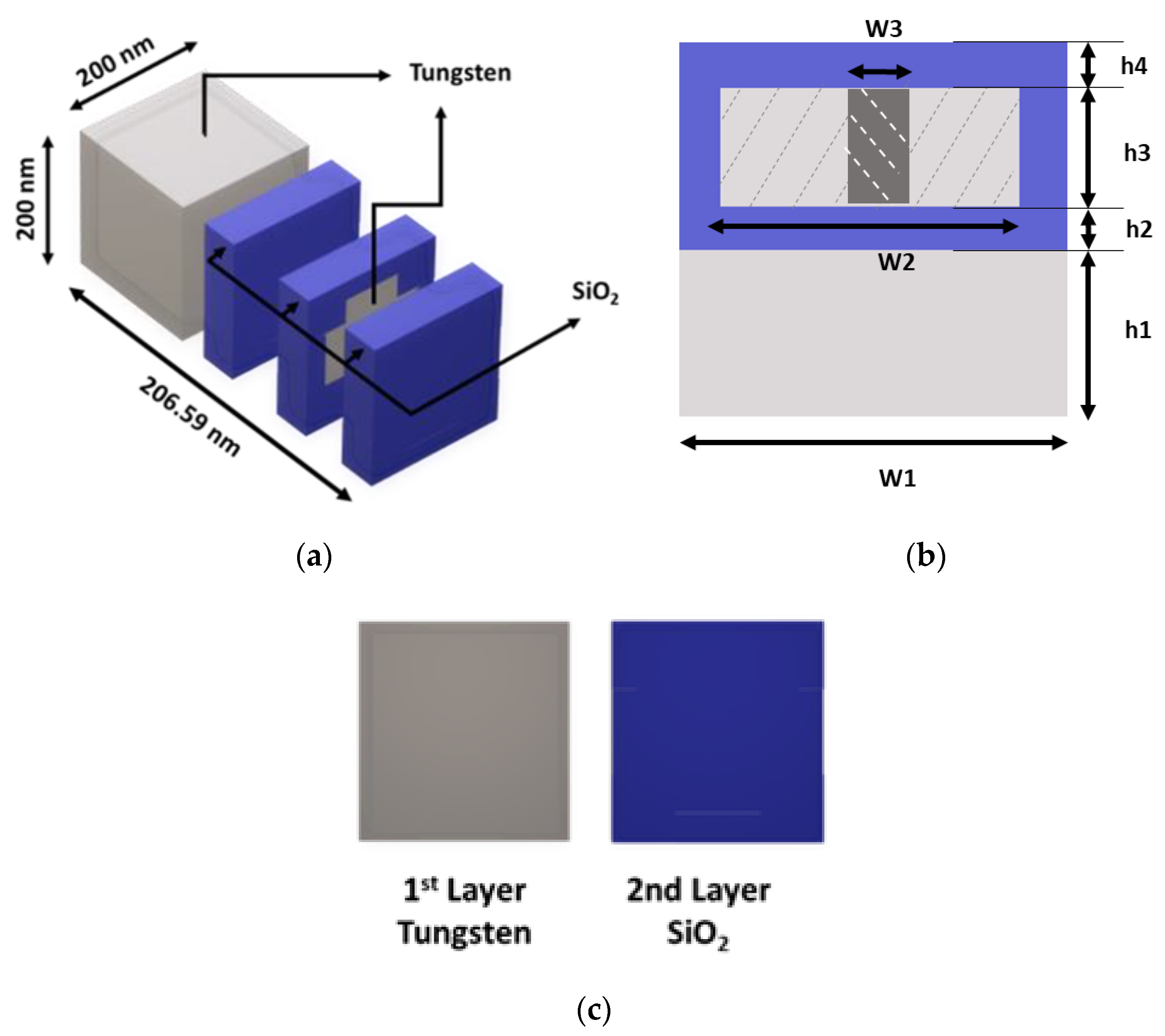
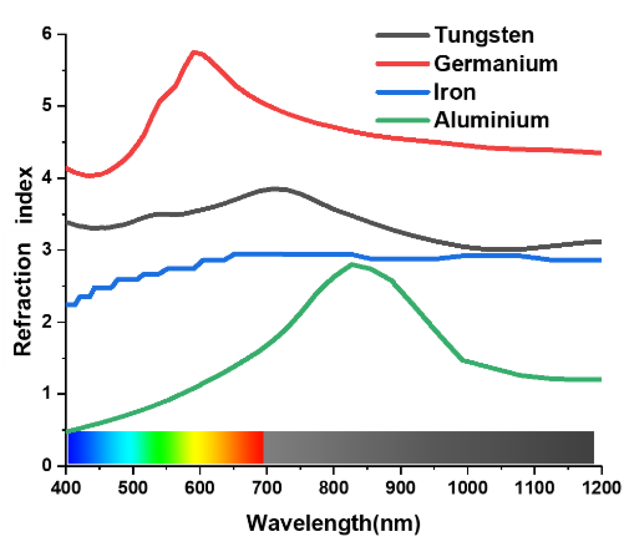
2. Unit Cell Design
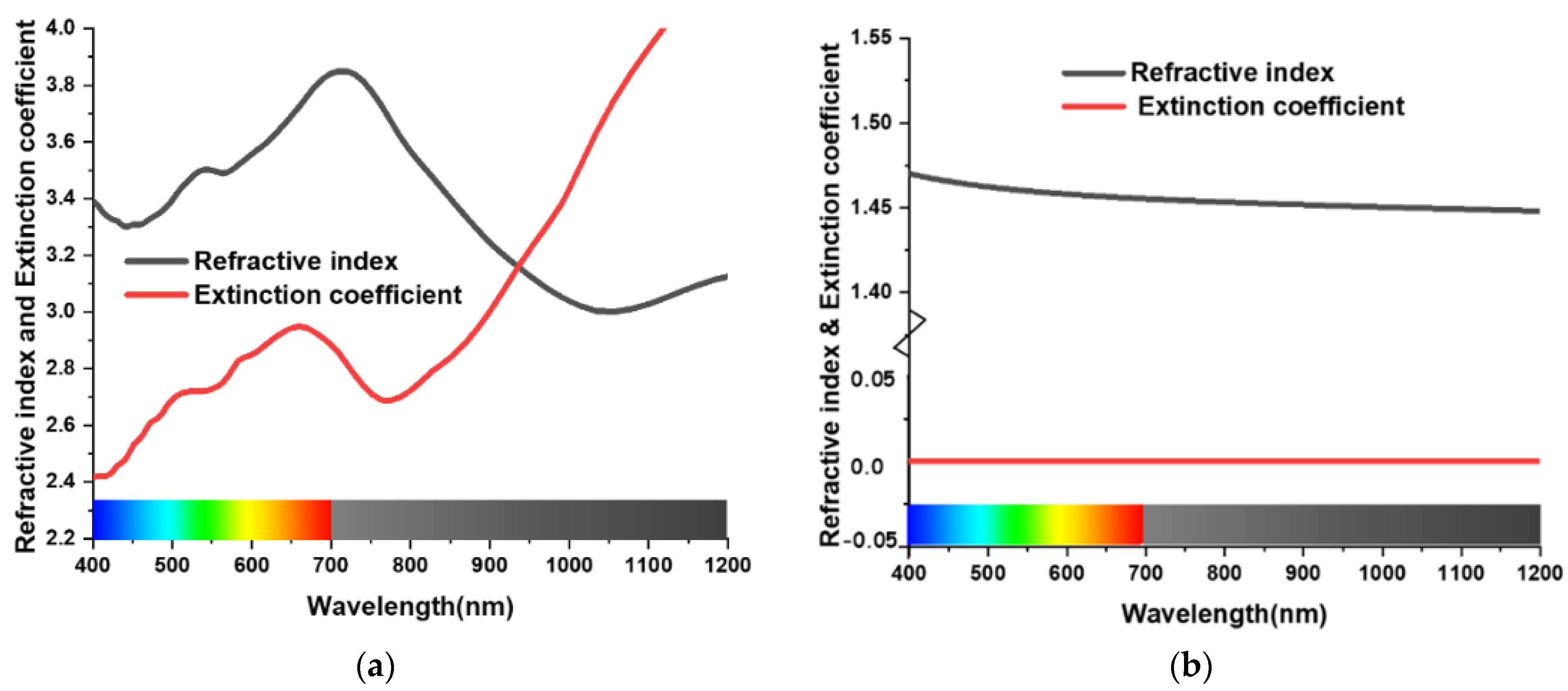
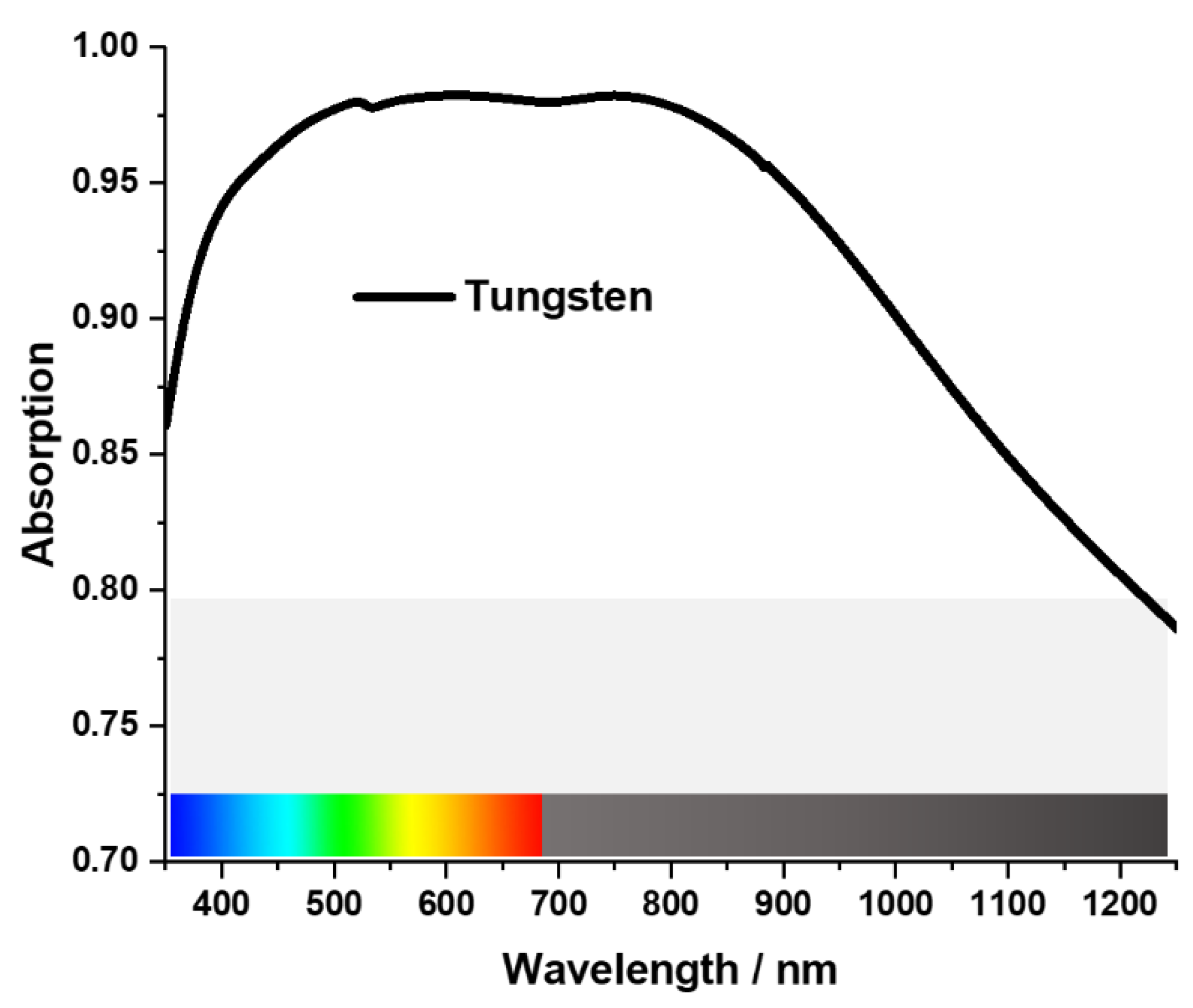
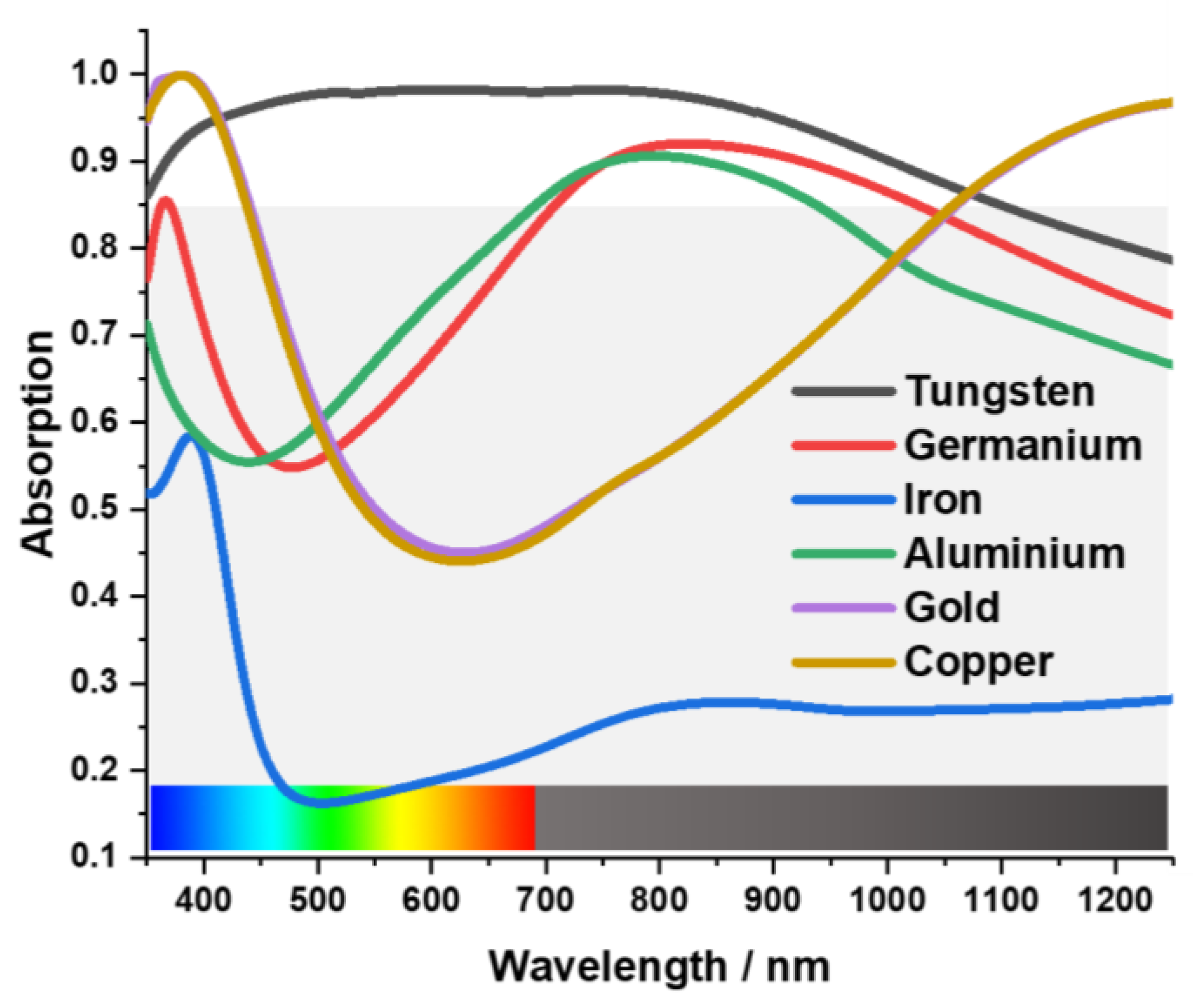
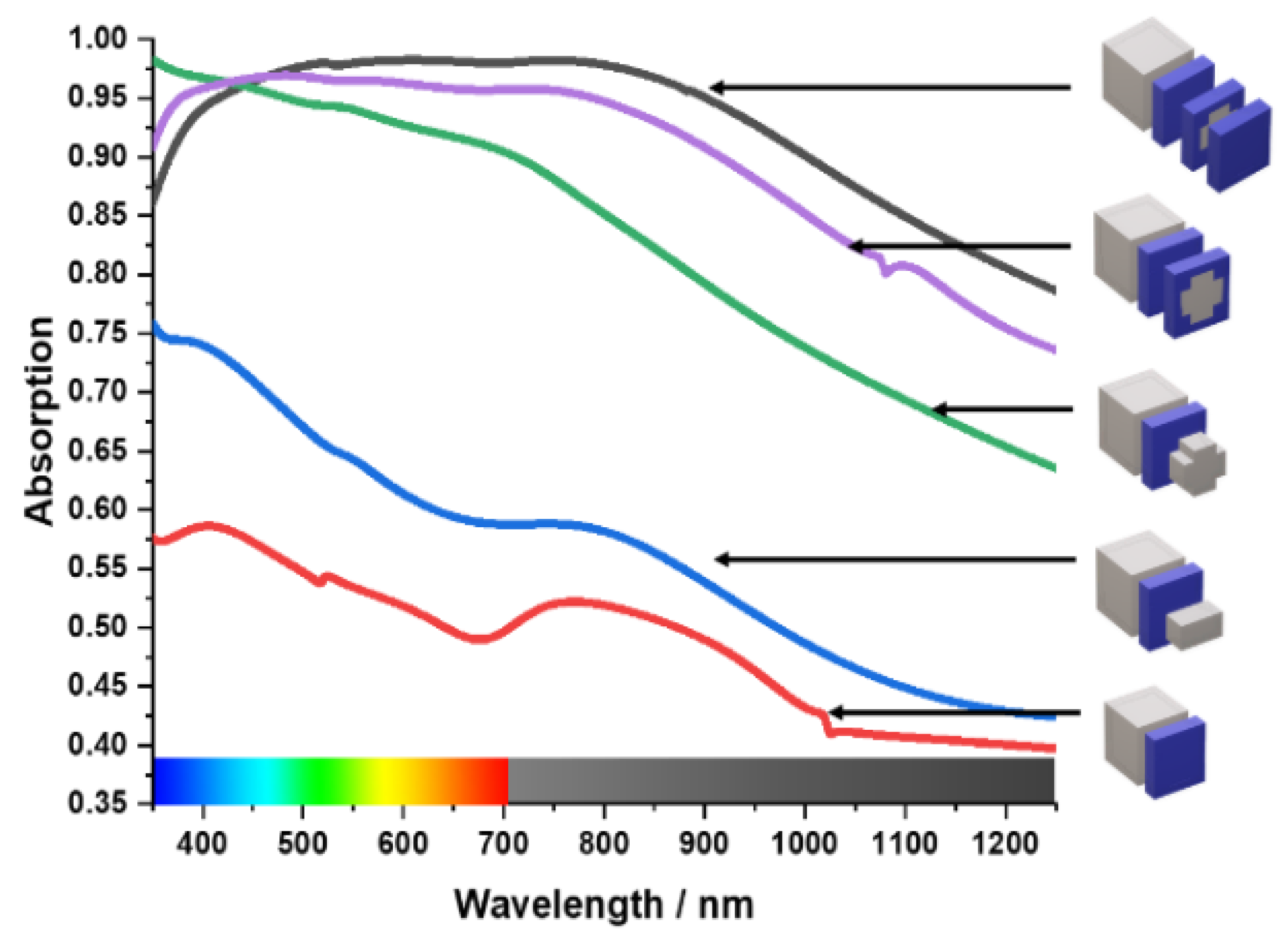
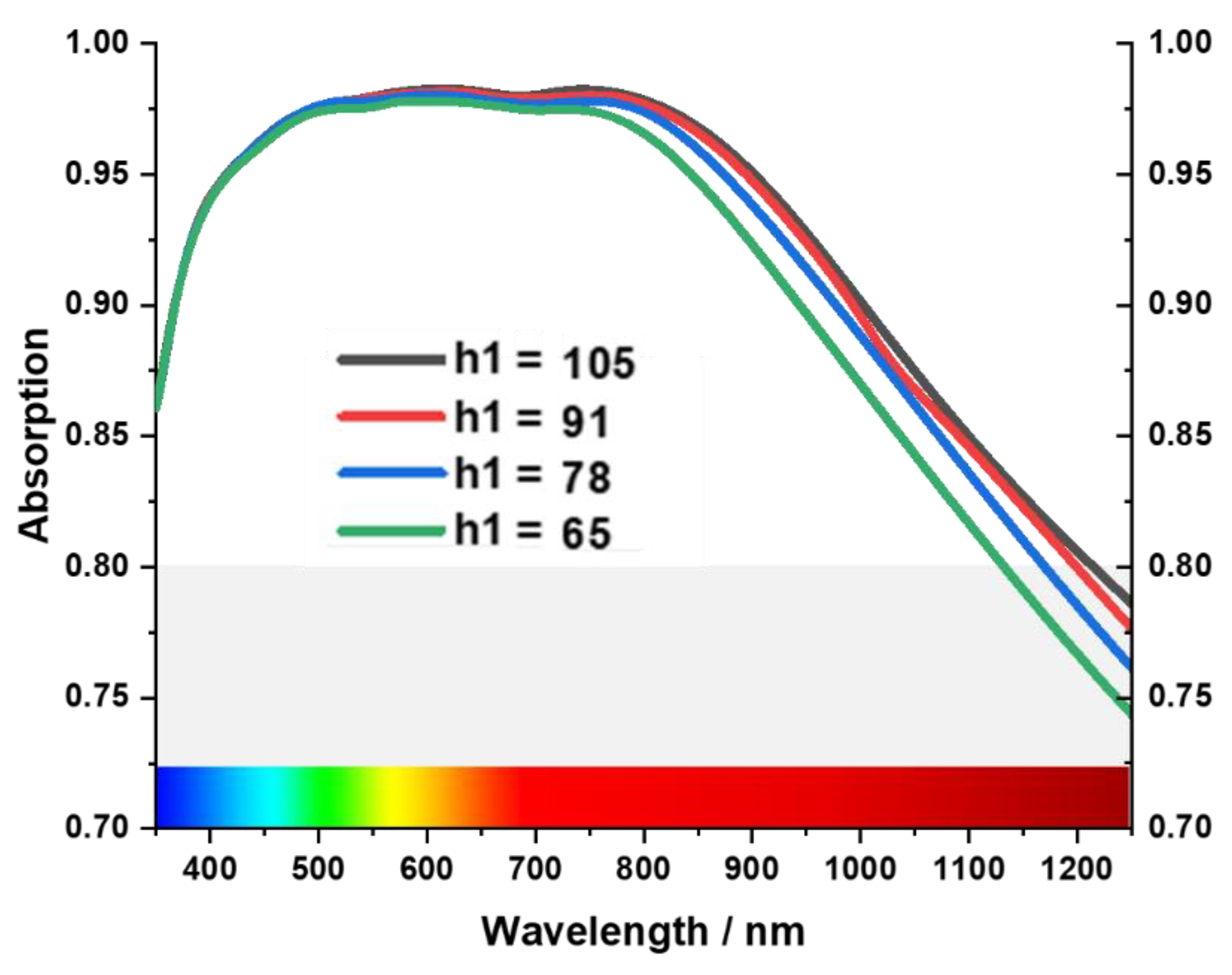
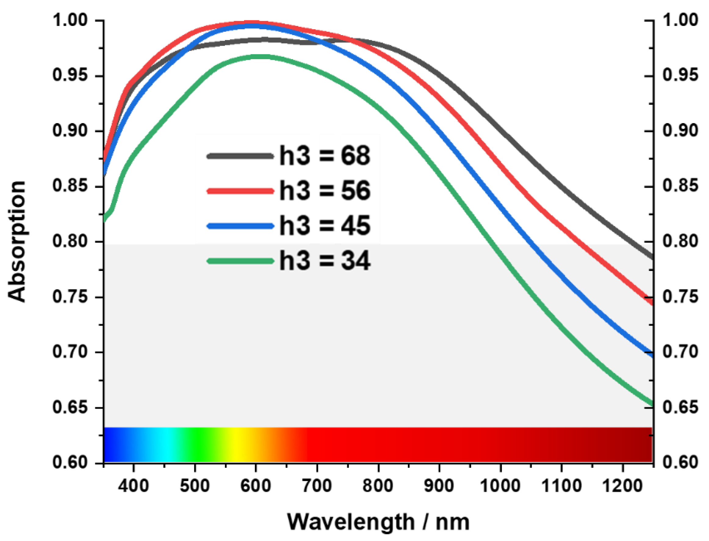
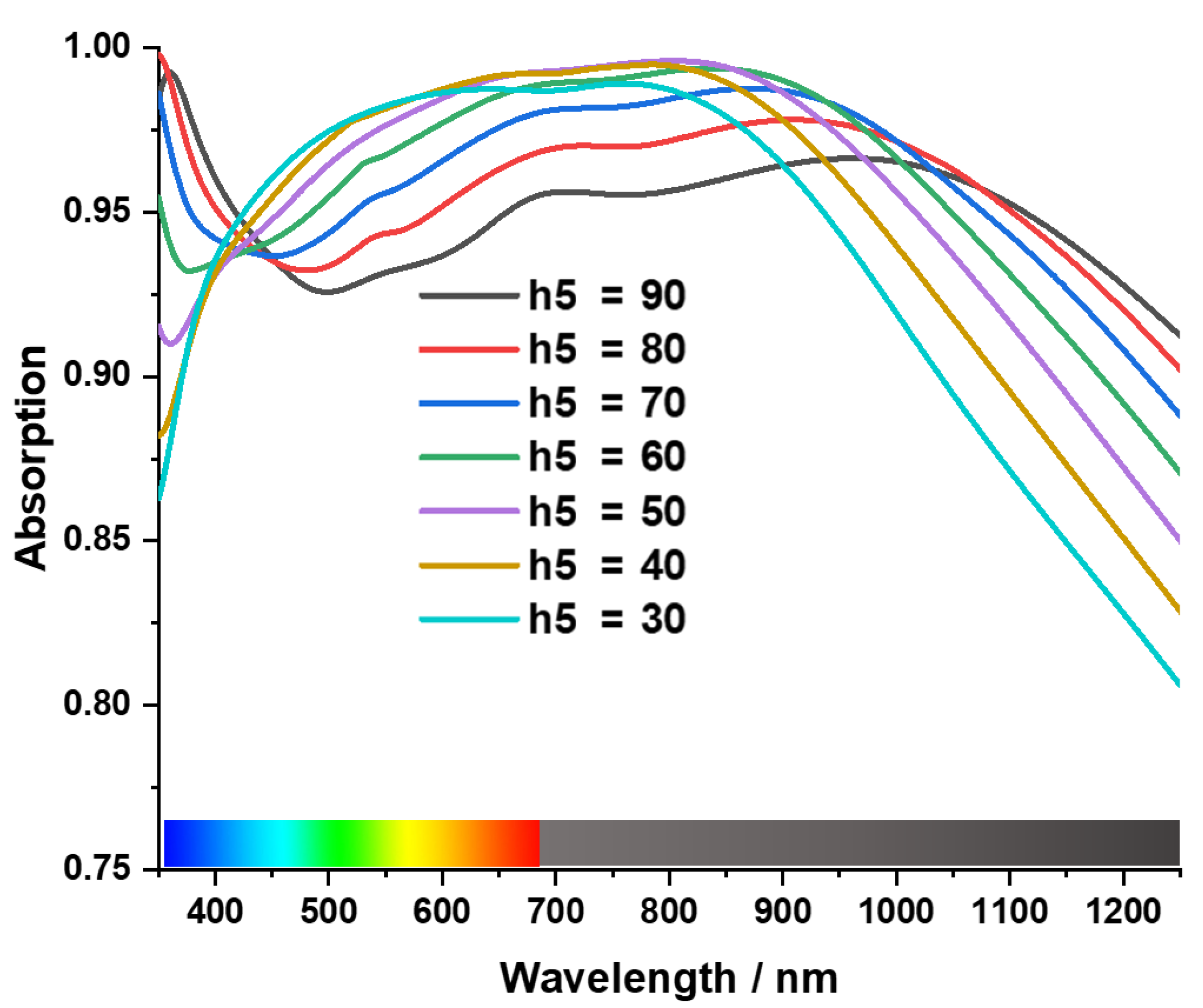
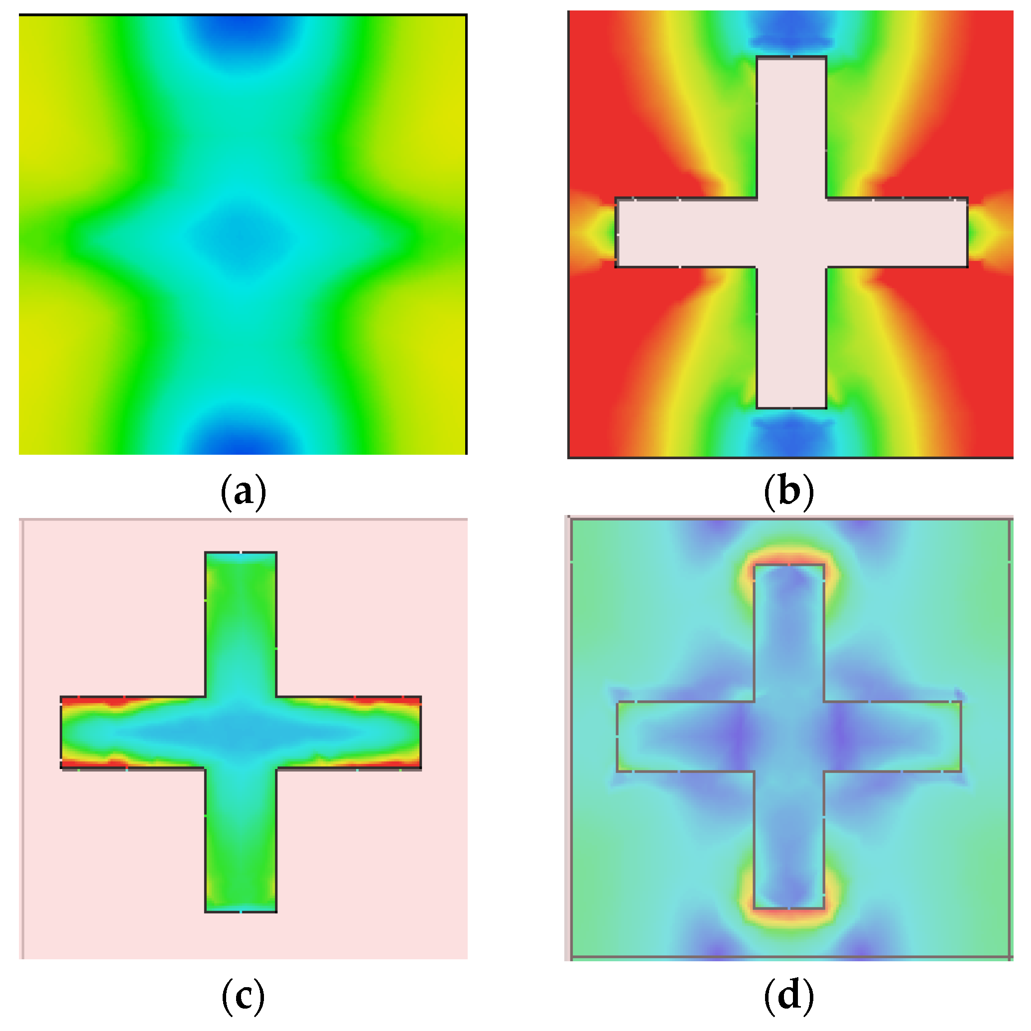
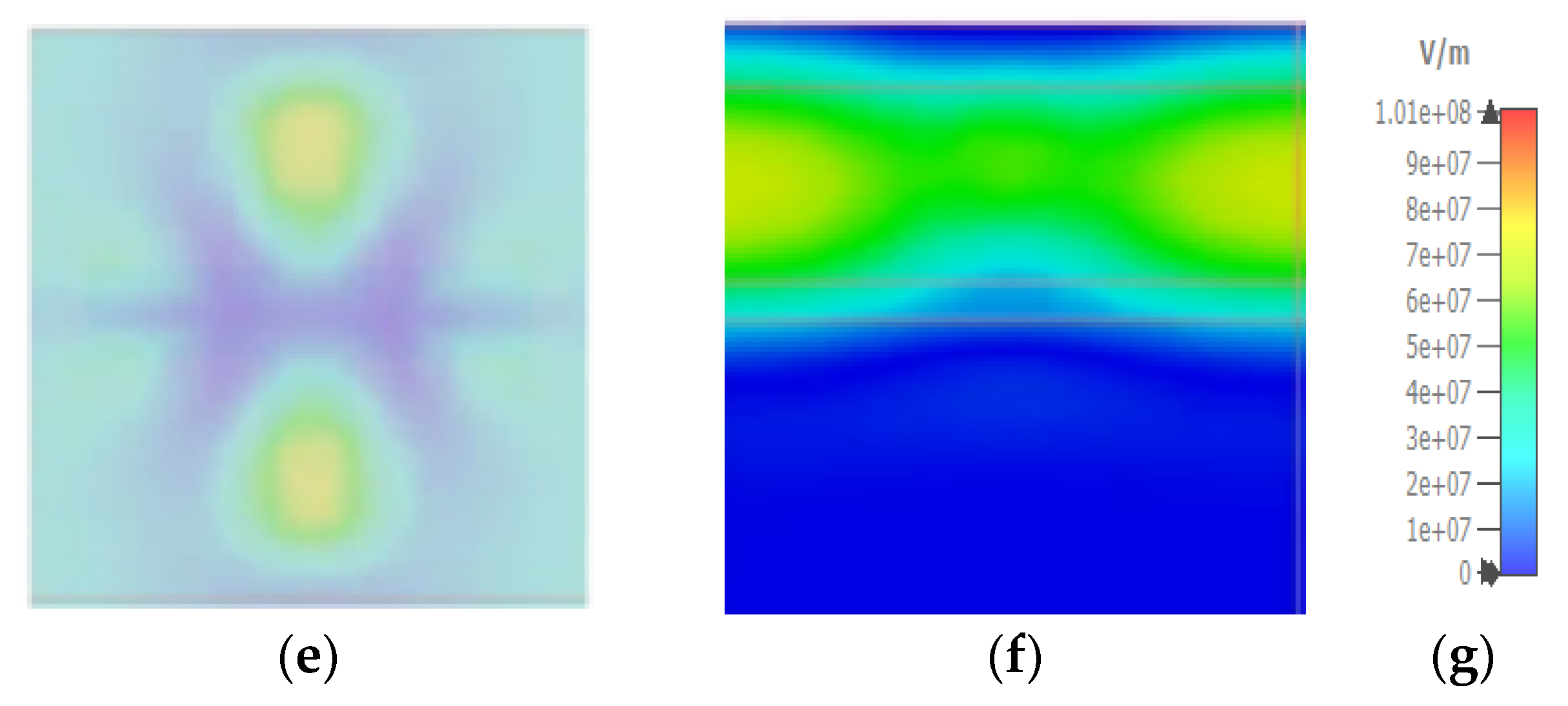
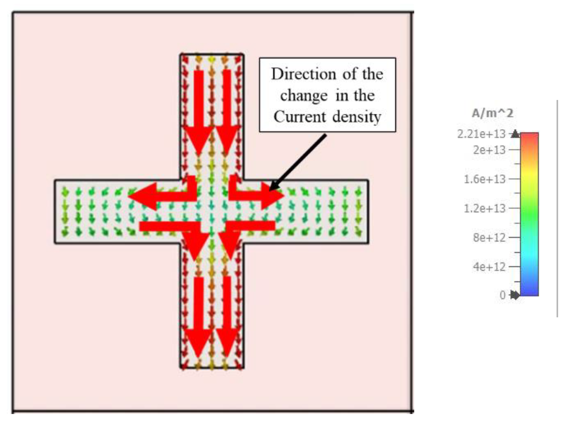
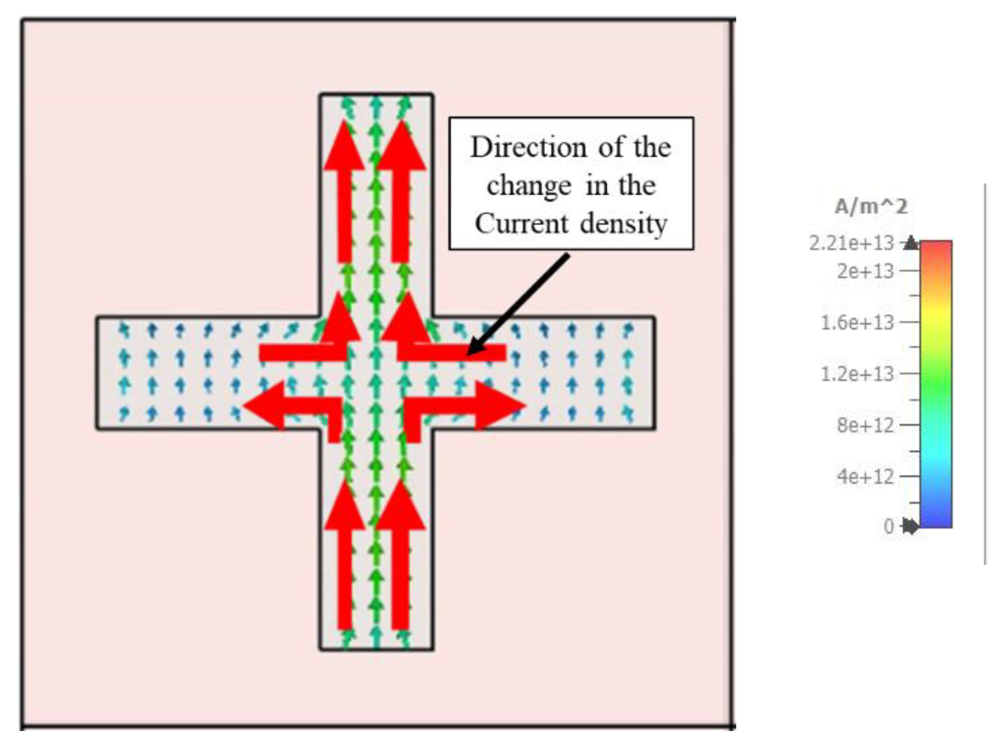
3. Result Analysis
4. Conclusions
Author Contributions
Funding
Data Availability Statement
Acknowledgments
Conflicts of Interest
References
- Liu, J.; Ma, W.-Z.; Chen, W.; Chen, Y.-S.; Deng, X.-C.; Gu, Y. A Metamaterial Absorber Based on Particle Swarm Optimization Suitable for Earth’s Atmospheric Transparency Window. IEEE Access 2021, 9, 92941–92951. [Google Scholar] [CrossRef]
- Landy, N.I.; Sajuyigbe, S.; Mock, J.J.; Smith, D.R.; Padilla, W.J. Perfect metamaterial absorber. Phys. Rev. Lett. 2008, 100, 207402. [Google Scholar] [CrossRef] [PubMed]
- Misran, N.; Yusop, S.H.; Islam, M.T.; Ismail, M.Y. Analysis of parameterization substrate thickness and permittivity for concentric split ring square reflectarray element. J. Kejuruter. J. Eng. 2012, 23, 11–16. [Google Scholar]
- Patel, S.K.; Parmar, J.; Katkar, V. Metasurface-based solar absorber with absorption prediction using machine learning. Opt. Mater. 2022, 124, 112049. [Google Scholar] [CrossRef]
- Shuvo, M.M.K.; Hossain, M.I.; Mahmud, S.; Rahman, S.; Topu, M.T.H.; Hoque, A.; Islam, S.S.; Soliman, M.S.; Almalki, S.H.A.; Islam, M.S.; et al. Polarization and angular insensitive bendable metamaterial absorber for UV to NIR range. Sci. Rep. 2022, 12, 4857. [Google Scholar] [CrossRef] [PubMed]
- Hoque, A.; Islam, M.T.; Almutairi, A.F.; Faruque, M.R.I. Design of split hexagonal patch array shaped nano-metaabsorber with ultra-wideband absorption for visible and UV spectrum application. Nanoscale Res. Lett. 2019, 14, 1–10. [Google Scholar] [CrossRef] [Green Version]
- Zhai, Y.; Ma, Y.; David, S.N.; Zhao, D.; Lou, R.; Tan, G.; Yang, R.; Yin, X. Scalable-manufactured randomized glass-polymer hybrid metamaterial for daytime radiative cooling. Science 2017, 355, 1062–1066. [Google Scholar] [CrossRef] [Green Version]
- Raman, A.P.; Anoma, M.A.; Zhu, L.; Rephaeli, E.; Fan, S. Passive radiative cooling below ambient air temperature under direct sunlight. Nature 2014, 515, 540–544. [Google Scholar] [CrossRef]
- Byrnes, S.J.; Blanchard, R.; Capasso, F. Harvesting renewable energy from Earth’s mid-infrared emissions. Proc. Natl. Acad. Sci. USA 2014, 111, 3927–3932. [Google Scholar] [CrossRef] [Green Version]
- Qu, Y.; Li, Q.; Cai, L.; Pan, M.; Ghosh, P.; Du, K.; Qiu, M. Thermal camouflage based on the phase-changing material GST. Light Sci. Appl. 2018, 7, 1–10. [Google Scholar] [CrossRef]
- Bao, H.-Y.; Wang, Y.-Z. Transient Invisibility and Cloak of Impact Elastic Wave in Piezoelectric/Piezomagnetic Metamaterials. AIAA J. 2022, 60, 65–75. [Google Scholar] [CrossRef]
- Alam, T.; Almutairi, A.F.; Samsuzzaman, M.; Cho, M.; Islam, M.T. Metamaterial array based meander line planar antenna for cube satellite communication. Sci. Rep. 2021, 11, 14087. [Google Scholar] [CrossRef] [PubMed]
- Ashraf, F.B.; Alam, T.; Islam, M.T.; Singh, M.J.; Misran, N.B.; Islam, M.T. Inkjet Printed Metamaterial Loaded Antenna for WLAN/WiMAX Applications. Comput. Mater. Contin. 2022, 71, 2271–2284. [Google Scholar] [CrossRef]
- Haxha, S.; AbdelMalek, F.; Ouerghi, F.; Charlton, M.; Aggoun, A.; Fang, X. Metamaterial superlenses operating at visible wavelength for imaging applications. Sci. Rep. 2018, 8, 16119. [Google Scholar] [CrossRef] [PubMed] [Green Version]
- Lu, F.; Tan, Q.; Ji, Y.; Guo, Q.; Guo, Y.; Xiong, J. A novel metamaterial inspired high-temperature microwave sensor in harsh environments. Sensors 2018, 18, 2879. [Google Scholar] [CrossRef] [PubMed] [Green Version]
- Hakim, M.L.; Alam, T.; Almutairi, A.F.; Mansor, M.F.; Islam, M.T. Polarization insensitivity characterization of dual-band perfect metamaterial absorber for K band sensing applications. Sci. Rep. 2021, 11, 17829. [Google Scholar] [CrossRef]
- Hakim, M.L.; Alam, T.; Soliman, M.S.; Sahar, N.M.; Baharuddin, M.H.; Almalki, S.H.A.; Islam, M.T. Polarization insensitive symmetrical structured double negative (DNG) metamaterial absorber for Ku-band sensing applications. Sci. Rep. 2022, 12, 479. [Google Scholar] [CrossRef]
- Cheng, Y.; Zhang, H.; Mao, X.S.; Gong, R. Dual-band plasmonic perfect absorber based on all-metal nanostructure for refractive index sensing application. Mater. Lett. 2018, 219, 123–126. [Google Scholar] [CrossRef]
- Hoque, A.; Islam, M.T.; Almutairi, A.F.; Alam, T.; Singh, M.J.; Amin, N. A polarization independent quasi-TEM metamaterial absorber for X and Ku band sensing applications. Sensors 2018, 18, 4209. [Google Scholar] [CrossRef] [Green Version]
- Hengbo, X. Design, simulation, and measurement of a multiband tunable metamaterial filter. Opt. Mater. 2022, 127, 112253. [Google Scholar] [CrossRef]
- Ozturk, M.; Sevim, U.K.; Akgol, O.; Unal, E.; Karaaslan, M. Determination of physical properties of concrete by using microwave nondestructive techniques. Appl. Comput. Electromagn. Soc. J. 2018, 46, 265–272. [Google Scholar]
- Veselago, V.G. The electrodynamics of substances with simultaneously negative values of img align = absmiddle Alt = ϵ Eps/Img and μ. Phys.-Uspekhi 1968, 10, 509–514. [Google Scholar] [CrossRef]
- Smith, D.R.; Padilla, W.J.; Vier, D.; Nemat-Nasser, S.C.; Schultz, S. Composite medium with simultaneously negative permeability and permittivity. Phys. Rev. Lett. 2000, 84, 4184. [Google Scholar] [CrossRef] [PubMed] [Green Version]
- Salim, A.; Lim, S. Review of recent metamaterial microfluidic sensors. Sensors 2018, 18, 232. [Google Scholar] [CrossRef] [PubMed] [Green Version]
- Lee, Y.; Kim, S.-J.; Park, H.; Lee, B. Metamaterials and metasurfaces for sensor applications. Sensors 2017, 17, 1726. [Google Scholar] [CrossRef] [Green Version]
- Wang, Y.; Sun, T.; Paudel, T.; Zhang, Y.; Ren, Z.; Kempa, K. Metamaterial-plasmonic absorber structure for high efficiency amorphous silicon solar cells. Nano Lett. 2012, 12, 440–445. [Google Scholar] [CrossRef]
- Amiri, M.; Tofigh, F.; Shariati, N.; Lipman, J.; Abolhasan, M. Review on metamaterial perfect absorbers and their applications to IoT. IEEE Internet Things J. 2020, 8, 4105–4131. [Google Scholar] [CrossRef]
- Kim, H.K.; Lee, D.; Lim, S. A fluidically tunable metasurface absorber for flexible large-scale wireless ethanol sensor applications. Sensors 2016, 16, 1246. [Google Scholar] [CrossRef] [PubMed] [Green Version]
- Mou, N.; Liu, X.; Wei, T.; Dong, H.; He, Q.; Zhou, L.; Zhang, Y.; Zhang, L.; Sun, S. Large-scale, low-cost, broadband and tunable perfect optical absorber based on phase-change material. Nanoscale 2020, 12, 5374–5379. [Google Scholar] [CrossRef]
- Xiao, D.; Zhu, M.; Sun, L.; Zhao, C.; Wang, Y.; Teo, E.H.T.; Hu, F.; Tu, L. Flexible ultra-wideband terahertz absorber based on vertically aligned carbon nanotubes. ACS Appl. Mater. Interfaces 2019, 11, 43671–43680. [Google Scholar] [CrossRef]
- Ruan, J.; Ji, S.; Tao, Z.; Lan, F. Ultra-wideband metamaterial absorber doped GaAs in the infrared region. J. Electromagn. Waves Appl. 2021, 35, 1088–1098. [Google Scholar] [CrossRef]
- Charola, S.; Patel, S.K.; Dalsaniya, K.; Jadeja, R.; Nguyen, T.K.; Dhasarathan, V. Numerical investigation of wideband L-shaped metasurface based solar absorber for visible and ultraviolet region. Phys. B Condens. Matter 2021, 601, 412503. [Google Scholar] [CrossRef]
- Wu, B.; Liu, Z.; Du, G.; Chen, Q.; Liu, X.; Fu, G.; Liu, G. Polarization and angle insensitive ultra-broadband mid-infrared perfect absorber. Phys. Lett. A 2020, 384, 126288. [Google Scholar] [CrossRef]
- Liang, Y.; Lin, H.; Lin, S.; Wu, J.; Li, W.; Meng, F.; Yang, Y.; Huang, X.; Jia, B.; Kivshar, Y. Hybrid anisotropic plasmonic metasurfaces with multiple resonances of focused light beams. Nano Lett. 2021, 21, 8917–8923. [Google Scholar] [CrossRef]
- Song, Q.; Zhang, W.; Wu, P.C.; Zhu, W.; Shen, Z.X.; Chong, P.H.J.; Liang, Q.X.; Yang, Z.C.; Hao, Y.L.; Cai, H.; et al. Water-Resonator-Based Metasurface: An Ultrabroadband and Near-Unity Absorption. Adv. Opt. Mater. 2017, 5, 1601103. [Google Scholar] [CrossRef]
- Zhang, W.; Zhu, W.M.; Chia, E.E.M.; Shen, Z.X.; Cai, H.; Gu, Y.D.; Ser, W.; Liu, A.Q. A pseudo-planar metasurface for a polarization rotator. Opt. Express 2014, 22, 10446–10454. [Google Scholar] [CrossRef]
- Zhang, M.; Zhang, W.; Liu, A.; Li, F.; Lan, C. Tunable polarization conversion and rotation based on a reconfigurable metasurface. Sci. Rep. 2017, 7, 12068. [Google Scholar] [CrossRef] [Green Version]
- Aydin, K.; Ferry, V.E.; Briggs, R.M.; Atwater, H.A. Broadband polarization-independent resonant light absorption using ultrathin plasmonic super absorbers. Nat. Commun. 2011, 2, 517. [Google Scholar] [CrossRef]
- Wang, Y.; Xuan, X.-F.; Zhu, L.; Yu, H.-J.; Gao, Q.; Ge, X.-L. Numerical study of an ultra-broadband, wide-angle, polarization-insensitive absorber in visible and infrared region. Opt. Mater. 2021, 114, 110902. [Google Scholar] [CrossRef]
- Yang, J.; Xu, C.; Qu, S.; Ma, H.; Wang, J.; Pang, Y. Optical transparent infrared high absorption metamaterial absorbers. J. Adv. Dielectr. 2018, 8, 1850007. [Google Scholar] [CrossRef] [Green Version]
- Wang, B.X.; Zhai, X.; Wang, G.Z.; Huang, W.Q.; Wang, L.L. A novel dual-band terahertz metamaterial absorber for a sensor application. J. Appl. Phys. 2015, 117, 014504. [Google Scholar] [CrossRef]
- D.C. AG. CST Studio Suite. Available online: https://www.3ds.com/products-services/simulia/products/cst-studio-suite/ (accessed on 10 April 2022).
- Malitson, I.H. Interspecimen comparison of the refractive index of fused silica. Josa 1965, 55, 1205–1209. [Google Scholar] [CrossRef]
- Wu, D.; Liu, C.; Xu, Z.; Liu, Y.; Yu, Z.; Yu, L.; Chen, L.; Li, R.; Ma, R.; Ye, H. The design of ultra-broadband selective near-perfect absorber based on photonic structures to achieve near-ideal daytime radiative cooling. Mater. Des. 2018, 139, 104–111. [Google Scholar] [CrossRef]
- Weaver, J.; Olson, C.; Lynch, D.W. Optical properties of crystalline tungsten. Phys. Rev. B 1975, 12, 1293. [Google Scholar] [CrossRef] [Green Version]
- Shahsafi, A.; Xiao, Y.; Salman, J.; Gundlach, B.S.; Wan, C.; Roney, P.J.; Kats, M.A. Mid-infrared optics using dielectrics with refractive indices below unity. Phys. Rev. Appl. 2018, 10, 034019. [Google Scholar] [CrossRef] [Green Version]
- Li, Y.; Li, L.; Wang, F.; Ge, H.; Xie, R.; An, B. Two broad absorption bands in infrared atmosphere transparent windows by trapezoid multilayered grating. Opt. Mater. Express 2020, 10, 682–692. [Google Scholar] [CrossRef]
- Zhi, T.; Tao, T.; Liu, B.; Yu, Y.; Xie, Z.; Zhao, H.; Chen, D. High Performance Wide Angle DBR Design for Optoelectronic Devices. IEEE Photonics J. 2021, 13, 1–6. [Google Scholar] [CrossRef]
- Cui, Y.; Fung, K.H.; Xu, J.; Ma, H.; Jin, Y.; He, S.; Fang, N.X. Ultrabroadband light absorption by a sawtooth anisotropic metamaterial slab. Nano Lett. 2012, 12, 1443–1447. [Google Scholar] [CrossRef] [Green Version]
- Wang, B.-X.; Xu, W.; Wu, Y.; Yang, Z.; Lai, S.; Lu, L. Realization of multiple-band terahertz metamaterial absorber using two identical split rings having opposite opening directions connected by a rectangular patch. Nanoscale Adv. 2022, 4, 1359–1367. [Google Scholar] [CrossRef]
- Jin, G.; Zhou, T.; Tang, B. Ultra-Narrowband Anisotropic Perfect Absorber Based on α-MoO3 Metamaterials in the Visible Light Region. Nanomaterials 2022, 12, 1375. [Google Scholar] [CrossRef]
- Hakim, M.L.; Alam, T.; Islam, M.S.; Salaheldeen, M.M.; Almalki, S.; Baharuddin, M.H.; Alsaif, H.; Islam, M.T. Wide-Oblique-Incident-Angle Stable Polarization-Insensitive Ultra-Wideband Metamaterial Perfect Absorber for Visible Optical Wavelength Applications. Materials 2022, 15, 2201. [Google Scholar] [CrossRef] [PubMed]


| Symble | Parameter Value (nm) | Symble | Parameter Value (nm) |
|---|---|---|---|
| W1 | 200 | h2 | 12.5 |
| W2 | 157.20 | h3 | 68 |
| W3 | 31.5 | h4 | 21 |
| h1 | 105 |
| Ref. | Operating Band (THz) | WL- nm | Avg. Absorption | Polarization Independency Angular Stability | Materials | No. of Layer | Dimension (Length × Width × Height) |
|---|---|---|---|---|---|---|---|
| [29] | 300–516 | 580–1000 | 95.2% | Independent, θ = 0° | Ge2, Sd2, Te5 | 2 | 0.4λ × 0.4λ × 0.21λ |
| [30] | 0.1–3 | 2.9 × 10⁶–9.993 × 10⁴ | 87.09% | Independent, θ = 0° | Cu, Si | 4 | 5λ × 5λ × 0.15λ |
| [27] | 21–37 | 8000–14,000 | 95% | Independent | Ti, Si | 5 | 0.3λ × 0.3 λ × 0.1λ |
| [40] | 24.58–28.82 | 10,000–12,000 | 88% | Independent, θ = ≤50° | In2SnO5, ZnS | 4 | 0.8 λ × 0.8 λ × 0.055 λ |
| [31] | 80–160 | 1800–3700 | 98% | Independent, θ = ≤45° | GaSa, FR-4, Cu | 4 | 5λ × 5λ × 0.4λ |
| [32] | 428–1070 | 280–700 | 90% | Independent, θ = ≤30° | Tungsten, SiO2 | 3 | 2λ × 2λ × 0.4λ |
| [30] | 100–666 | 450–3000 | 98% | Independent, | Fe, Si, Au | 3 | 0.6λ × 0.6λ × 2λ |
| [1] | 220–360 | 2000–6000 | 89% | Independent, θ = ≤35° | Cu, GaAs | 4 | 0.77λ × 0.77λ × 0.11λ |
| [52] | 428–750 | 300–700 | 92.2% | Independent θ = ≤70° | Tungsten, SiO2 | 3 | 3.2 λ × 3.2λ × 0.77λ |
| [38] | 430–750 | 400–700 | 71% | Independent θ = ≤45° | Ag, SiO2 | 3 | 0.75 λ × 0.75 λ × 0.65 λ |
| Proposed MA | 240–856 | 350–1250 | 95.3% | Independent θ = ≤45° | Tungsten, SiO2 | 4 | 0.57λ × 0.57λ × 0.59λ |
Publisher’s Note: MDPI stays neutral with regard to jurisdictional claims in published maps and institutional affiliations. |
© 2022 by the authors. Licensee MDPI, Basel, Switzerland. This article is an open access article distributed under the terms and conditions of the Creative Commons Attribution (CC BY) license (https://creativecommons.org/licenses/by/4.0/).
Share and Cite
Musa, A.; Hakim, M.L.; Alam, T.; Islam, M.T.; Alshammari, A.S.; Mat, K.; M., M.S.; Almalki, S.H.A.; Islam, M.S. Polarization Independent Metamaterial Absorber with Anti-Reflection Coating Nanoarchitectonics for Visible and Infrared Window Applications. Materials 2022, 15, 3733. https://doi.org/10.3390/ma15103733
Musa A, Hakim ML, Alam T, Islam MT, Alshammari AS, Mat K, M. MS, Almalki SHA, Islam MS. Polarization Independent Metamaterial Absorber with Anti-Reflection Coating Nanoarchitectonics for Visible and Infrared Window Applications. Materials. 2022; 15(10):3733. https://doi.org/10.3390/ma15103733
Chicago/Turabian StyleMusa, Ahmad, Mohammad Lutful Hakim, Touhidul Alam, Mohammad Tariqul Islam, Ahmed S. Alshammari, Kamarulzaman Mat, M. Salaheldeen M., Sami H. A. Almalki, and Md. Shabiul Islam. 2022. "Polarization Independent Metamaterial Absorber with Anti-Reflection Coating Nanoarchitectonics for Visible and Infrared Window Applications" Materials 15, no. 10: 3733. https://doi.org/10.3390/ma15103733