Article

Improved Electrical Characteristics of Gallium Oxide/P-Epi Silicon Carbide Static Induction Transistors with UV/Ozone Treatment Fabricated by RF Sputter

1
Department of Electronic Materials Engineering, Kwangwoon University, 20 Kwangwoon-ro, Nowon-gu, Seoul 01897, Korea
2
Department of Electronic Materials Engineering, Nagoya Institute of Technology, Gokiso-cho, Showa-ku, Nagoya, Aichi 466-8555, Japan
*
Author to whom correspondence should be addressed.
Materials 2021, 14(5), 1296; https://doi.org/10.3390/ma14051296
Submission received: 30 December 2020 / Revised: 26 February 2021 / Accepted: 27 February 2021 / Published: 8 March 2021

Abstract

:
In this study, static induction transistors (SITs) with beta gallium oxide (β-Ga2O3) channels are grown on a p-epi silicon carbide (SiC) layer via radio frequency sputtering. The Ga2O3 films are subjected to UV/ozone treatment, which results in reduced oxygen vacancies in the X-ray photoelectron spectroscopy data, lower surface roughness (3.51 nm) and resistivity (319 Ω·cm), and higher mobility (4.01 cm2V−1s−1). The gate leakage current is as low as 1.0 × 10⁻¹¹ A at VGS = 10 V by the depletion layer formed between n-Ga2O3 and p-epi SiC at the gate region with a PN heterojunction. The UV/O3-treated SITs exhibit higher (approximately 1.64 × 10² times) drain current (VDS = 12 V) and on/off ratio (4.32 × 10⁵) than non-treated control devices.

1. Introduction

Among the different polytypes of Ga2O3 (α, β, γ, δ, and ε), monoclinic Ga2O3 is the most thermally stable and can be obtained by annealing sputtered films [1,2,3,4] because metastable Ga2O3 can be subsequently converted into β-Ga2O3 after high-temperature annealing. Gallium oxide (Ga2O3) is a wide-bandgap material with an energy gap (Eg) of 4.8–5.1 eV and has drawn considerable attention for use in various applications such as high-powered semiconductor devices, ultra-violet (UV) detectors, and gas and fire sensors [5,6,7,8,9,10]. In addition, it exhibits an n-type conductivity that does not require intentional doping due to inherent oxygen vacancies in the grown crystal, as in the case of ZnO or InGaZnO (IGZO) [11,12]. To improve rectification or bipolar device elements in Ga2O3, an n-type Ga2O3 film should be grown on a p-type substrate.
4-H silicon carbide (SiC) is a wide-bandgap material (Eg ~ 3.26 eV) that clearly shows a higher value of thermal conductivity (~370 W/m·K) than those of Ga2O3 (~27 W/m·K) and GaN (~177 W/m·K). The maturity of the bulk SiC substrate technology and optimized device processing makes it one of the most desirable candidates for a p-type doped counterpart to form heterojunctions with Ga2O3 and other materials [13,14,15,16].
Some studies have reported the electron mobility and crystalline quality of Ga2O3 grown on GaN substrates [17]. The static induction transistor (SIT) is a short-channel field effect transistor that typically displays unsaturated output characteristics [18] and shows potential for use in high frequency and high-powered applications. Consequently, SIT devices could be used for driver circuits such as in switching mode power supplies (SMPS) [19]. Furthermore, Ga2O3 SIT structures have been formed by using GaN, which exhibits a significant level of gate leakage current [20,21]. This may be controlled by employing a reliable PN heterojunction gate element.
The lattice constants of β-Ga2O3, a = 12.23 Å, b = 3.04 Å, c = 5.80 Å, and β = 103.7°, result in a lattice mismatch of ~2.63% between the c-plane GaN and β-Ga2O3 [22]. Note that the lattice mismatch between β-Ga2O3 grown on a 4H-SiC wafer (a = 3.10 Å and c = 10.53 Å) can become as low as 3.22%. 4H-SiC can be selected as a growth substrate not only because it has a low lattice mismatch with Ga2O3 but also because of its high inertness and high thermal conductivity [18].
So far, there have been only limited reports on Ga2O3/SiC structures, which mostly focus on simple diode structures [23]. Thus, it is important to realize reliable heterojunction device structures of Ga2O3 and other p-type doped materials.
In this work, we demonstrate SITs fabricated by depositing n-type Ga2O3 on an epitaxially grown layer of p-type 4H-SiC on an n-type 4H-SiC substrate. The PN heterojunction gate of the SIT forms a depletion layer with a proper gate bias, thereby controlling the Ga2O3 channel. Our specific goal was to examine the control of gate leakage current through a PN heterojunction gate and the influence of UV/ozone (UV/O3) treatment on the performance of SITs.

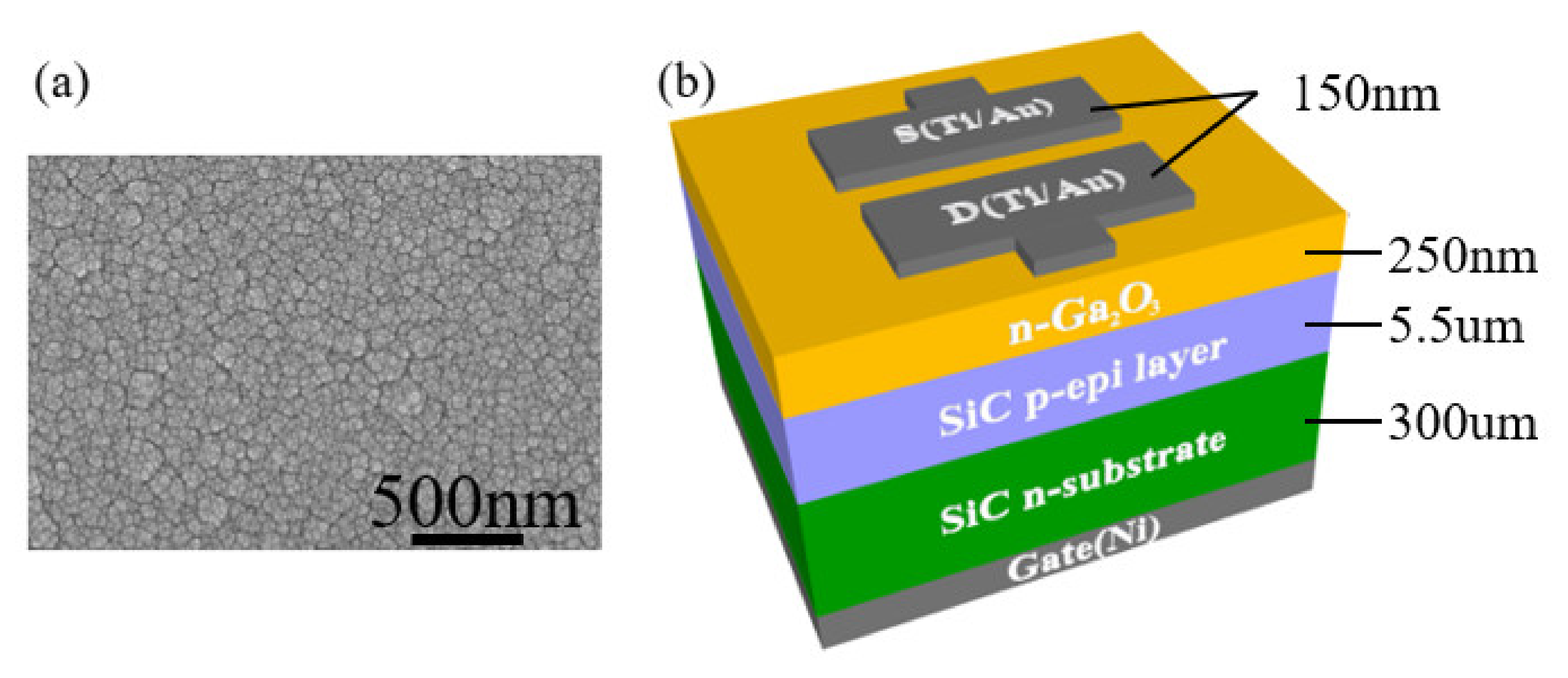
2. Materials and Methods

We used a 4H-SiC wafer with a layer of epitaxially grown 4H-SiC (p-type) on highly doped n-type 4H-SiC. After radio corporation of america (RCA) cleaning the SiC wafer with SPM solution (H2SO4:H2O2 = 4:1), we removed the native silicon dioxide (SiO2) layer using a buffered oxide etch (BOE) solution. The 150 nm gate nickel film was deposited by E-beam evaporator. The samples were annealed at 1050 °C in N2 gas for 1 min by rapid thermal annealing (RTA) to form an ohmic contact with nickel silicide. Ga2O3 films were deposited by radio frequency (RF) sputtering of a Ga2O3 (99.99% purity) target. Films of 250 nm were grown on the epitaxial 4H-SiC layer under 35 mTorr at a pure argon mass flow rate of 4 sccm. After deposition, SiC wafers with Ga2O3 film were annealed at 800 °C for 40 min under N2. The Ga2O3 thin film doping concentration is ~3.27 × 1015 cm−3, with a resistivity of ~7.39 Ω·cm as measured by hall measurement as confirmed. The Ga2O3 films were illuminated by UV/O3 exposure for comparison with samples, depending on the treatment. Shown in Figure 1, Ti (50 nm) and Au (100 nm) metal was deposited on the Ga2O3 layer under 6 × 10⁻² mTorr by E-beam evaporation. The gold layer was applied to prevent the oxidation of the titanium. After Ti/Au-deposition, the samples were annealed at 300 °C for 30 min to from ohmic contacts.
The SIT consisting of deposited Ga2O3 on 4H-SiC (doping concentration ~5 × 1016cm−3) was investigated and the manufactured devices were exposed to UV/O3 for varying durations to improve the Ga2O3 film quality. We used an AHTECH AH-1700 UV ozone cleaner to remove contamination with a wavelength 184 nm and 254 nm. The material properties of Ga2O3 were characterized by atomic force microscopy (AFM), X-ray photoelectron spectroscopy (XPS), and Hall measurements with UV/O3 treatment for different times. ID-VD and ID/G-VG measurements were obtained and analyzed. The gate voltage-dependent operation of static induction devices will be discussed in the following section.

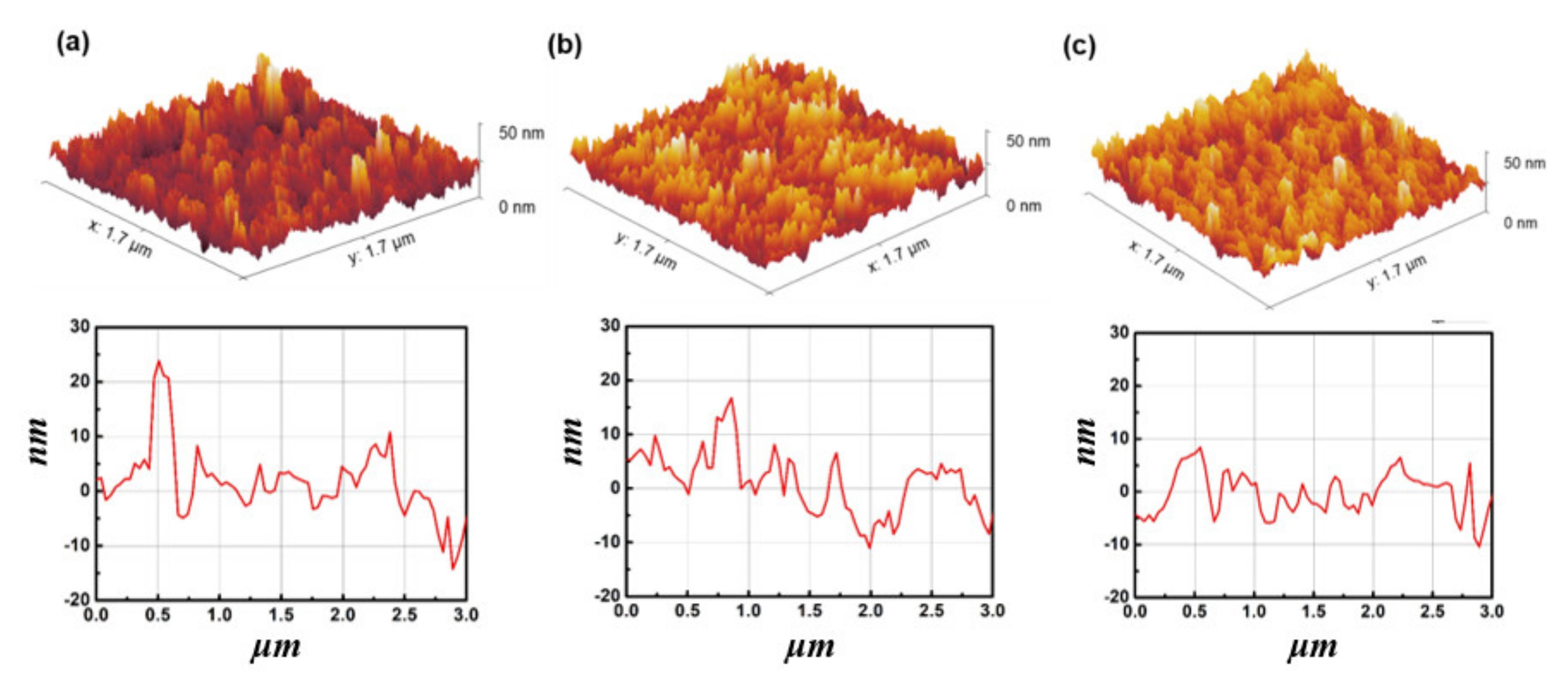
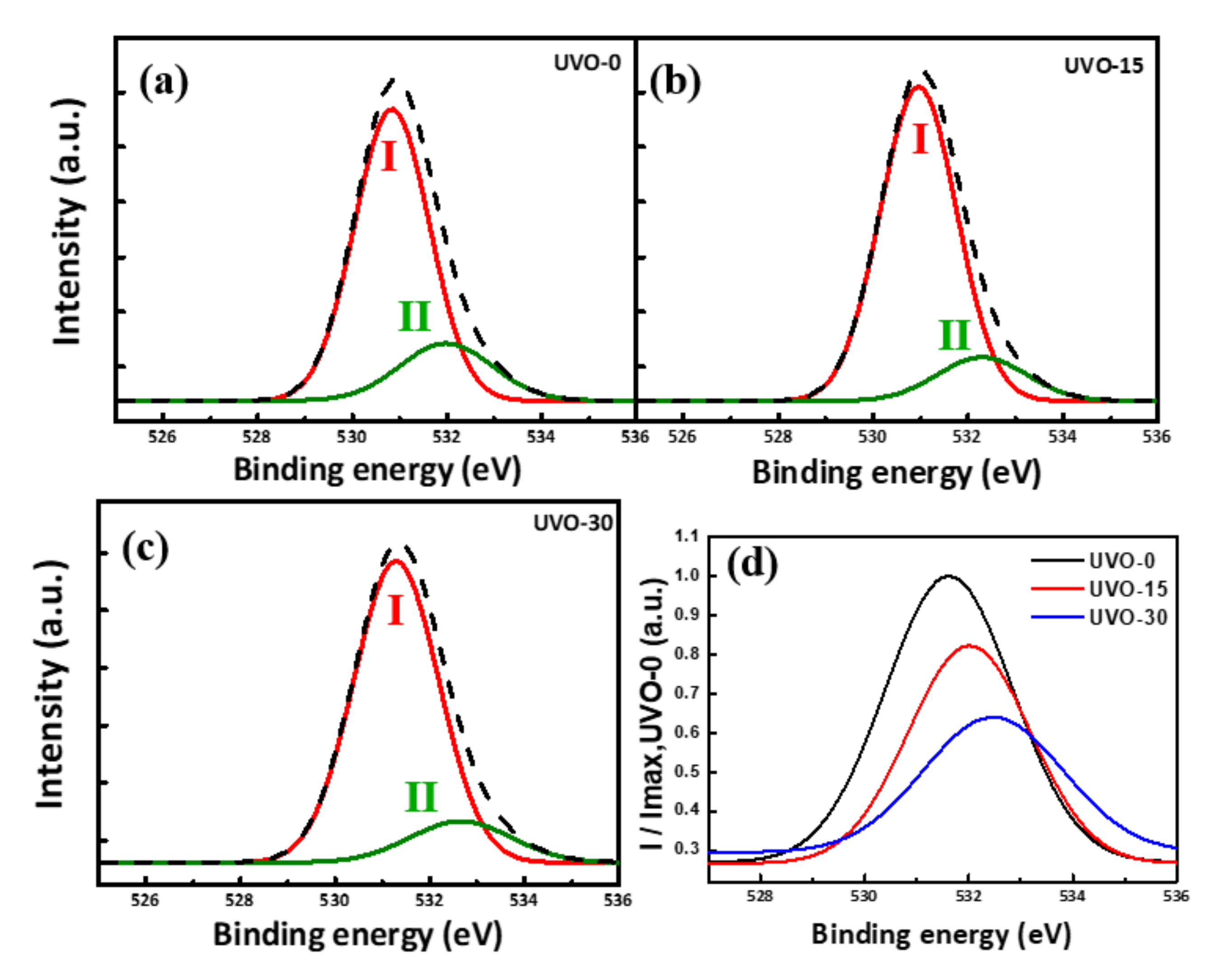
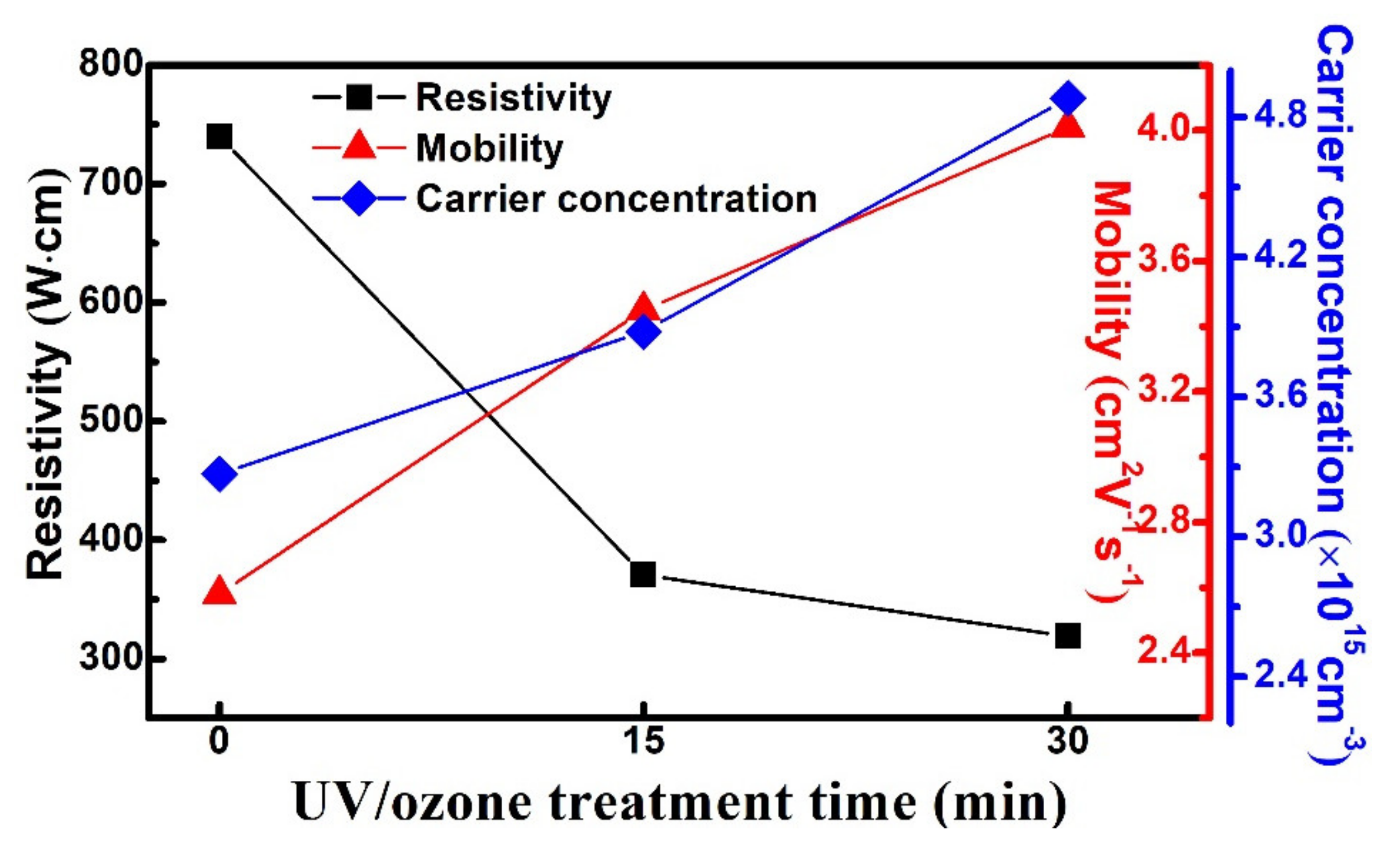
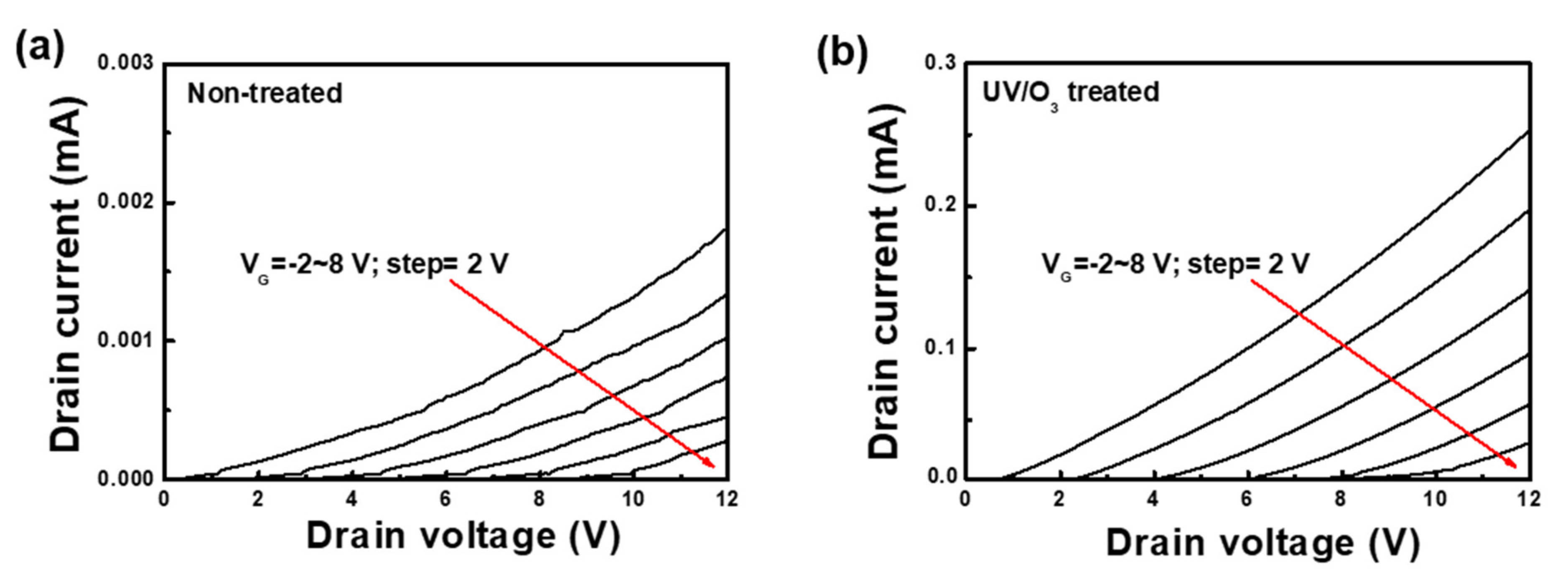
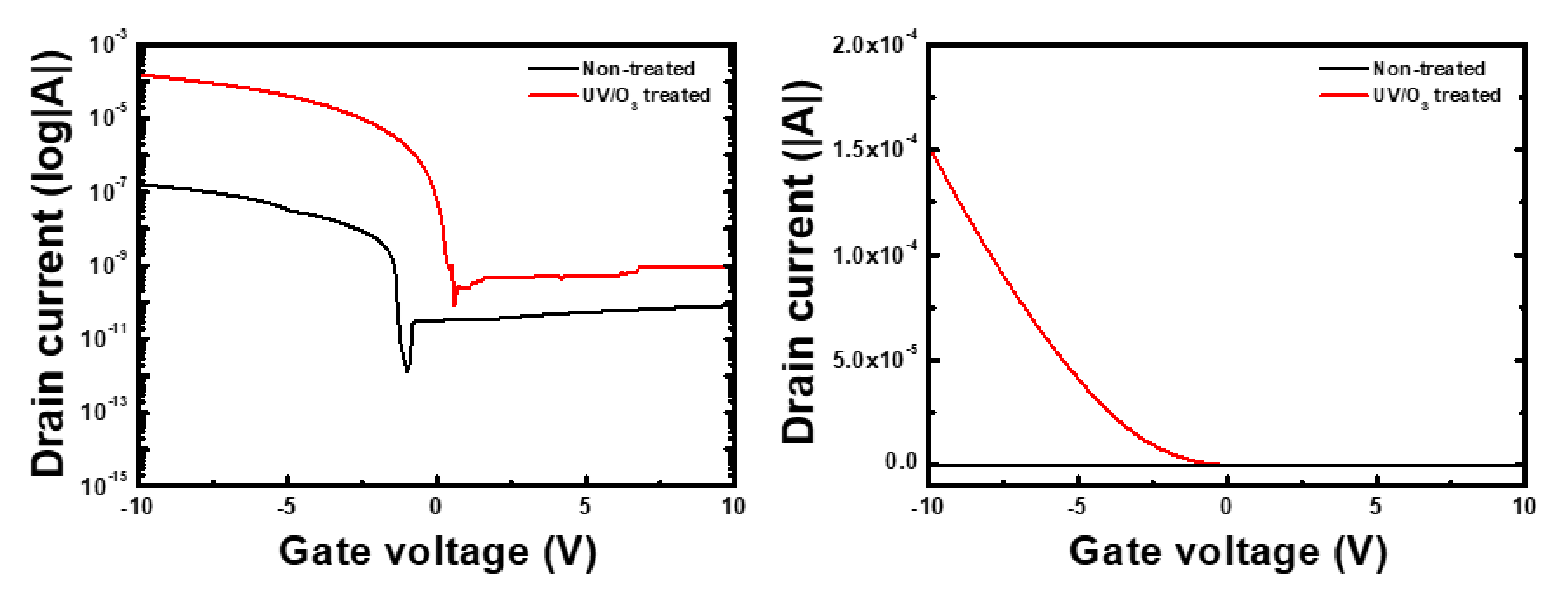
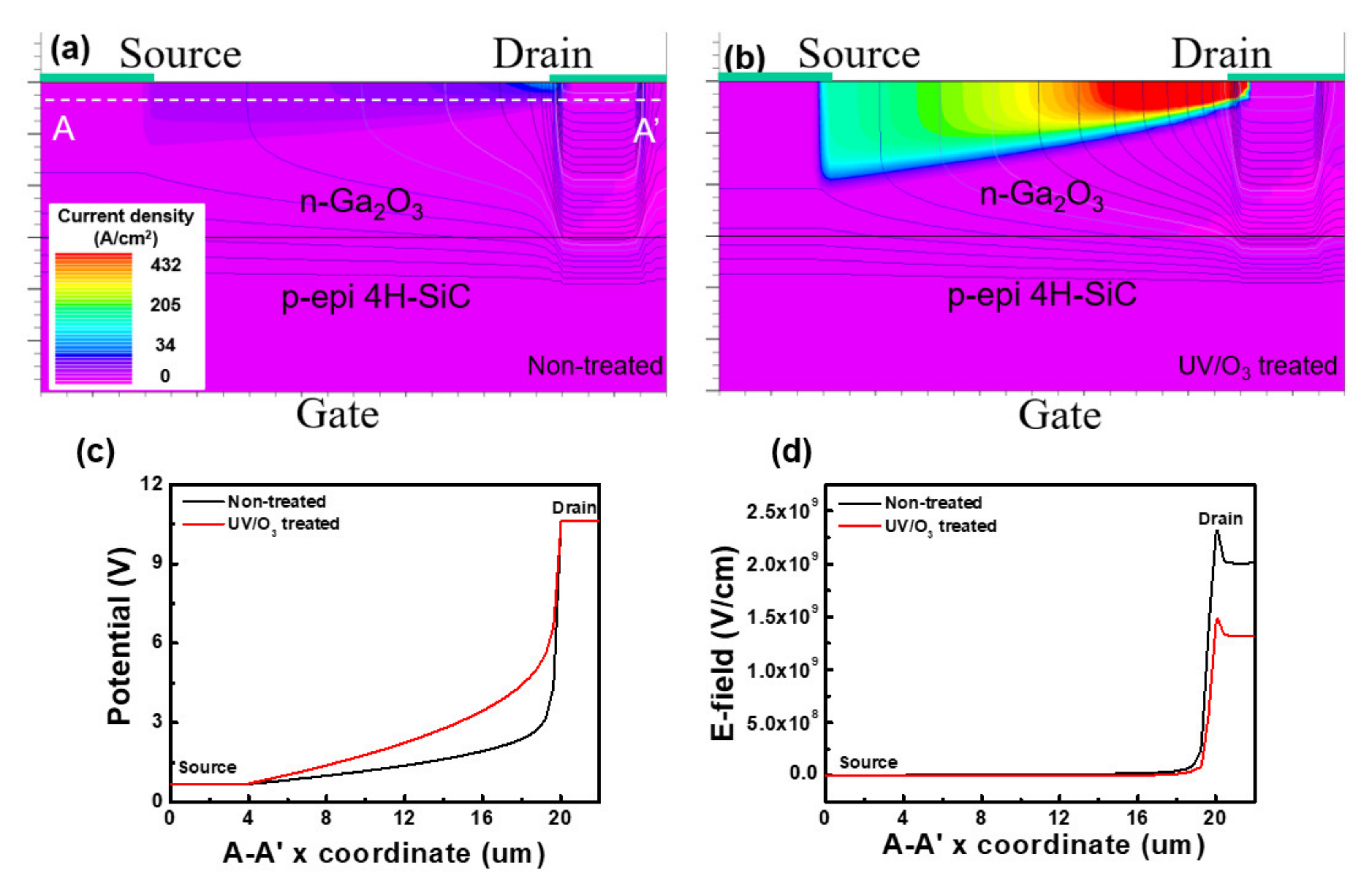
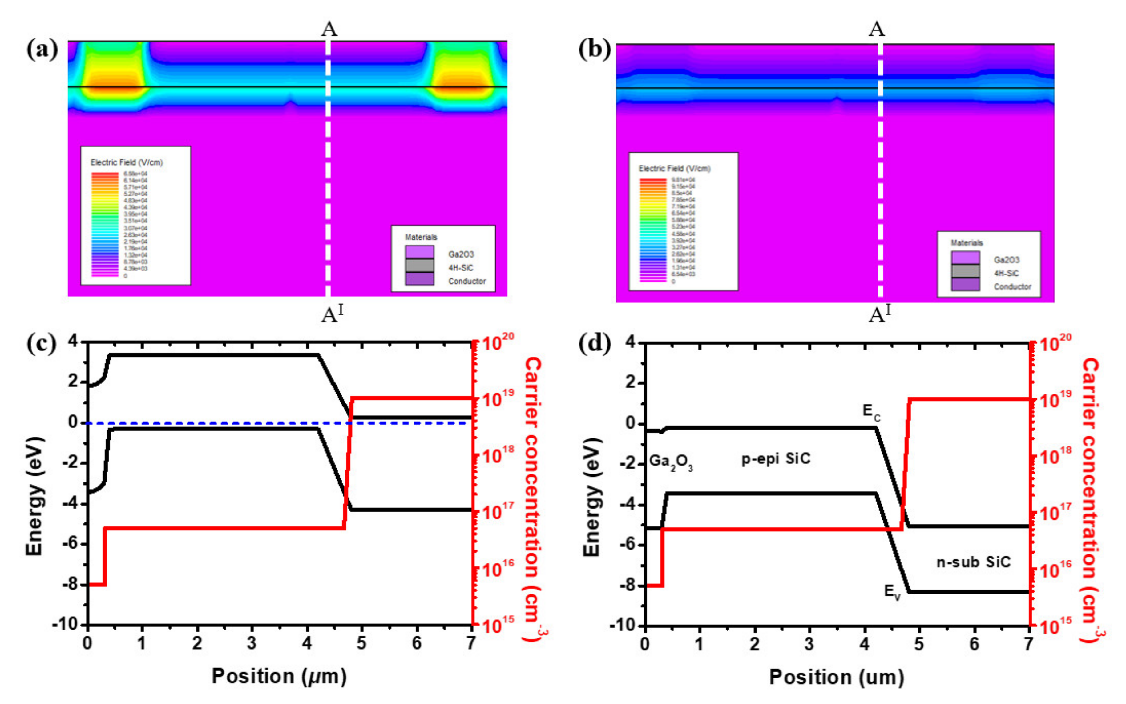
3. Results and Discussion

Figure 2a–c shows that the surface roughness of the films became smoother as the exposure time increased from 0 to 15 to 30 min; the root-mean-square (RMS) values were 5.23, 4.24, and 3.51 nm, respectively. The light energies at wavelengths of 185 nm and 254 nm energy were larger than contamination bonding energies. Therefore contaminants or organic materials could be removed through UV/O3 treatment [24]. If the UV/O3 treatment is applied for more than 30 min, the further benefits of the treatment are small [24]. This observation suggests that UV/O3 treatment can remove the contamination and organic residue resulting from oxygen radicals [25,26].
The bulk and surface defects, which can be observed as surface roughness and oxygen vacancies, may affect the performance of oxide semiconductor devices. During the UV/O3 treatment, long-wavelength UV radiation was absorbed by the ozone and decomposed this to form highly reactive atomic oxygen. The atomic oxygen in turn reacted with oxygen vacancies in the thin film, thereby reducing the number of charge carrier traps. The O 1s core-level X-ray photoelectron spectroscopy (XPS) profiles shown in Figure 3 exhibit peaks centered at 528.9 eV (OI), which indicate that O2 ions bonded with Ga atoms, forming Ga2O3. It is desirable to maximize metal–oxygen–metal (M-O-M) bonding in an oxide semiconducting layer, which may result in decreased oxygen vacancies. The comparison of the XPS O1s subpeaks is therefore important to understand the behavior. The high M-O-M peaks in the XPS data show that the carrier transport property of the film may have been improved as to the carrier transport properties. The decrease in the oxygen vacancies may have resulted in easier electron transition from the valance band to the conduction band due to the special electron configuration of 3d104p1 [27]. The peak with a binding energy of 530.3 eV (OII) is associated with the oxygen-deficient regions on the surface of the Ga2O3 films, which represent the quantity of related oxygen vacancies. Whereas it is possible that further electron states may have made small contributions to the observed O 1s spectra in Figure 3a–c, the extracted OII peaks in (d) describe the relative contribution of the OII states. As shown in Figure 3d the oxygen vacancy peak (OII) was reduced by UV/O3 treatment. The magnitudes of the OII peaks of the devices treated with UV/O3 for 15 min and 30 min were at 80% and 60% of the OII peak magnitude of the untreated sample device, respectively. The decreased oxygen vacancies led to a high Ion/Ioff ratio, mobility, and unintentional doping concentrations.
Hall effect measurements were performed at room temperature to determine the electrical parameters of the Ga2O3 films on 4H-SiC. Figure 4 shows the Hall mobility, carrier concentration, and resistivity of the deposited Ga2O3 films on 4H-SiC as a function of the UV/O3 treatment time. The resistivity of Ga2O3 films decreased from 740 to 319 Ω·cm as the UV/O3 treatment time increased. The mobility and n-type carrier concentration increased from 2.58 cm2V−1s−1 and 3.27 × 1015 cm−3 to 4.01 cm2V−1s−1 and 4.88 × 1015 cm−3, respectively. The improvement in mobility and carrier concentration was associated with decreasing oxygen-related traps on the Ga2O3 surface. The difference in resistivity was demonstrated by the adhesive force on oxide semiconductor films with UV/O3 treatment [11,28,29,30]. The parameters are summarized in Table 1. Hence, the static induction transistors with UV/O3 treatment led to a higher on-current, larger leakage saturation current, and an Ion/Ioff ratio because of the improved quality of the Ga2O3 films.
Device characterizations were performed and analyzed on the fabricated SIT devices, which are lateral structures with a vertical back-gate action structure device with a short channel. This gives the SIT a very low resistance. Owing to the low resistance, current saturation is not seen for the case of static I-V measurements [31]. Figure 5 shows the output curve of the ID-VD of the Ga2O3/4H-SiC SITs with the gate voltage varying from −2 to 8 V at 2 V of voltage step. The drain current flowed at zero gate bias (VG = 0 V) and could be increased by applying negative bias or pinch-off through positive bias. The UV/O3 treatment reduced the number of oxygen vacancies. Therefore, the number of oxygen vacancy-related charge carrier traps was reduced. This resulted in an increase of the pinch-off and gate currents [32]. The drain current at VD = 12 V was approximately 1.64 × 10² times higher than that after UV/O3 treatment. The increase in the output current was considered a result of an increase in the mobility and doping concentration of the Ga2O3 film due to the reduction in oxygen-related traps. This demonstrated that high-quality Ga2O3 films were fabricated, and there were significant advantages for transistor operation in terms of output characteristics and on/off ratio.
The ID/G-VG transfer curves of the Ga2O3/4H-SiC SITs at VDS = 1 V are shown in Figure 6. Without treatment, the off and on currents were 5.31 × 10⁻¹⁰ and 5.26 × 10⁻⁶ A, respectively, and the Ion/Ioff ratio was 9.92 × 10³. However, after UV/O3 treatment, the off current was 7.40 × 10⁻¹⁰ A while the on-current (Vg = −5 V) was 3.20 × 10⁻⁴ A, resulting in an Ion/Ioff ratio of 4.32 × 10⁵. The leakage current increased slightly after UV/O3 treatment because of the increasing mobility and carrier concentration, but the Ion/Ioff and on-state current improved. The Ga2O3/4H-SiC SITs showed gate leakage currents (IGS) as low as 1.0 × 10⁻¹¹ A at a high gate voltage (10 V), and the depletion layer between n-Ga2O3 and the p-epi SiC layer at the gate region was a PN junction.
The structure of the SITs was simulated by the 2D-Atlas simulation program on SILVACO to demonstrate the influence of UV/O3 treatment. The measured mobility data and doping concentration of Ga2O3 were used in our simulation. Figure 7a,b shows the current density of the SIT structure at Vs = 0 V, VD = 10 V, Vg = 0 V to compare the device performance with improved parameters through UV/O3 treatment. As shown in Figure 7c, the potential slope of the UV/O3 treatment device is larger than that of the non-treatment device. Through this data, the concentration of Ga2O3 in the UV/O3 treatment device was higher than that of the non-treatment device. As a result, the area of the E-field was wider. The drain current density increased because the mobility and doping concentration improved. As shown in the structures, the drain current of the UV/O3-treated device was approximately 1.34 × 10² times higher than the non-treated device at the same drain voltage. Figure 7c,d shows the potential and electric field distribution at cutline from A to A′.
The slope of the potential at the edge of the drain of UV/O3-treated devices was lower than that of non-treated devices. Moreover, the electric field decreased from 2.47 × 10⁹ V/cm to 1.44 × 10⁹ V/cm. Note that the resistivity of Ga2O3 was decreased by increasing the mobility and doping concentration of n-Ga2O3.
The p-epi layer with a highly doped n-type 4H-SiC substrate was used for fabricating the SITs. Using only a p-type SiC substrate, there was one barrier between the n-Ga2O3 and p-epi layer. The depletion layer was extended at the reverse gate voltage. Conversely, applying a forward bias to the gate shrank the depletion layer and increased the gate leakage current. By using a p-epi layer with a highly n-type doped substrate, the gate leakage current was reduced by an additional barrier between the p-epi layer and highly n-doped substrate. The structure of SITs and energy band diagram of the n-Ga2O3/p- layer/n+ SiC substrate at zero gate voltage is shown in Figure 8a,c. In Figure 8b,d, when the gate voltage bias was applied, the expanded additional barrier between the p-layer and n+ substrate 4H-SiC restrained the gate current.

4. Conclusions

In summary, Ga2O3/4H-SiC static induction transistors were fabricated and analyzed. The Ga2O3 films on SiC obtained by UV/O3 treatment showed a lower surface roughness and higher mobility and carrier concentration. Filling the radical oxygen atoms into oxygen vacancies at the surface led to an increase in the drain current and on/off ratio at the same gate and drain voltage, and therefore, improved properties in the Ga2O3 channel. The UV/O3-treated devices showed a 1.64 × 10² times higher drain current and an on/off ratio of 4.32 × 10⁵. Furthermore, the devices showed a low gate leakage current of 1.0 × 10⁻¹¹ A at VGS = 10 V by the heterojunction between p-SiC and n-Ga2O3, which was a clear improvement, compared to the conventional Schottky gate SITs in wide-bandgap oxide semiconductor materials.

Author Contributions

Conceptualization, M.-C.S. and Y.-J.L.; writing—original draft, M.-C.S. and Y.-J.L.; writing—review and editing, M.-C.S., Y.-J.L., D.-H.K., S.-W.J., W.H.S., M.A.S.; methodology, M.-C.S. and Y.-J.L.; project administration, S.-M.K.; validation, W.H.S., J.-M.O., C.P. and S.-M.K.; supervision, S.-M.K. All authors have read and agreed to the published version of the manuscript.

Funding

This work was supported by Korea Institute of Energy Technology Evaluation and Planning (20194010000050), Industry & Energy (MOTIE, Korea) and Korea Institute for Advancement of Technology (KIAT) grant funded by the Korea Government (MOTIE) (P0012451, The Competen-cy Development Program for Industry Specialist), as well as a Research Grant from Kwangwoon University in 2021.

Institutional Review Board Statement

Not applicable.

Informed Consent Statement

Not applicable.

Data Availability Statement

Data is contained within the article.

Conflicts of Interest

The authors declare no conflict of interest.

References

  1. Lee, Y.J.; Schweitz, M.A.; Oh, J.M.; Koo, S.M. Influence of Annealing Atmosphere on the Characteristics of Ga2O3/4H-SiC nn Heterojunction Diodes. Materials 2020, 13, 434. [Google Scholar] [CrossRef] [Green Version]
  2. Kim, H.W.; Kim, J.N.H. Influence of postdeposition annealing on the properties of Ga2O3 films on SiO2 substrates. J. Alloys Compd. 2005, 389, 177. [Google Scholar] [CrossRef]
  3. Zhang, Y.; Yan, J.; Li, Q.; Qu, C.; Zhang, L.; Li, T. Epitaxial growth of β-Ga2O3 thin films on Ga2O3 and Al2O3 substrates by using pulsed laser deposition. Acta Photonica Sin. 2011, 406, 3079. [Google Scholar]
  4. Donmez, C.I.; Ozgit-Akgun, N.; Biyikli, J. Low temperature deposition of Ga2O3 thin films using trimethylgallium and oxygen plasma. Vac. Sci. Technol. A 2013, 31, 01A110. [Google Scholar] [CrossRef]
  5. Oshima, T.; Okuno, T.; Fujita, S. Ga2O3 Thin Film Growth on c-Plane Sapphire Substrates by Molecular Beam Epitaxy for Deep-Ultraviolet Photodetectors. Jpn. J. Appl. Phys. 2007, 46, 7217. [Google Scholar] [CrossRef]
  6. Baliga, B.J. Gallium nitride devices for power electronic applications. Semicond. Sci. Technol. 2013, 28, 074011. [Google Scholar] [CrossRef]
  7. Zhou, H.; Maize, K.; Qiu, G.; Shakouri, A.; Ye, P.D. β-Ga2O3 on insulator field-effect transistors with drain currents ex-ceeding 1.5 A/mm and their self-heating effect. Appl. Phys. Lett. 2017, 111, 092102. [Google Scholar] [CrossRef] [Green Version]
  8. Alaie, Z.; Nejad, S.M.; Yousefi, M. Recent advances in ultraviolet photodetectors. Mater. Sci. Semicond. Process. 2015, 29, 16–55. [Google Scholar] [CrossRef]
  9. Oshima, T.T.; Okuno, N.; Arai, N.; Suzuki, S.; Ohira, S.F. Vertical solar-blind deep-ultraviolet Schottky photodetectors based on β-Ga2O3 substrates. Appl. Phys. Express 2008, 1, 011202. [Google Scholar] [CrossRef]
  10. Sasaki, K.; Kuramata, A.; Yamakoshi, S.; Higashiwaki, M.; Masui, T. Ga2O3 Schottky Barrier Diodes Fabricated by Using Sin-gle-Crystal β– Ga2O3 (010) Substrates. IEEE Electron Device Lett. 2013, 34, 493. [Google Scholar] [CrossRef]
  11. Wu, J.-L.; Lin, H.-Y.; Kuo, P.-H.; Su, B.-Y.; Chu, S.-Y.; Chen, Y.-C.; Liu, S.-Y.; Chang, C.-C.; Wu, C.-J. Effect of UV-Ozone Treatment on the Performance of ZnO TFTs Fabricated by RF Sputtering Deposition Technique. IEEE Trans. Electron Devices 2014, 61, 1403–1409. [Google Scholar] [CrossRef]
  12. Sharma, R.; Patrick, E.; Law, M.E.; Yang, J.; Ren, F.; Pearton, S.J. The dawn of Ga2O3 HEMTs for high power electronics—A review. ECS J. Solid State Sci. Technol. 2019, 8, Q3195–Q3201. [Google Scholar] [CrossRef] [Green Version]
  13. Xia, X.; Chen, Y.; Feng, Q.; Liang, H.; Tao, P.; Xu, M.; Du, G. Hexagonal phase-pure wide band gap ε-Ga2O3 films grown on 6H-SiC substrates by metal organic chemical vapor deposition. Appl. Phys. Lett. 2016, 108, 202103. [Google Scholar] [CrossRef]
  14. Sakai, S.N.T.; Kikuchi, K.; Kokubun, Y. beta-Ga2O3/p-Type 4H-SiC Heterojunction Diodes and Applications to Deep-UV Photodiodes. Phys. Status Solidi A Appl. Mater. Sci. 2019, 216, 1700796. [Google Scholar]
  15. Higashiwaki, M.; Sasaki, K.; Murakami, H.; Kumagai, Y.; Koukitu, A.; Kuramata, A.; Masui, T.; Yamakoshi, S. β-Ga2O3/p-Type 4H-SiC Heterojunction Diodes and Applications to Deep-UV Photodiodes. Semicond. Sci. Technol. 2016, 31, 034001. [Google Scholar] [CrossRef]
  16. Qian, Y.; Guo, D.; Chu, X.; Shi, H.; Zhu, W.; Wang, K.; Huang, X.; Wang, H.; Wang, S.; Li, P.; et al. Mg-doped p-type β-Ga2O3 thin film for solar-blind ultraviolet photodetector. Mater. Lett. 2017, 209, 558–561. [Google Scholar] [CrossRef]
  17. Shimamura, K.; Víllora, E.G.; Domen, K.; Yui, K.; Aoki, K.; Ichinose, N. Epitaxial Growth of GaN on (1 0 0) β-Ga2O3 Substrates by Metalorganic Vapor Phase Epitaxy. Jpn. J. Appl. Phys. 2005, 44, L7. [Google Scholar] [CrossRef]
  18. Li, W.; Ji, D.; Tanaka, R.; Mandal, S.; Laurent, M.; Chowdury, S. Demonstration of GaN Static Induction Transistor(SIT) Using Self-aligned Process. IEEE Electron Devices Soc. 2017, 5, 6. [Google Scholar] [CrossRef]
  19. Kang, E.G.; Kim, J.Y.; Hong, S.W.; Sung, M. A Study on the Electrical Characteristics in the Static Induction Transistor with Trench Oxide. J. Korean Inst. Electr. Electron. Mater. Eng. 2005, 18, 6–11. [Google Scholar]
  20. Hsieh, C.-H.; Chang, M.-T.; Chien, Y.-J.; Chou, L.-J.; Chen, L.-J.; Chen, C.-D. Coaxial Metal-Oxide-Semiconductor (MOS) Au/Ga2O3/GaN Nanowires. Nano Lett. 2008, 8, 3288. [Google Scholar] [CrossRef]
  21. Hartensveld, M.; Liu, C.; Zhang, J. Proposal and Realization of Vertical GaN Nanowire Static Induction Transistor. IEEE Electron Device Lett. 2018, 40, 259–262. [Google Scholar] [CrossRef]
  22. Orlandi, F.; Mezzadri, F.; Calestani, G.; Boschi, F.; Fornari, R. Thermal expansion coefficients of β-Ga2O3 single crystals. Appl. Phys. Express 2015, 8, 111101. [Google Scholar] [CrossRef]
  23. Russell, S.A.O.; Pérez-Tomás, A.; McConville, C.F.; Fisher, C.A.; Hamilton, D.P.; Mawby, P.A.; Jennings, M.R. Heteroepitaxial Beta-Ga2O3 on 4H-SiC for an FET with Reduced Self Heating. IEEE J. Electron Devices Soc. 2017, 5, 256. [Google Scholar] [CrossRef]
  24. Umeda, K.; Miyasako, T.; Sugiyama, A.; Tanaka, A.; Suzuki, M.; Tokumitsu, E.; Shimoda, T. Impact of UV/O3 treatment on solution-processed amorphous InGaZnO4 thin-film transistors. J. Appl. Phys. 2013, 113, 184509. [Google Scholar] [CrossRef]
  25. Nakagomi, S.; Momo, T.; Takahashi, S.; Kokubun, Y. Deep ultraviolet photodiodes based on β-Ga2O3/SiC heterojunction. Appl. Phys. Lett. 2015, 103, 072105. [Google Scholar] [CrossRef] [Green Version]
  26. Qu, Y.; Wu, Z.; Ai, M.; Guo, D.; An, Y.; Yang, H.; Li, L.; Tang, W. Enhanced Ga2O3/SiC ultraviolet photodetector with graphene top electrodes. J. Alloys Compd. 2016, 680, 247–251. [Google Scholar] [CrossRef]
  27. Trinchi, A.; Wlodarski, W.; Li, Y. Hydrogen sensitive GA2O3 Schottky diode sensor based on SiC. Sens. Actuators B Chem. 2004, 100, 94–98. [Google Scholar] [CrossRef]
  28. Yang, J.; Sparks, Z.; Ren, F.; Pearton, S.J.; Tadjer, M. Effect of surface treatments on electrical properties of β-Ga2O3. J. Vac. Sci. Technol. B 2018, 36, 061201. [Google Scholar] [CrossRef]
  29. Wei, W.; Yang, C.; Mai, J.; Gong, Y.; Yan, L.; Zhao, K.; Ning, H.; Wu, S.; Gao, J.; Gao, X.; et al. High mobility solution-processed C8-BTBT organic thin-film transistors via UV-ozone interface modification. J. Mater. Chem. C 2017, 5, 10652–10659. [Google Scholar] [CrossRef]
  30. Meng, Y.; Liu, G.; Liu, A.; Song, H.; Hou, Y.; Shin, B.; Shan, F. Low-temperature fabrication of high performance indium oxide thin film transistors. Rsc Adv. 2015, 5, 37807–37813. [Google Scholar] [CrossRef]
  31. Gupta, R.K. Static I-V characteristics of static induction transistors. J. Appl. Phys. 1982, 53, 1754. [Google Scholar] [CrossRef]
  32. Zhou, C.; Liu, K.; Chen, X.; Feng, J.; Yang, J.; Zhang, Z.; Liu, L.; Xia, Y.; Shen, D. Performance improvement of amorphous Ga2O3 ultraviolet photodetector by annealing under oxygen atmosphere. J. Alloys Compd. 2020, 840, 155585. [Google Scholar] [CrossRef]
Figure 1. Gallium oxide (Ga2O3)/4H-silicon carbide (SiC) static induction transistor (SIT) device structure and SEM image. (a) SEM data of Ga2O3, (b) SIT device structure.
Materials 14 01296 g001
Figure 2. Atomic force microscopy (AFM) images of Ga2O3 films on 4H-SiC wafers at different times of UV/ozone (UV/O3) exposure: (a) non-treated, (b) 15 min, and (c) 30 min.
Materials 14 01296 g002
Figure 3. Normalized O 1s X-ray photoelectron spectroscopy (XPS) profiles of Ga2O3 films: (a) non-treated, (b) 15 min, and (c) 30 min treated. (d) Comparison of the extracted OII spectra after UVO-0, UVO-15 and UVO-30 treatments with UV-light.
Materials 14 01296 g003
Figure 4. Resistivity, hall mobility, and carrier concentration of Ga2O3 films deposited on 4H-SiC at different UV/O3 treatment times.
Materials 14 01296 g004
Figure 5. Measured electrical characteristics of Ga2O3/4H-SiC static induction transistor: ID-VD of (a) non-treated and (b) UV/O3 treated for 30 min.
Materials 14 01296 g005
Figure 6. Measured ID-VG curves on log scale of Ga2O3/4H-SiC static induction transistor at VDS = 1 V.
Materials 14 01296 g006
Figure 7. Simulated current density diagram of Ga2O3/4H-SiC SIT: (a) non-treated and (b) UV/O3-treated. The cutline profile along A-A′: (c) potential and (d) electric field.
Materials 14 01296 g007
Figure 8. The device structures and energy band diagram of n-Ga2O3/p-epi/n-sub SiC static induction devices: (a) zero gate voltage bias electric field structure, (b) applied gate voltage electric field structure, (c) zero gate voltage bias energy band, (d) applied gate voltage energy band.
Materials 14 01296 g008
Table 1. Surface roughness, resistivity, mobility, and carrier concentration parameters obtained from Hall measurement and AFM.
SampleSurface Roughness
(nm)
Resistivity
(Ω·cm)
Mobility
(cm2V−1s−1)
Carrier Concentration
(cm−3)
Non-treated5.213740.252.583.37 × 1015
15 min treated4.243370.763.454.89 × 1015
30 min treated3.515319.854.014.83 × 1015
Publisher’s Note: MDPI stays neutral with regard to jurisdictional claims in published maps and institutional affiliations.

