
Simulation of Standby Efficiency Improvement for a Line Level Control Resonant Converter Based on Solar Power Systems


Abstract
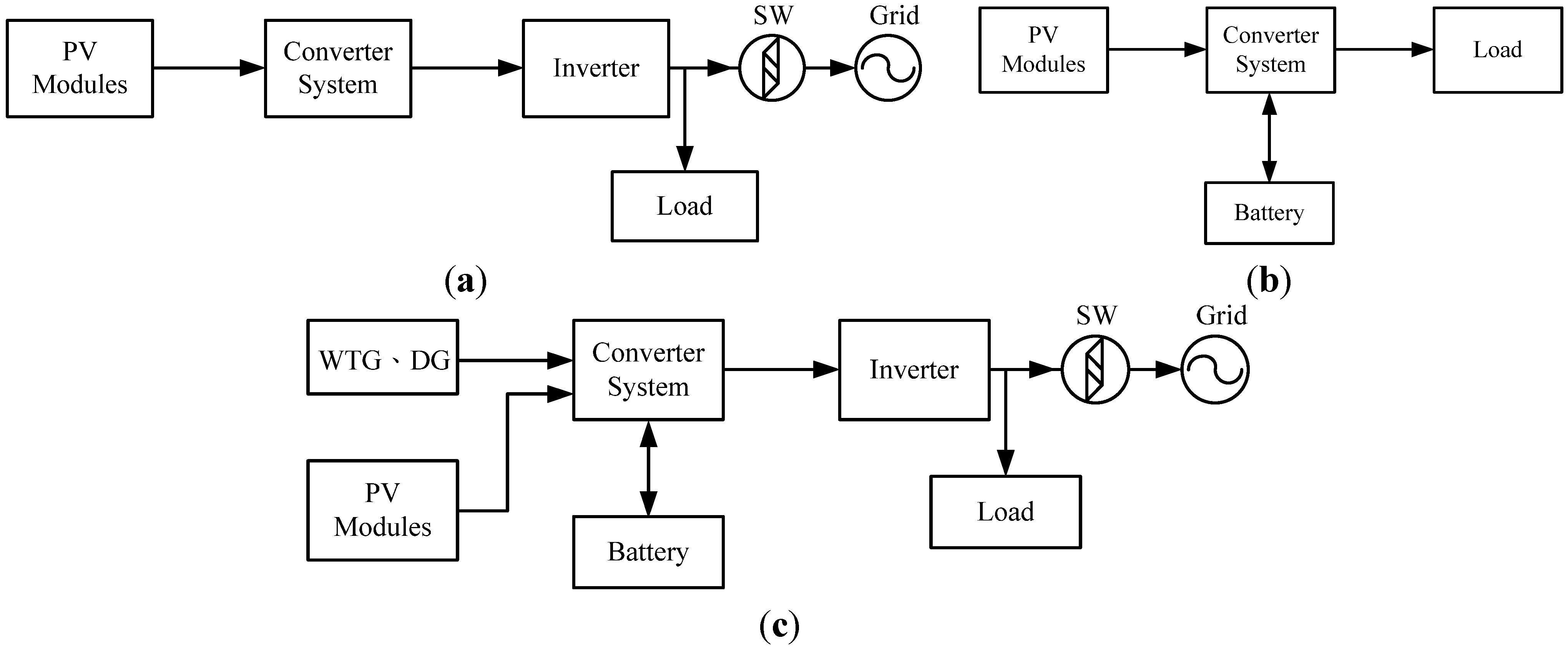
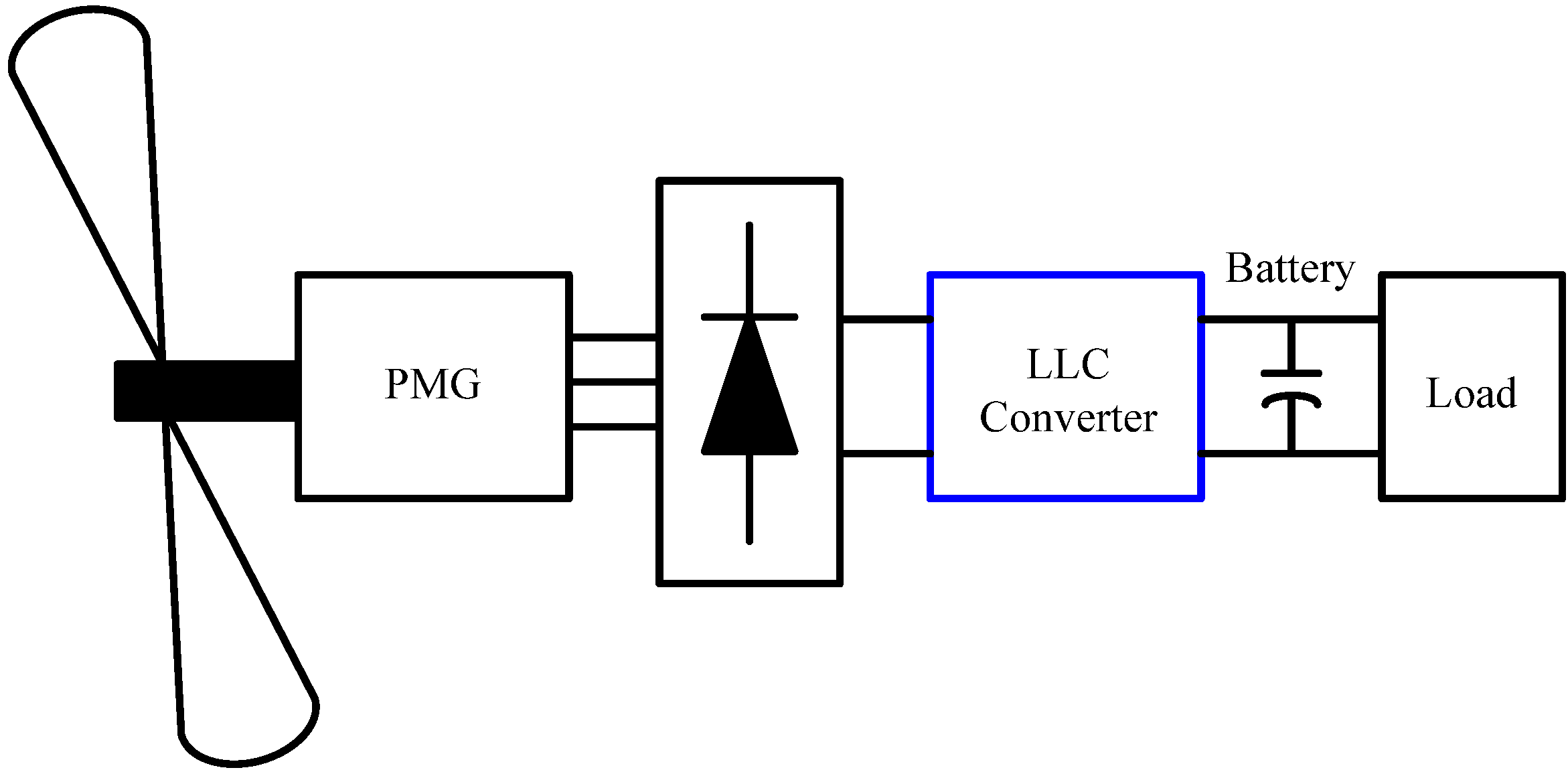
:1. Introduction


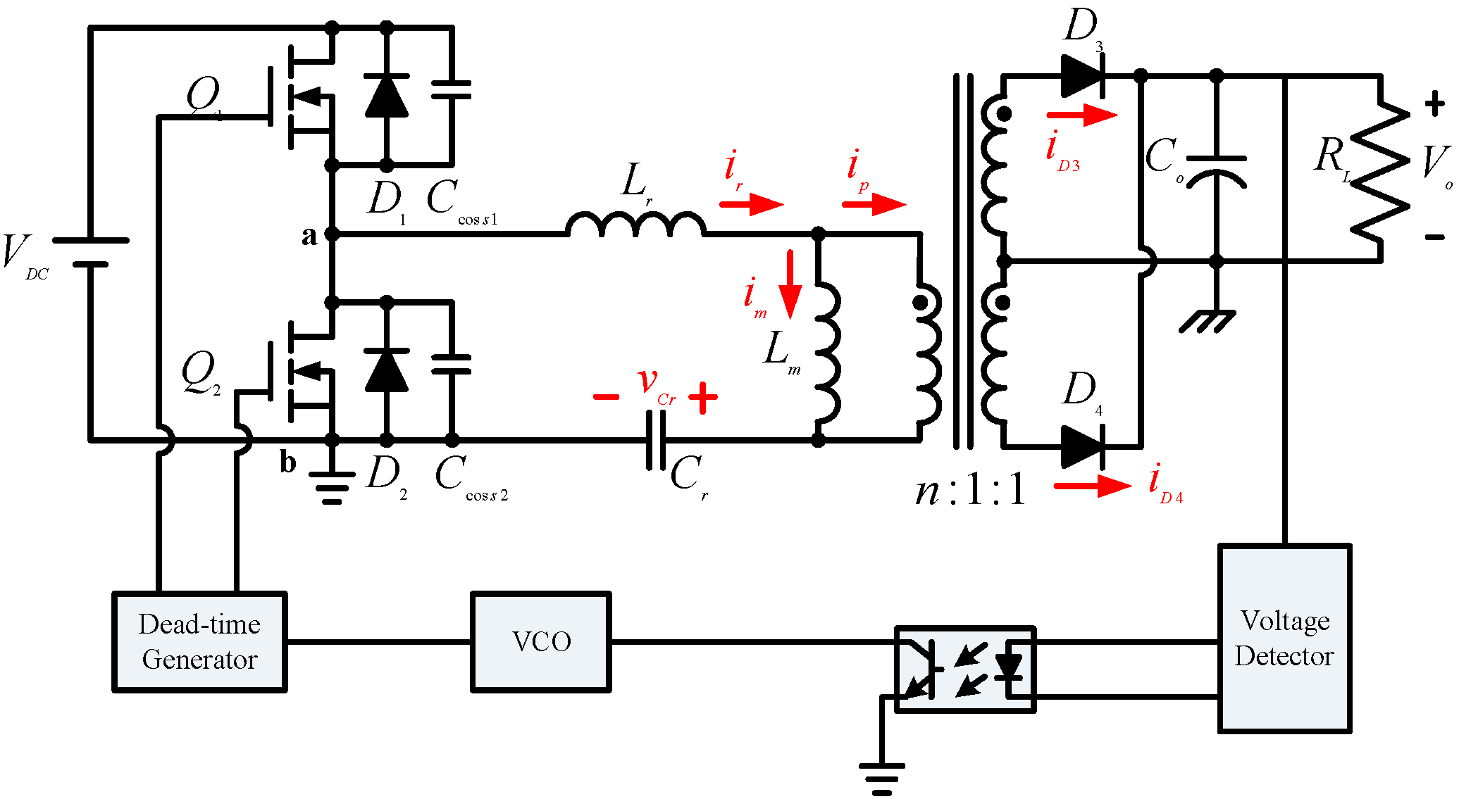
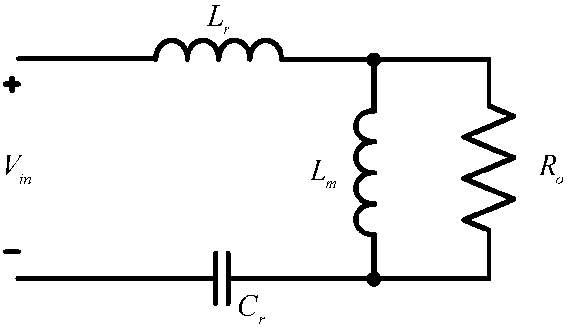
2. Conventional Schemes


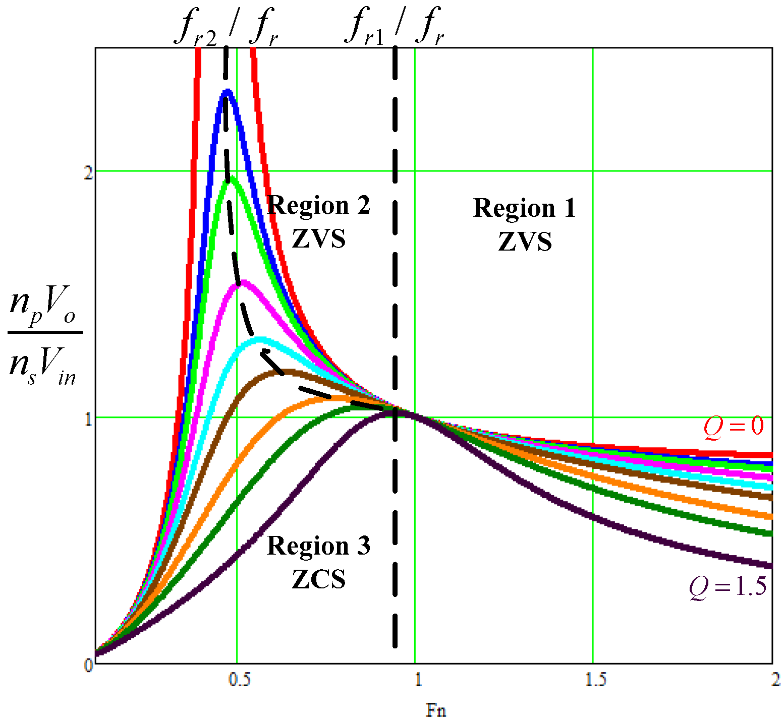
2.1. Operation of the Line Level Control Resonant Converter in Region 1 (Zero Voltage Switching)

2.2. Operation of the Line Level Control Resonant Converter in Region 2 (Zero Voltage Switching)


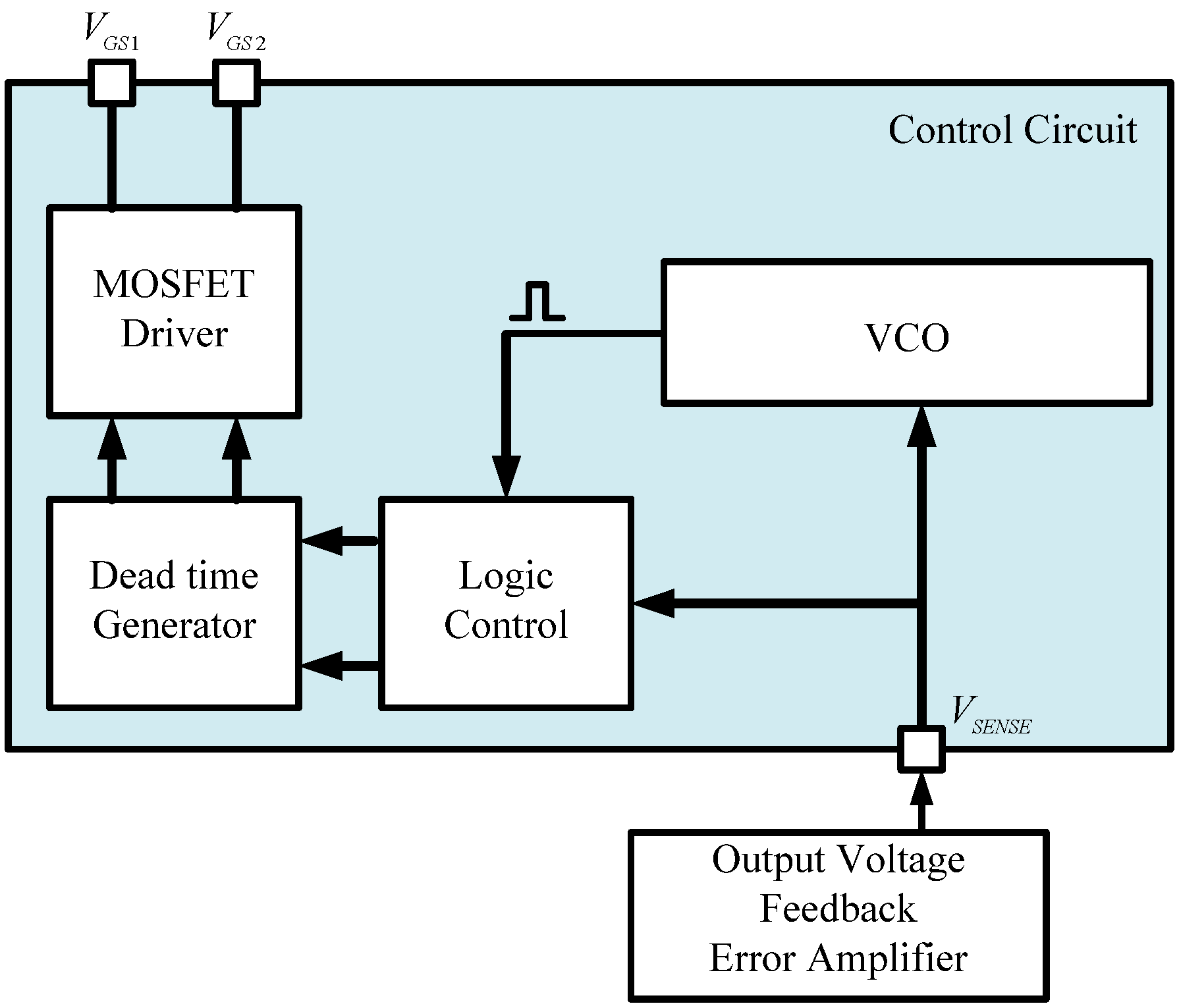
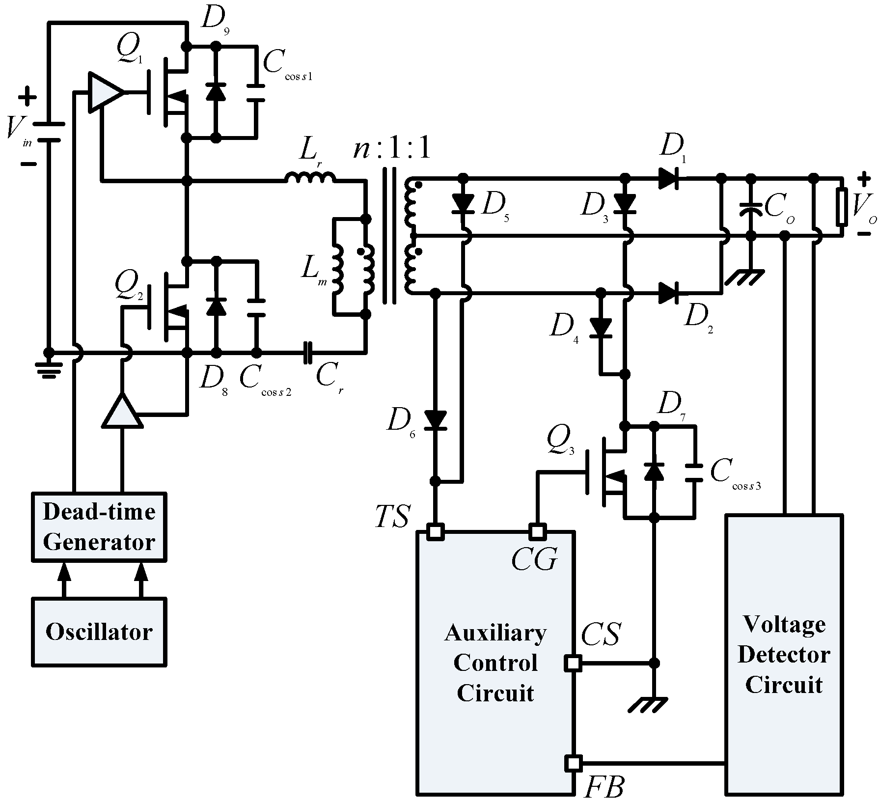
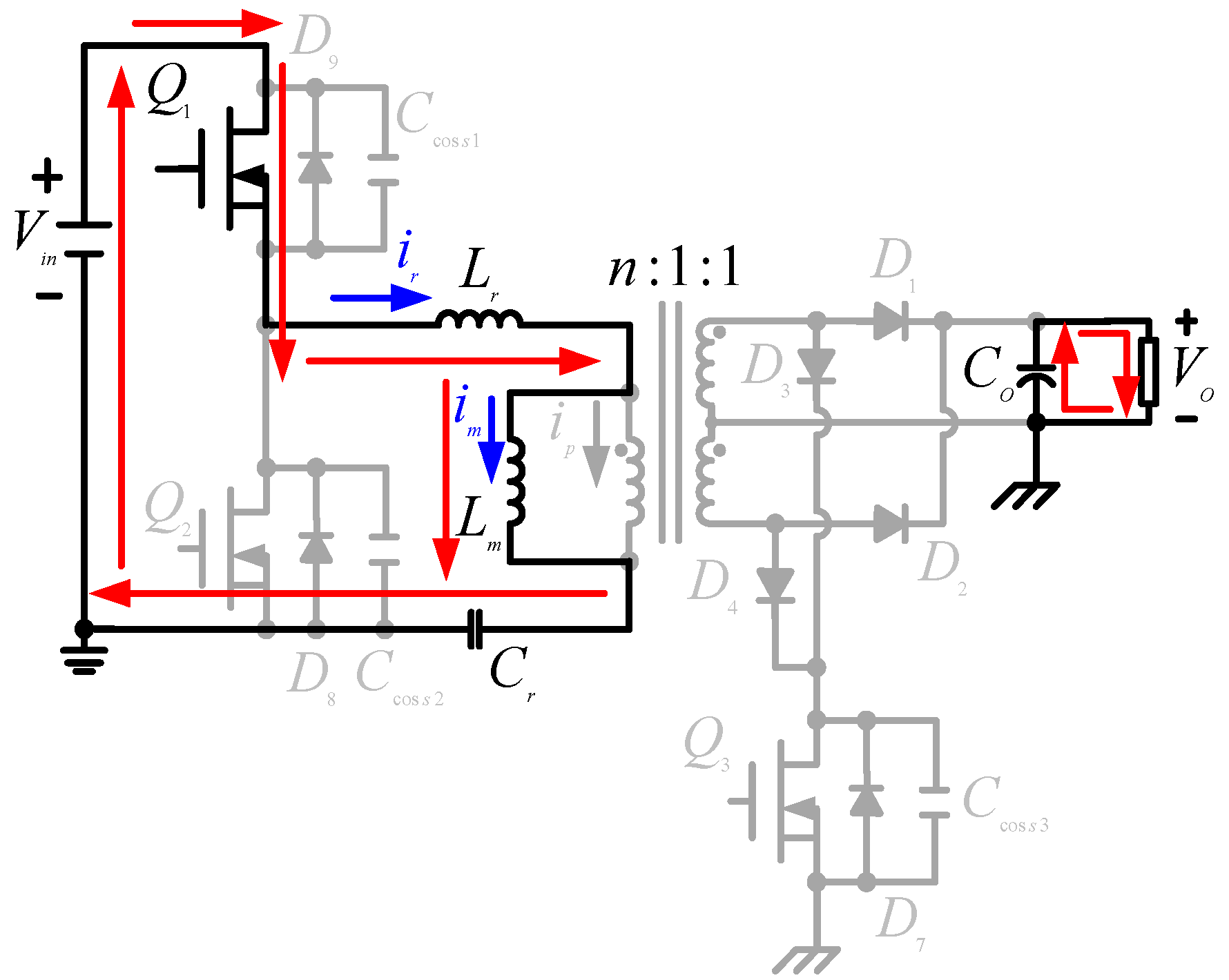
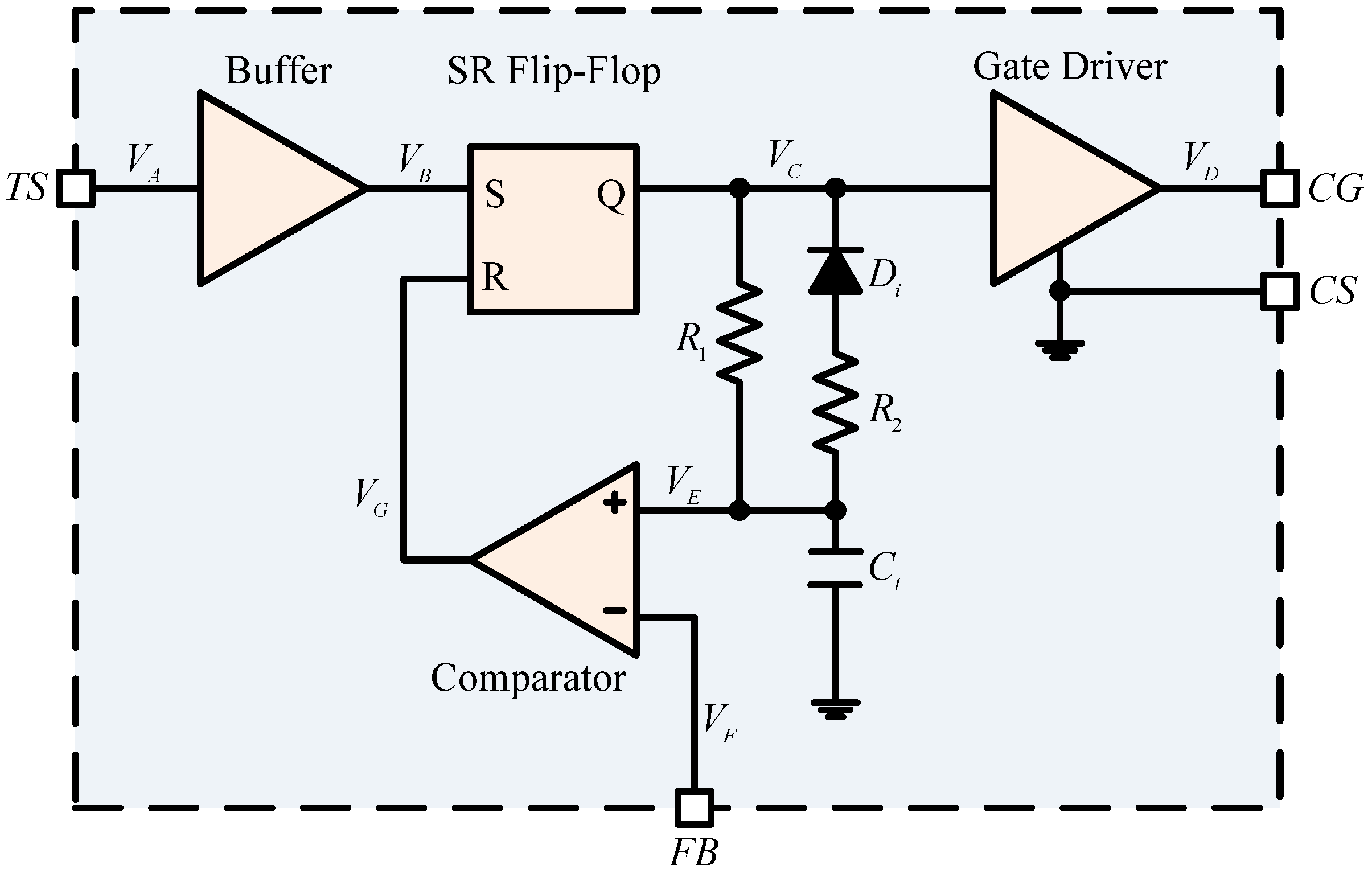
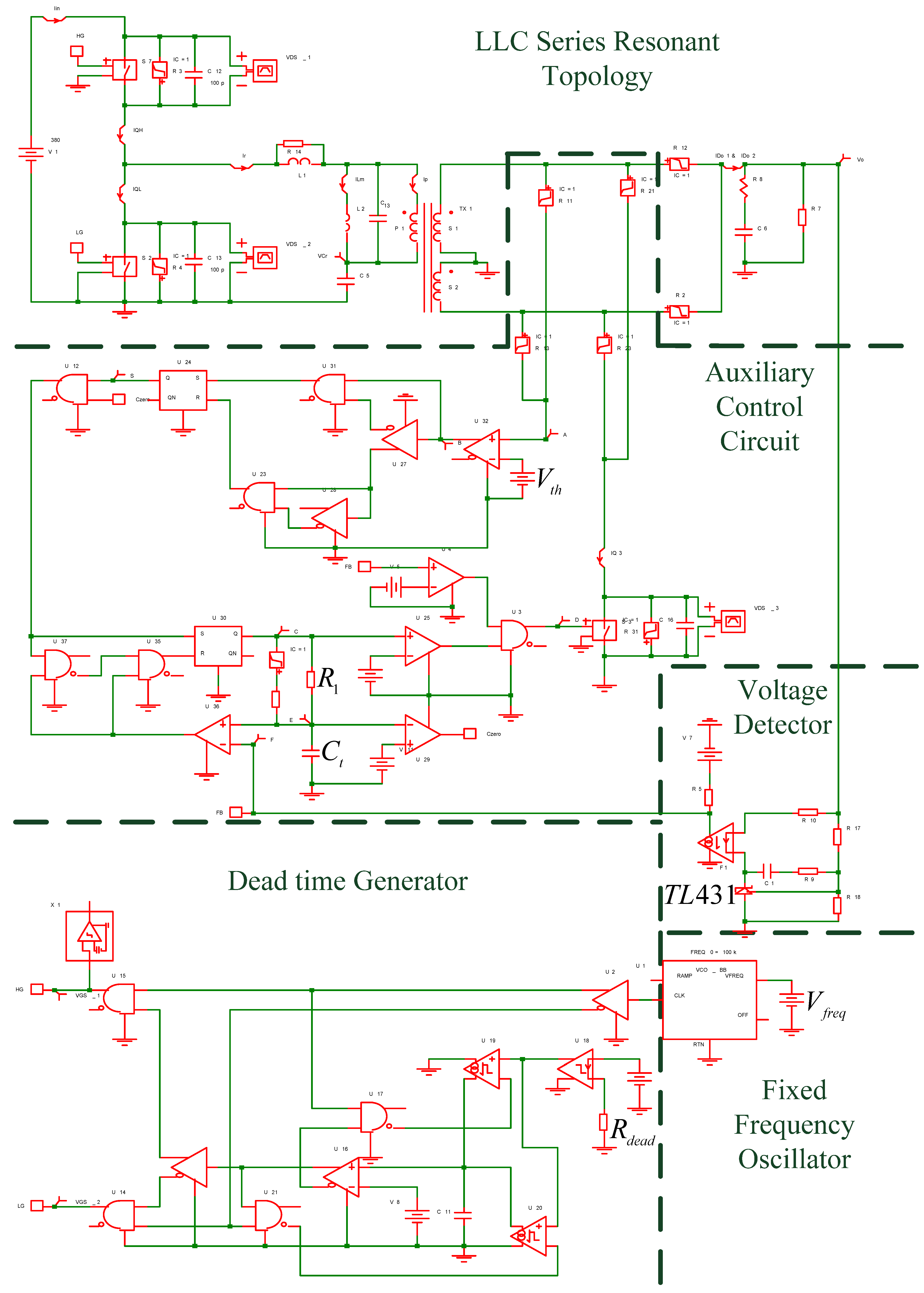
3. Novel Line Level Control Circuit


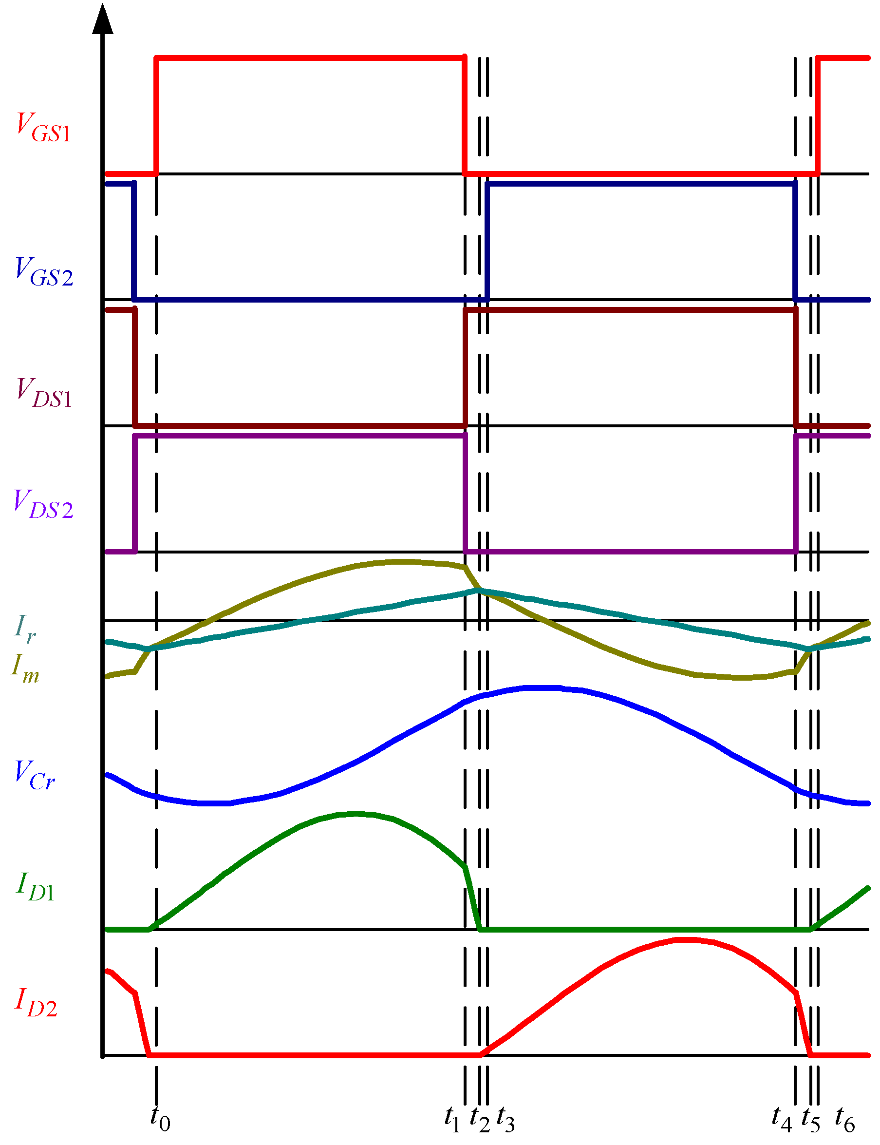
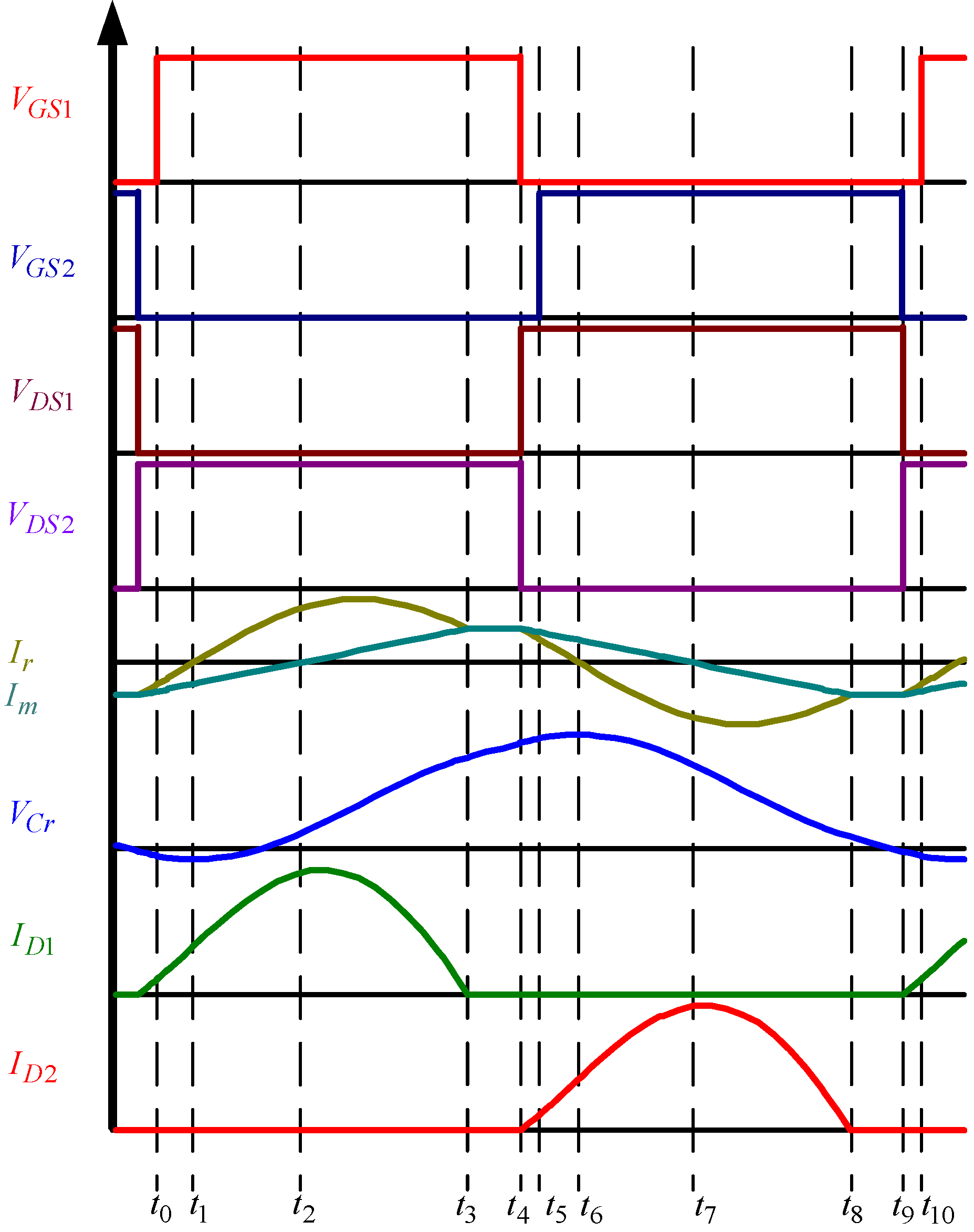
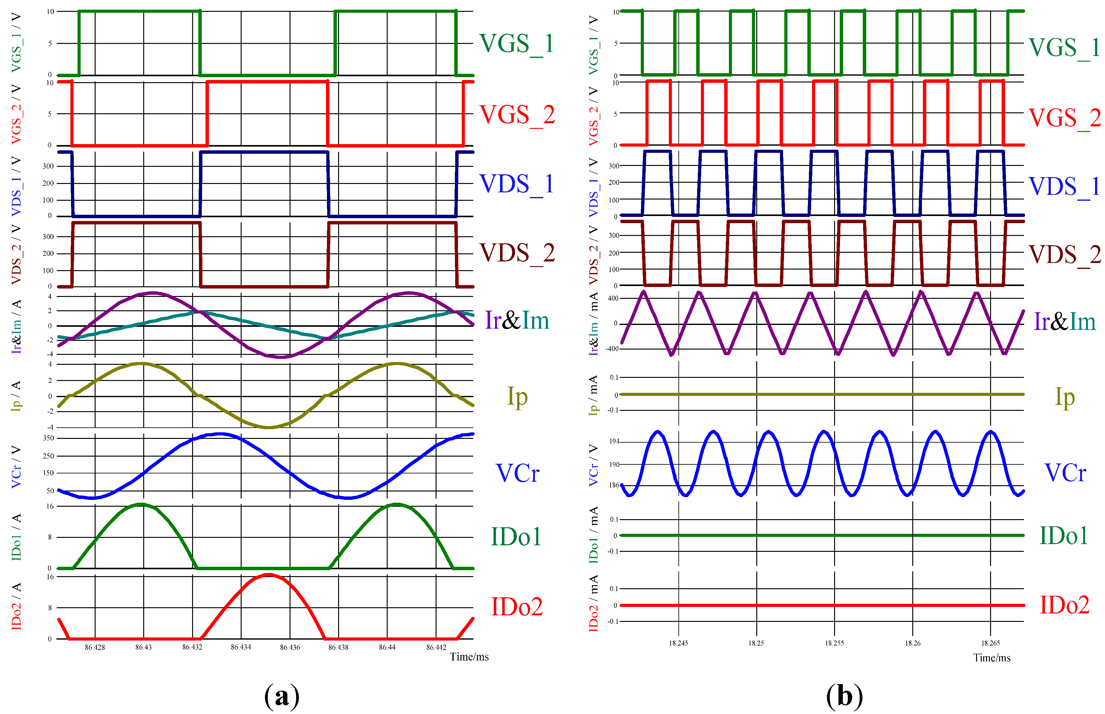
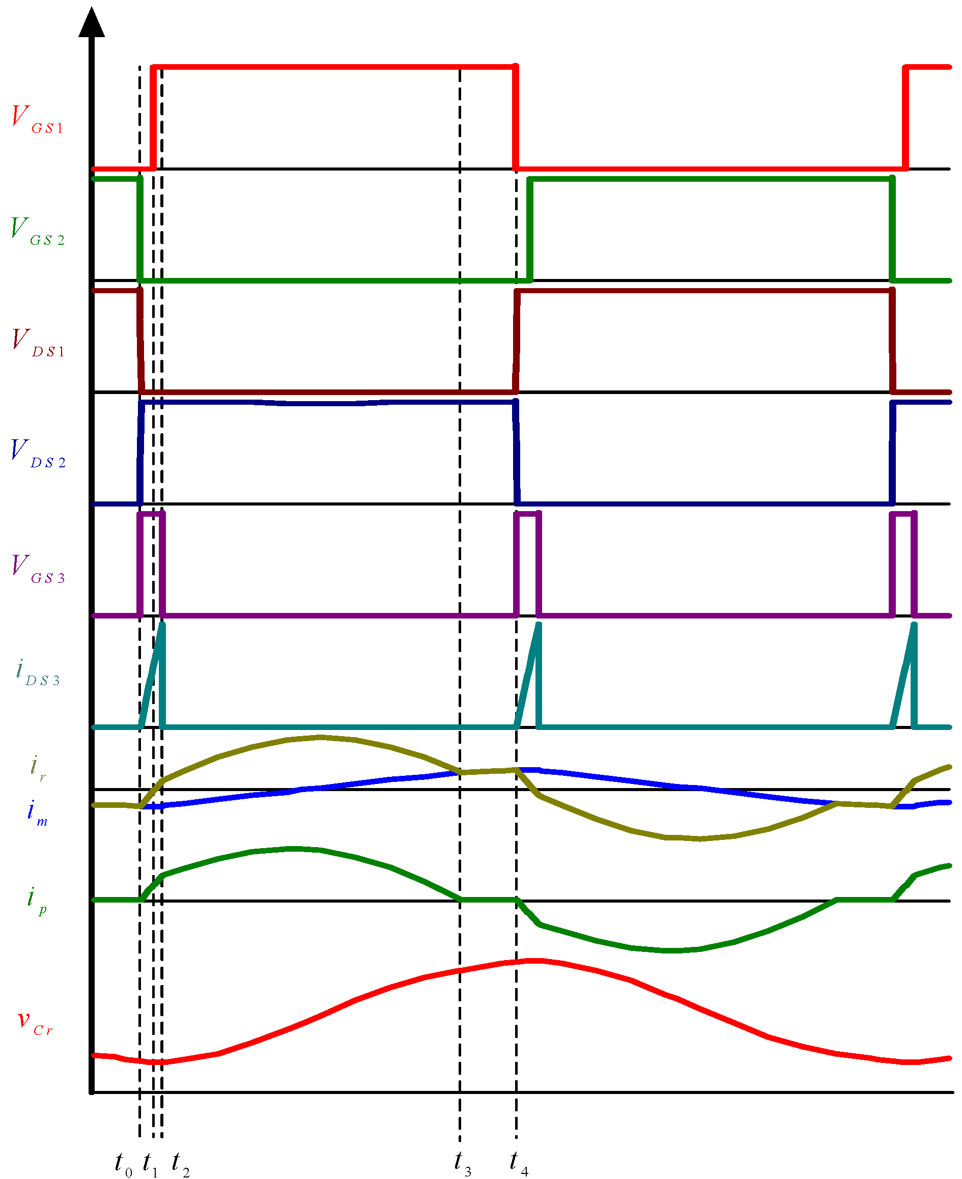
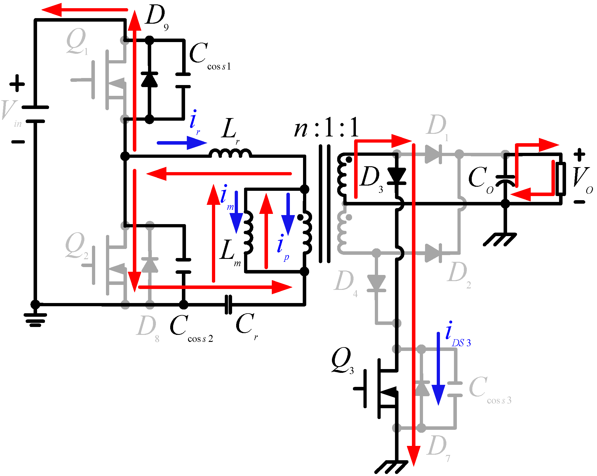
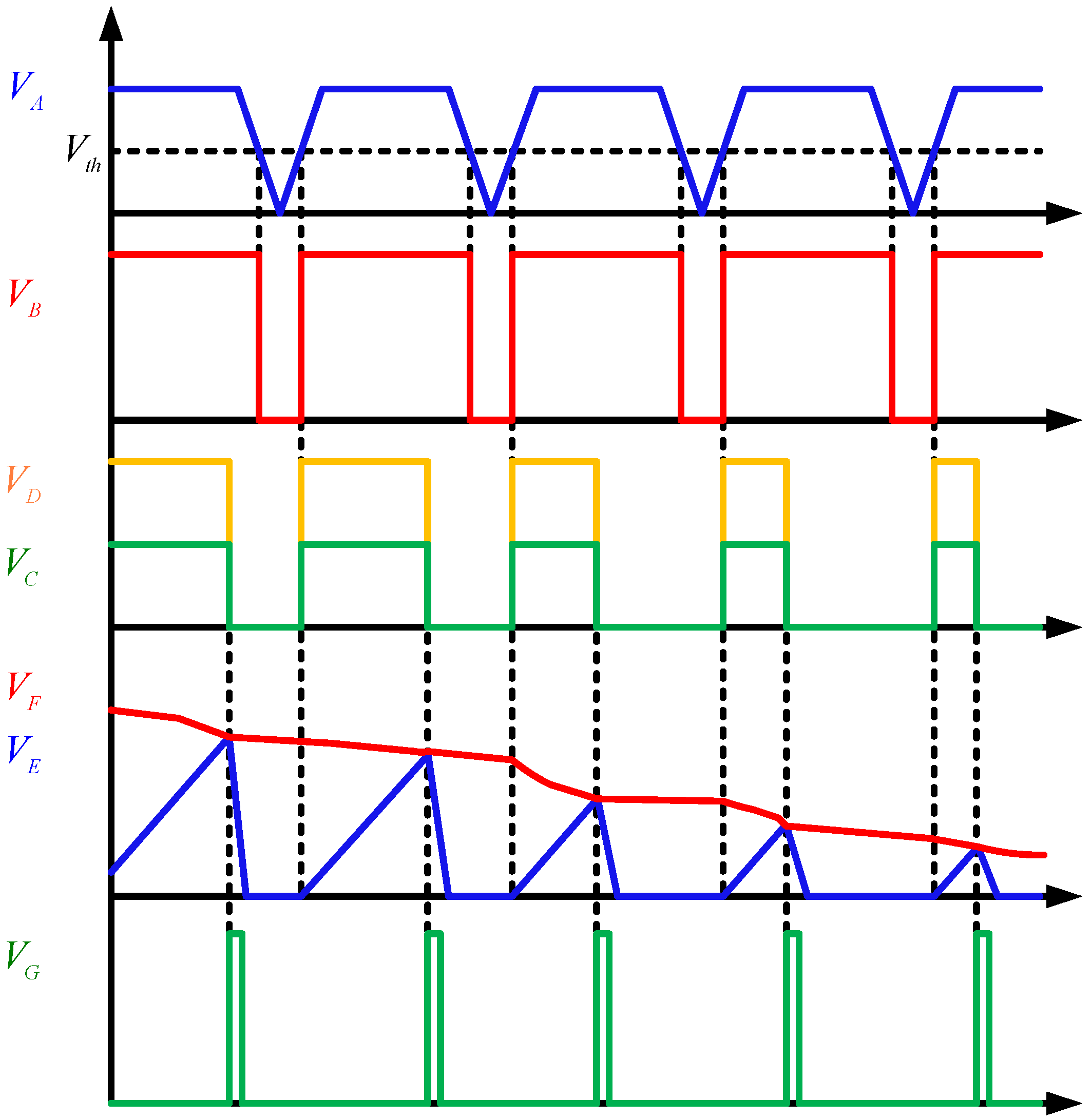
3.1. Working State 1 (t0 ≤ t ≤ t1)

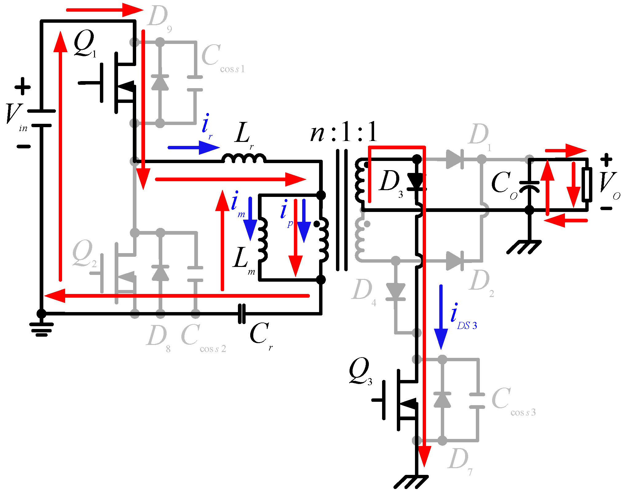
3.2. Working State 2 (t1 ≤ t ≤ t2)

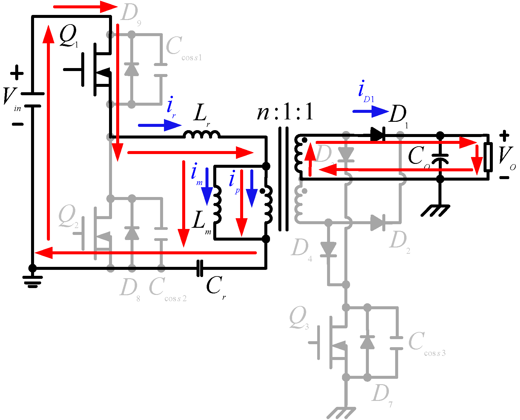
3.3. Working State 3 (t2 ≤ t ≤ t3)

3.4. Working State 4 (t3 ≤ t ≤ t4)


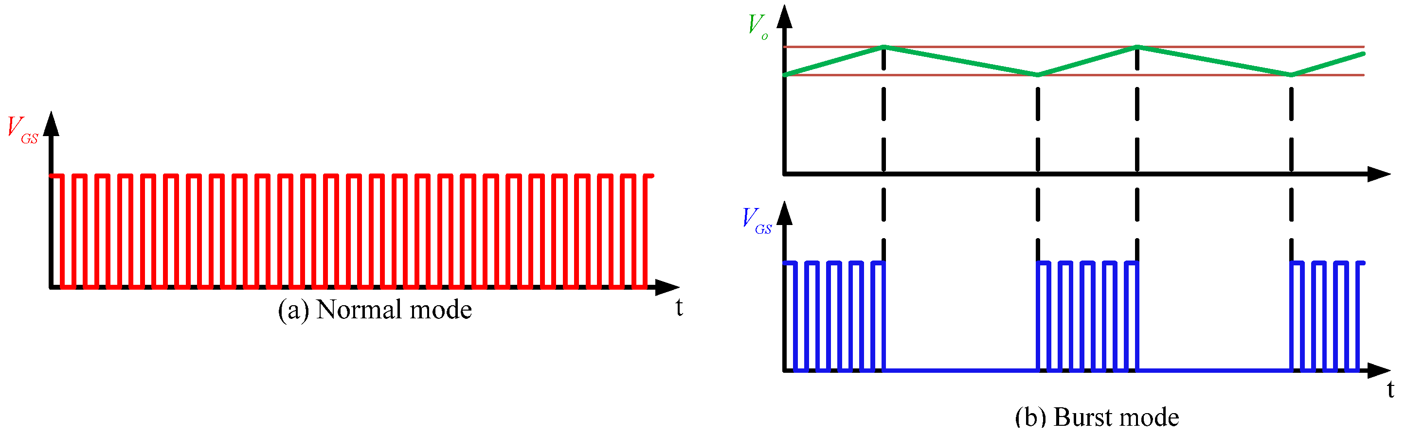
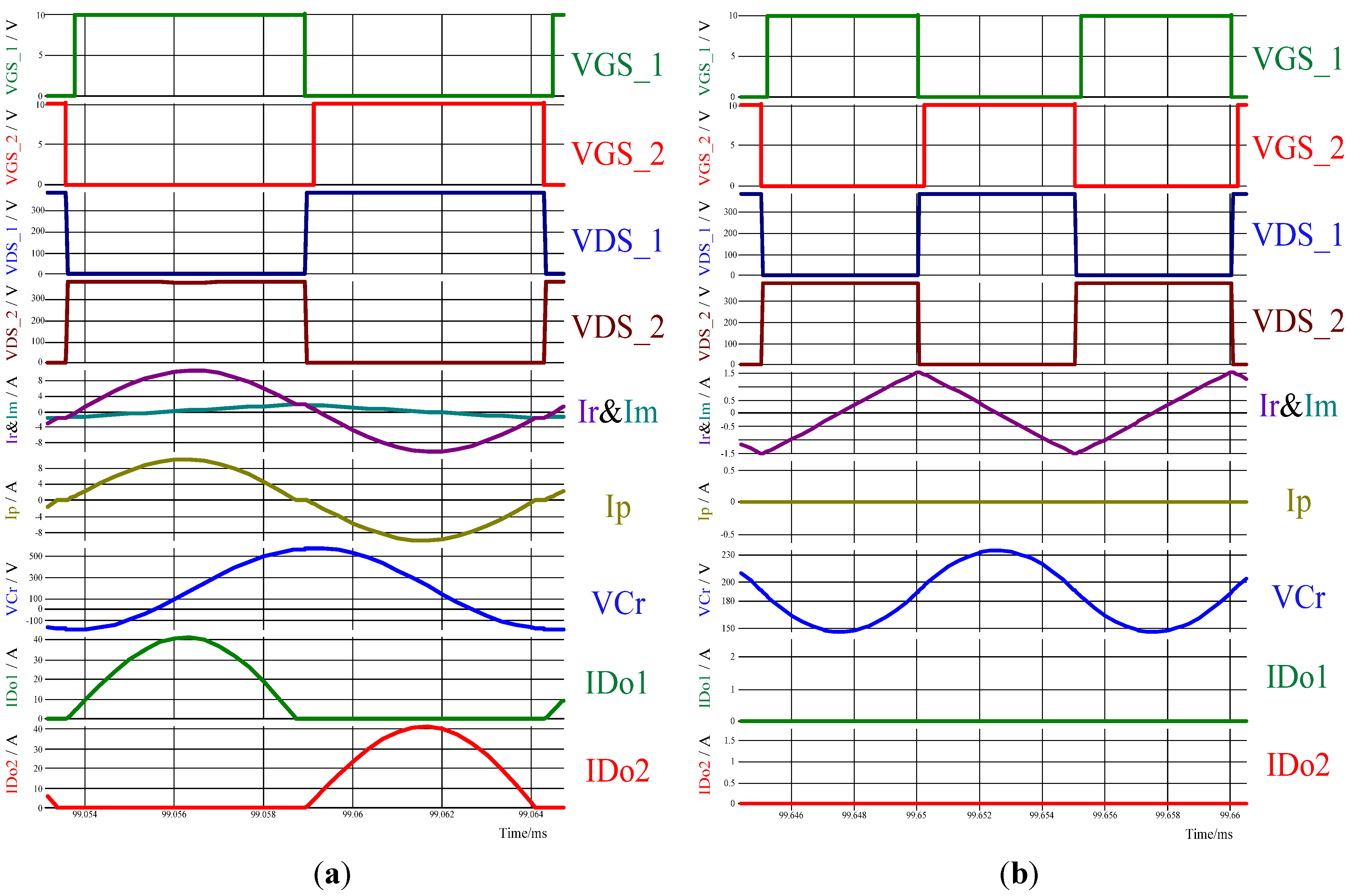
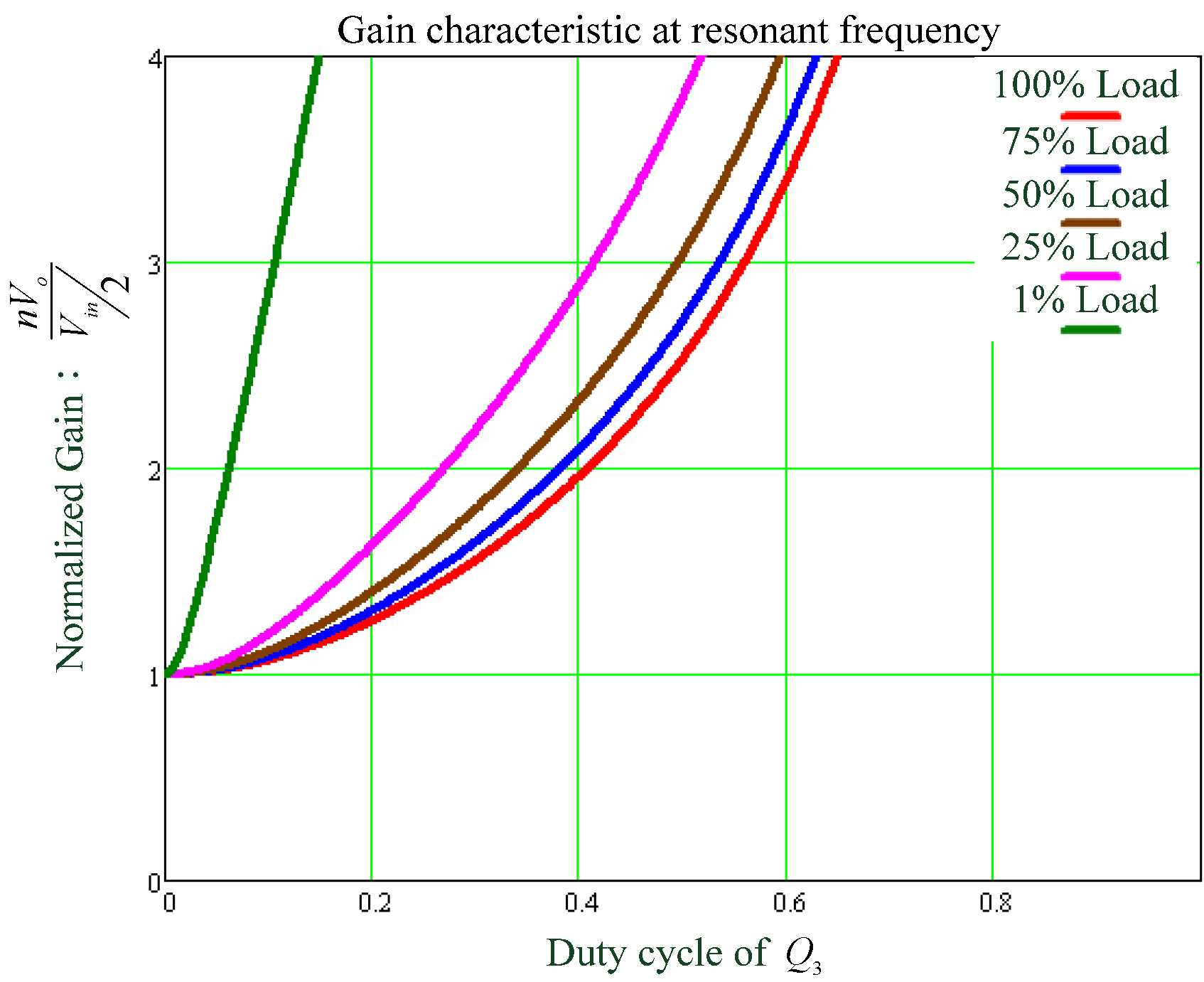
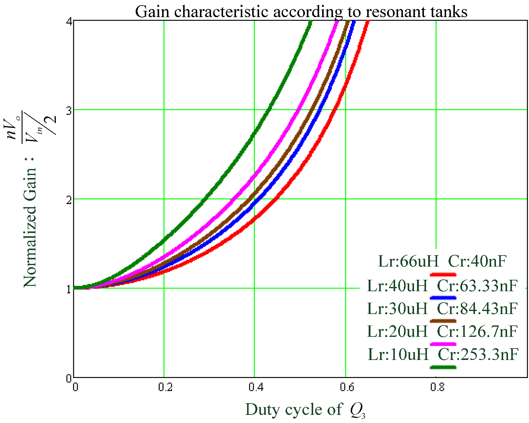
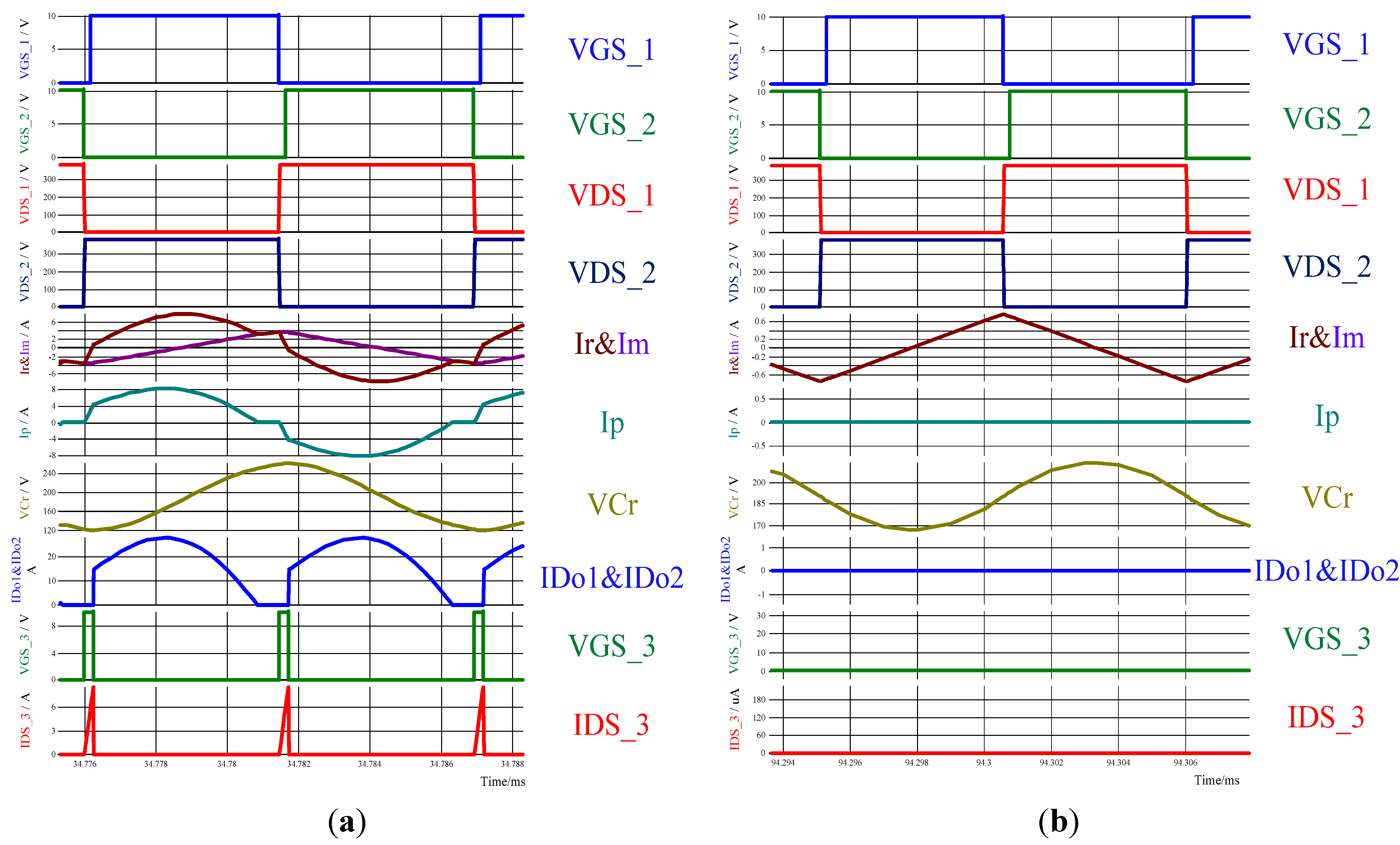
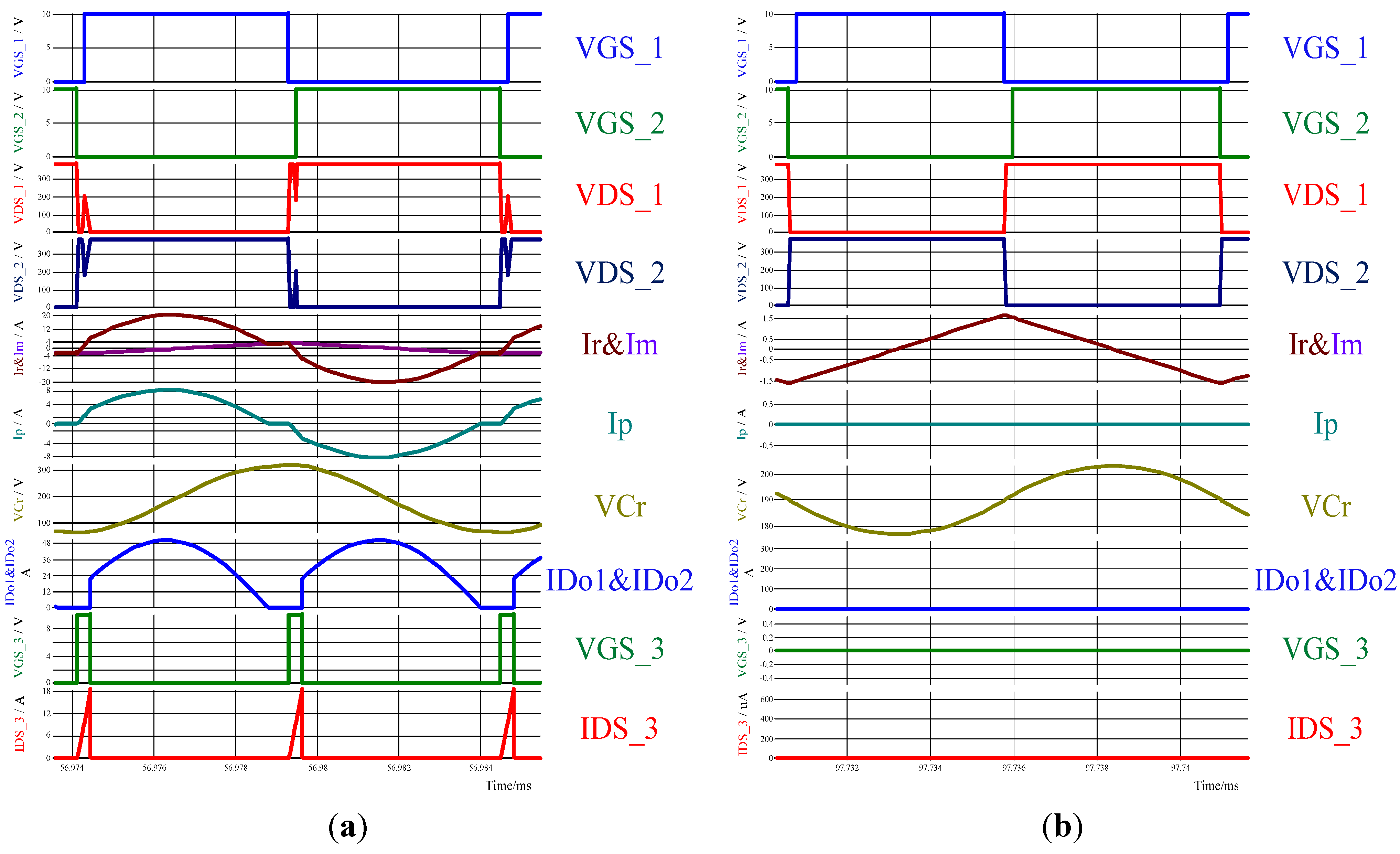
4. Simulation Results and Analysis
- (1)
- The simulated circuit and function block diagram are built and behaves following proposed operation principles truly, as shown in Figure 22.


| 480 W/48 V@100% load | fSW | Iin_peak | fQ3 | |
|---|---|---|---|---|
| Conventional LLC | 98.89 kHz | 4.521 A | N/A | |
| Proposed LLC | 99 kHz | 6.827 A | 198 kHz | |
| 480 W/48 V@0% load | fSW | Iin_peak | Iin_rms | fQ3 |
| Conventional LLC | 285.15 kHz | 0.688 A | 0.327 A | N/A |
| Proposed LLC | 95 kHz | 1.018 A | 0.486 A | 0 Hz |
| 1200 W/48 V@100% load | fSW | Iin_peak | fQ3 | |
| Conventional LLC | 96.52 kHz | 12.016 A | N/A | |
| Proposed LLC | 96 kHz | 23.791 A | 186 kHz | |
| 1200 W/48 V@0% load | fSW | Iin_peak | Iin_rms | fQ3 |
| Conventional LLC | 258.47 kHz | 1.810 A | 0.824 A | N/A |
| Proposed LLC | 96 kHz | 2.360 A | 1.076 A | 0 Hz |


| Specification | Type | Conventional LLC | Novel LLC | |
|---|---|---|---|---|
| 480 W/48 V | MOS-FDP12N50 | Rpri 0.2 Ω | 2.0305 W | 1.1846 W |
| 1200 W/48 V | MOS-FDA28N50 | Rpri 0.08 Ω | 10.9608 W | 5.4568 W |
5. Conclusions
- (1)
- Systems with proposed control schemes achieve optimal standby power consumptions.
- (2)
- Even though the magnetizing inductance remains unchanged, the resonant inductance is permitted with a relatively small design, bringing advantages such as smaller volumes of magnetic components and improving power density.
- (3)
- This system can also enhance current gain and operate in a wide input range. The hold-up time increases, which reduces capacitance size and improves power density; additionally, operating range of wind generators gets improved.
- (4)
- The control loop at system input and output side is independent, and therefore, isolation between control circuits is naturally accomplished.
Acknowledgments
Author Contributions
Conflicts of Interest
References
- Giraud, F.; Salameh, Z.M. Steady-state performance of a grid-connected rooftop hybrid wind-photovoltaic power system with battery storage. IEEE Trans. Energy Convers. 2001, 16, 1–7. [Google Scholar] [CrossRef]
- Nehrir, M.H.; LaMeres, B.J.; Venkataramanan, G.; Gerez, V.; Alvarado, L.A. Performance Evaluation of Stand-Alone Wind/Photovoltaic Genera System. In Proceedings of the IEEE Power Engineering Society Summer Meeting, Edmonton, AB, Canada, 18–22 July 1999; Volume 1. pp. 555–559.
- Park, S.J.; Kang, B.B.; Yoon, J.P.; Cha, I.S.; Lim, J.Y. A Study on the Stand-Alone Operating or Photovoltaic/Wind Power Hybrid Generation System. In Proceedings of the IEEE 35th Annual Power Electronics Specialists Conference, PESC 04, Aachen, Germany, 20–25 June 2004; Volume 3, pp. 2095–2099.
- Dou, X.; Quan, X.; Wu, Z.; Hu, M.; Sun, J.; Yang, K.; Xu, M. Improved control strategy for microgrid ultracapacitor energy storage systems. Energies 2014, 7, 8095–8115. [Google Scholar] [CrossRef]
- Drouilhet, S.; Muljadi, E.; Holz, R.; Gevorgian, V. Optimizing Small Wind Turbine Performance in Battery Charging Applications; NREL/TP-441–7808; National Renewable Energy Laboratory (NREL): Golden, CO, USA, 1995. [Google Scholar]
- Lee, F.C.; Barbosa, P.; Xu, P.; Zhang, J.; Yang, B.; Canales, F. Topologies and design considerations for distributed power system applications. Proc. IEEE 2001, 89, 939–950. [Google Scholar] [CrossRef]
- Krishna, R.A.; Dutt, A.A. Resonant Converter with Renewable Energy Source for Low Voltage Application. In Proceedings of the 2011 International Conference on Signal Processing, Communication, Computing and Networking Technologies (ICSCCN), Thuckafay, India, 21–22 July 2011; pp. 383–388.
- Yang, B.; Lee, F.C.; Zhang, A.J.; Huang, G.S. LLC Resonant Converter for Front End DC/DC Conversion. In Proceedings of the Seventeenth Annual IEEE Applied Power Electronics Conference and Exposition, APEC 2002, Dallas, TX, USA, 10–14 March 2002; Volume 2, pp. 1108–1112.
- Yang, B. Topology Investigation for Front End DC/DC Power Conversion for Distributed Power. Ph.D. Thesis, Virginia Tech, Blacksburg, VA, USA, 2003. [Google Scholar]
- Fang, Y.; Xu, D.; Zhang, Y.; Gao, F.; Zhu, L.; Chen, Y. Standby Mode Control Circuit Design of LLC Resonant Converter. In Proceedings of the IEEE Power Electronics Specialists Conference, PESC 2007, Orlando, FL, USA, 17–21 June 2007; pp. 726–730.
- Ye, Y.; Yan, C.; Zeng, J.; Ying, J. A Novel Light Load Solution for LLC Series Resonant Converter. In Proceedings of the 29th International Telecommunications Energy Conference, INTELEC 2007, Rome, Italy, 30 September–4 October 2007; pp. 61–65.
- Jung, J.-H.; Kwon, J.-G. Theoretical Analysis and Optimal Design of LLC Resonant Converter. In Proceedings of the 2007 European Conference on Power Electronics and Applications, Aalborg, Denmark, 2–5 September 2007; pp. 1–10.
- Cheng, C.A.; Chen, H.W.; Chang, E.C.; Yen, C.H.; Lin, K.J. Efficiency Study for a 150W LLC Resonant Converter. In Proceedings of the International Conference on Power Electronics and Drive Systems, PEDS 2009, Taipei, Taiwan, 2–5 November 2009; pp. 1261–1265.
- Kim, B.-C.; Park, K.-B.; Kim, C.-E.; Lee, B.-H.; Moon, G.-W. LLC resonant converter with adaptive link-voltage variation for a high-power-density adapter. IEEE Trans. Power Electron. 2010, 25, 2248–2252. [Google Scholar] [CrossRef]
© 2015 by the authors; licensee MDPI, Basel, Switzerland. This article is an open access article distributed under the terms and conditions of the Creative Commons Attribution license (http://creativecommons.org/licenses/by/4.0/).
Share and Cite
Kuo, M.-T.; Tsou, M.-C. Simulation of Standby Efficiency Improvement for a Line Level Control Resonant Converter Based on Solar Power Systems. Energies 2015, 8, 338-355. https://doi.org/10.3390/en8010338
Kuo M-T, Tsou M-C. Simulation of Standby Efficiency Improvement for a Line Level Control Resonant Converter Based on Solar Power Systems. Energies. 2015; 8(1):338-355. https://doi.org/10.3390/en8010338
Chicago/Turabian StyleKuo, Ming-Tse, and Ming-Chang Tsou. 2015. "Simulation of Standby Efficiency Improvement for a Line Level Control Resonant Converter Based on Solar Power Systems" Energies 8, no. 1: 338-355. https://doi.org/10.3390/en8010338