Article

Simple Design Scheme for a 300 kW Modular NPC Inverter Using Thermal RC Network Analysis

1
Electric Machines and Drives Research Center, Korea Electrotechnology Research Institute, Changwon-si 51543, Republic of Korea
2
School of Electrical Engineering, Pusan National University, Busan 46241, Republic of Korea
*
Authors to whom correspondence should be addressed.
Energies 2024, 17(2), 393; https://doi.org/10.3390/en17020393
Submission received: 20 November 2023 / Revised: 3 January 2024 / Accepted: 5 January 2024 / Published: 12 January 2024
(This article belongs to the Topic Power Converters)

Abstract

:
This paper proposes a simple design scheme for a modular NPC inverter using thermal RC network analysis. The proposed design process is an efficient and straightforward approach to designing the heatsink for a 300 kW modular neutral-point-clamped inverter. The heatsink design plays a crucial role in achieving high power density of a power converter because the weight and size of the heatsink are primarily influenced by its type. The structure and dimensions of the heatsink are mainly determined based on the generated heat by losses of the power semiconductor switches. In this paper, a thermal RC network model was established using parameters from the power switch module and was applied to the simulation of the power converter. The thermal losses of the power semiconductor switches were calculated via this process, and the heatsink was designed according to the calculated thermal losses. The proposed design scheme was analyzed and compared with the thermal fluid dynamic model. To validate the feasibility of the proposed design process, The simulation results were compared with experimental results.

1. Introduction

Recently, electric propulsion systems have replaced mechanical propulsion systems in ships, thereby improving fuel efficiency, reducing emissions, and facilitating the adjustment of ship space [1]. These electric propulsion systems consist of an electric motor, a power converter, and a reducer that is differently used by the characteristic of a ship. Since a ship requires a high-power system, power converters have been widely used by multi-level inverters, which have advantages such as high-power conversion and a reduction in harmonics despite a low switching frequency. Especially, neutral-point-clamped (NPC) inverters have been applied to many different ships because it has relatively simple configurations compared with other multi-level topologies. Moreover, if the NPC inverter consists of modular power stacks, it can easily utilize space and expand the power capacity [2,3,4]. The loss of the power semiconductor device can be defined as the sum of the conduction loss, which is expressed as the product of the current flowing through the device and the applied voltage, and the switching loss, which is expressed as the product of the current flowing through the switch and the voltage applied during the ON and OFF transition periods. In particular, the switching loss may vary depending on the physical shape of the connected portion of the circuit and the characteristics of the power semiconductor device, such as the switching frequency, which varies according to the control method and the PWM implementation method [5]. In the case of a 3-level NPC inverter, switching and conduction losses are relatively large because the number of switches require a greater number of switching devices compared with a 2-level inverter, whereas the breakdown voltage of the power semiconductor device is halved. A power semiconductor with a low voltage rating is beneficial in miniaturizing the filter size, which in turn can reduce ripples [6].
Generally, the volume and size of the power converter depend on the size of the heat sink considering the topology and basic specification. Moreover, the optimized design, considering the thermal characteristics of the heat sink, can increase the power density of the inverter. The heat sink of a power converter is designed based on the heat generated from losses of a power semiconductor device. Furthermore, a design scheme that reflects the loss and heat information, which is obtained using a circuit simulation analysis program, has been studied in [7,8]. Heat loss analysis, which considers topology, power, and the load of the inverter, can minimize the size of the inverter heat sink with. This analysis can reduce the required development cost and time. As mentioned earlier, the heat generated by the power semiconductor switch is represented by the switching and conduction losses. The foundation for electro-thermal analysis of power electronic systems can be formulated by coupling the thermal model and power loss model with temperature [9,10].
There are existing common methods for thermal analysis such as numerical methods, finite element analysis, and computational fluid dynamics. These analysis methods are solved using 1D, 2D, and 3D heat diffusion equations; however, it is difficult to analyze the switching and conduction losses occurring inside the semiconductor device directly. The estimation of the junction temperature or the overall temperature at several critical locations in the power module is linked to thermal design, thermal management, reliability, and life expectancy. Accordingly, a compact thermal model represented by a thermal RC network is widely used in [11,12,13,14,15,16].
Foster and Cauer’s methods are widely used for thermal RC networks. The Foster method does not thermally ground all capacitors except one in the RC network, whereas in a Cauer network, all capacitors are grounded. Although a non-grounded capacitor does not work as a physical device, it can be easily conducted to the mathematical model, whereas if a grounded capacitor works as a physical device, it is relatively difficult to interpret mathematically. A Foster network can be converted into the equivalent Cauer network, which means that the junction temperature of the Foster network can be analyzed as that of its equivalent Cauer network. The transient junction temperature in the modular inverter can therefore be predicted using the Foster or Cauer network, which can be easily expressed mathematically. The thermal RC network consists of values of the resistor and capacitor and is typically extracted by fitting the transient temperature response of the RC network to the actual temperature response curve, which is determined by the same step input of the power [17,18].
In this paper, the simple design process was proposed by RC network thermal analysis to obtain the heat dissipation of an NPC inverter module for an MW-class high-capacity inverter; the losses of the IGBT module were simply calculated by PLECS, which is an electrical circuit simulation tool, based on the datasheet of IGBT module. The IGBT thermal analysis was analyzed by using RC network thermal analysis. The optimal RC structure and RC value were used; moreover, these were reflected in the temperature saturation process. The proposed design process is an efficient and straightforward approach to designing the heatsink for a 300 kW modular neutral-point-clamped inverter. To verify the feasibility of the heat dissipation design process using circuit simulation, the heat sink design considering the heat loss was performed using the thermal RC network by PLECS. The results of this simulation were compared with the experimental results.
The remainder of this paper is organized as follows. Section 2 describes the 3-level NPC inverter, and Section 3 deals with the inverter heat dissipation design model. Section 4 analyzes the simulation and the experimental results. Finally, Section 5 presents the conclusions.

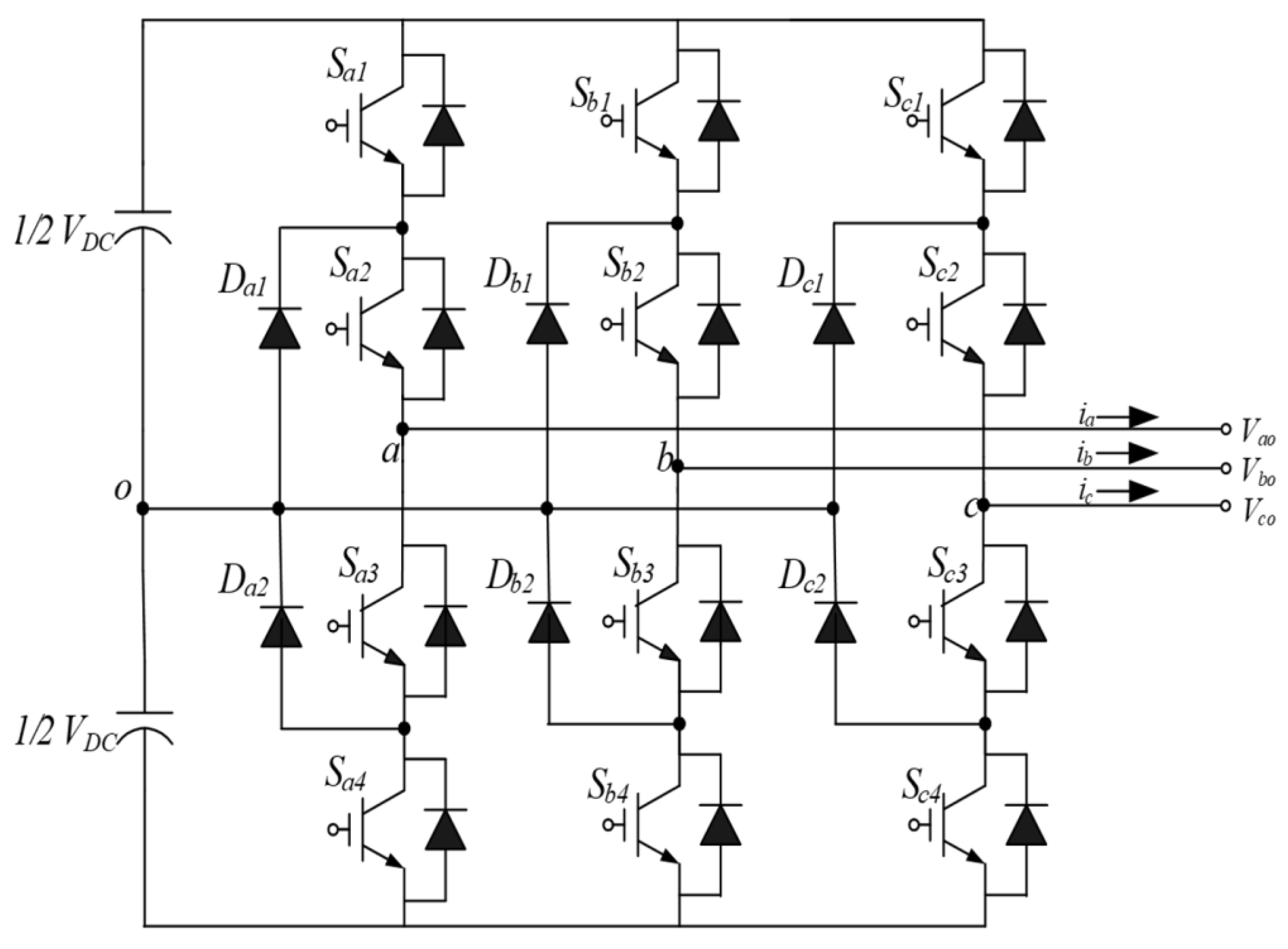
2. The 3-Level NPC Inverter

During the development of power conversion and motor systems, power conversion systems have recently been regarded as high-capacity and high-pressure systems [19]. Nevertheless, it is difficult to expect low THD and high efficiency in a high-capacity/high-voltage system using a conventional 2-level inverter. The current ripple can be reduced by increasing the switching frequency. Meanwhile, the DC voltage is kept sufficiently high; therefore, the breakdown voltage of the power semiconductor device is required. The 3-level NPC inverter structure was designed to solve this problem and has been recently used in high-voltage/high-capacity power converters [20]. The primary characteristic of the 3-level inverter is that a power semiconductor device with a lower voltage rating than the 2-level inverter can be used while maintaining an excellent ripple performance. Therefore, the filter size of the inverter can be reduced.
The NPC topology comprises four IGBTs in series with the inverter leg and a diode connected to the DC-Link neutral point, as depicted in Figure 1. This neutral point is connected to the output via a clamping diode in each phase. Moreover, the input voltage of the 3-level NPC inverter is a DC voltage, and the output pole voltage has the states VDC/2, 0, and −VDC/2.
Compared to a 2-level inverter whose output voltage fluctuates from VDC/2 to −VDC/2, the voltage fluctuation width is small; therefore, the output voltage harmonics can be reduced. As illustrated in Figure 2, when the switches Sx1 and Sx2 are ON and Sx3 and Sx4 are OFF, the switching state is ‘P’, and the output voltage is VDC/2. Conversely, when Sx1 and Sx2 are turned OFF, and Sx3 and Sx4 are turned ON, the ‘N’ switching state occurs, and the output voltage is −VDC/2. Finally, when Sx2 and Sx3 are ON and Sx1 and Sx4 are OFF, the switching state is ‘O’, and the output voltage is 0 V. Therefore, as the state of the switching element changes between ‘P-O-N,’ conduction and switching losses occur, leading to heat loss.

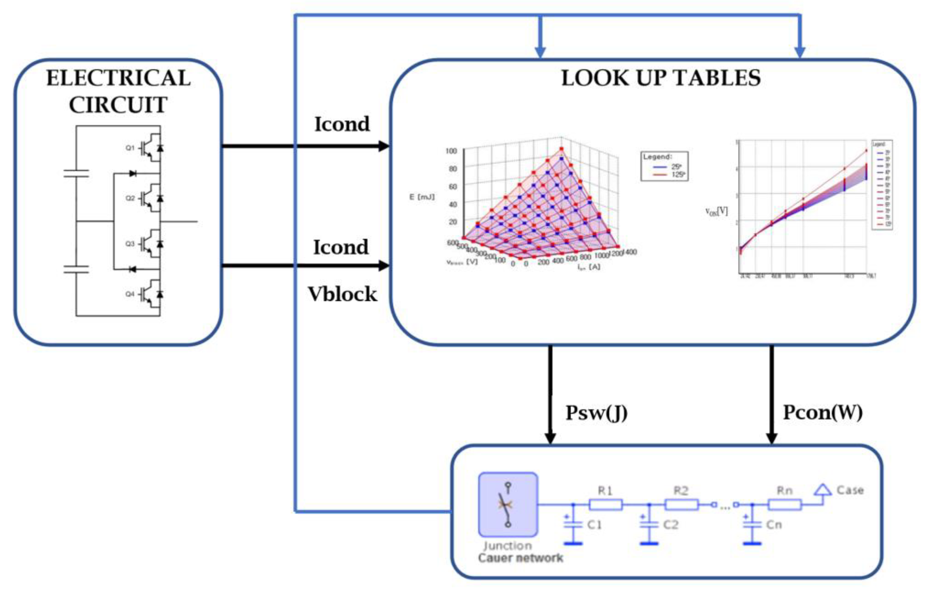
3. Inverter Heat Dissipation Design Model

The power semiconductor device is a vulnerable power electronic component, as shown in Figure 3, and the losses generated in the device directly affect the efficiency of its power conversion system. In addition, heat is generated due to the loss in the semiconductor device, which is the dominant reason behind system failure caused by stress source, as shown in Figure 4 [21,22,23]. Power semiconductor devices have different maximum junction temperatures, and during operation, they may exceed this temperature, resulting in damage or destruction. Therefore, when designing a power conversion system, conducting a relevant analysis is crucial.
The heat dissipation design of the inverter is based on the datasheet of the model. Moreover, the sum of the conduction and switching losses was first calculated to obtain the overall loss, as illustrated in Figure 5. Furthermore, each loss was converted into a thermal model using a simulation tool to track the device temperature in the next process.
The maximum value of each parameter was used to generate the maximum possible power loss at that instant. The temperature distribution tendency of each joint was evaluated based on the analyzed temperature. This was further used as the main parameter of the heat sink design.

3.1. Conduction Loss

Conduction loss occurs after the power semiconductor device becomes conductive, i.e., when it performs in the saturation region. It can be calculated using the following quantities: the current flowing through the power semiconductor device, the voltage applied to it, and the ON resistance, as represented by (1) [25].
P c o n d = 1 T V s w t i t d t = 1 T ( V O N + R O N i ( t ) ) i ( t ) d t = V O N I a v g + R O N ( i R M S ) 2
where Vsw is the collector–emitter saturation voltage, Von is the ON drop voltage, Ron is the ON resistance, Iavg is the average collector current, and iRMS is the RMS collector current. In this study, heat loss was calculated by making the device voltage an arbitrary function of device temperature during conduction using PLECS, and this function is displayed as a 2D look-up table in the range of 25–125 °C, as graphed in Figure 6. It is defined as the conduction loss tab of the Thermal Library Browser. The defined function can calculate the actual voltage drop at a given function value using linear interpolation.

3.2. Switching Loss

Switching loss occurs as a power loss because the power semiconductor device does not instantly switch from the ON state to the OFF state or vice versa, and its value is significantly greater than 0, as indicated by the yellow circles in Figure 7. It can be expressed as the relationship between energy loss, switching frequency, and voltage–current when the device is in the ON or OFF state, as expressed in (2).
P O N , O F F = E O N , O F F × f s w = V O N , O F F V t e s t × I O N , O F F I t e s t × E O N , O F F × f s w
where EON,OFF is turned ON or OFF energy loss, fsw is the switching frequency, VON,OFF is the switch input voltage, ION,OFF is the switch input current, and Vtest is the test input voltage on the datasheet. In this study, the switching loss was represented by a 3D look-up table plotted in Figure 8. Each value of the switching energy depends on the current flowing through the device, the temperature, and the blocking voltage. Moreover, the given value calculates the actual loss using linear interpolation and the conduction loss [25].

3.3. Heat Sink Design

The heat sink absorbs the heat loss of the device, and the core element of the heat loss calculation is based on the conduction and switching losses, leading to heat sink design. The heat transfer is the sum of the thermal resistance and thermal capacitance, as depicted in Figure 9a. This transfer process from the heat sink to the air can be modeled using the thermal impedance, which is based on the equivalence between the electrical and thermal variables, as provided in Table 1 [26].
The total loss generated by the switch is calculated using the relationship between the thermal characteristics, as expressed by (3) as follows [25]:
T j ° C = P L o s s W × R t h W + T A ° C R t h = R t h ( j c ) + R t h ( c h ) + R t h ( h a )
where Tj is junction temperature, PLoss is switch loss power, Rth is the total thermal resistance, Rth(jc) is the thermal resistance provided by the junction to the case, Rth(ch) is the thermal resistance provided by the case to the heat sink, Rth(ha) is the thermal resistance of the heat sink to the ambient temperature, and TA is the ambient temperature.
In this study, using the Cauer model, the system heat transfer function of each RC element is considered as depicted in Figure 9b, and the resultant step response of the thermal impedance can be expressed as follows (4) [27]:
Z t h e r m a l _ t r a n s f e r s = 1 s × C t h _ 1 + 1 R t h _ 1 + 1 s × C t h _ 2 + + 1 R t h _ n
where Zthermal_transfer is the thermal transfer function of the Cauer network, and Cth and Rth are the thermal capacitance and resistance, respectively.
Figure 10 presents the loss model of the PLECS simulation. This loss calculation method incorporates the ideal switch simulation concept combined with measured loss data provided in a lookup table format. The simulation of switch losses is conducted as follows:
  • The values of current (I) and voltage (V) applied to the switch are provided to look up the table after the switching event;
  • The calculated losses are added to the thermal circuit;
  • Temperature is fed back to look up the table for the next event;
  • Losses are calculated as functions of current, voltage, and temperature during switching;
  • The loss calculation is based on interpolation.
In this paper, the approach involves utilizing the switch loss data obtained via PLECS simulation to inform the design of a heat sink using computational fluid dynamics (CFD). The data obtained via simulation comprise both power loss and heat loss of the switch, providing insights into the thermal characteristics. By integrating these data into CFD, it becomes possible to precisely analyze the thermal behavior of the heat sink and design an optimal heat sink.
CFD is a powerful tool used for predicting fluid dynamics and heat transfer, allowing for the calculation of real-world thermal and flow characteristics. It enables the consideration of geometric structure, surface properties, and cooling flow paths in the optimal heat design. Furthermore, CFD allows for the simulation of heat transfer characteristics in real environmental conditions, accounting for the impact of airflow around the heat sink and its exposure to the surrounding environment. This approach facilitates the validation of heat sink design effectiveness by comparing experimental data with simulation results obtained via CFD. This methodology is expected to contribute to the effective design of a heat sink, taking into consideration thermal efficiency and system stability.

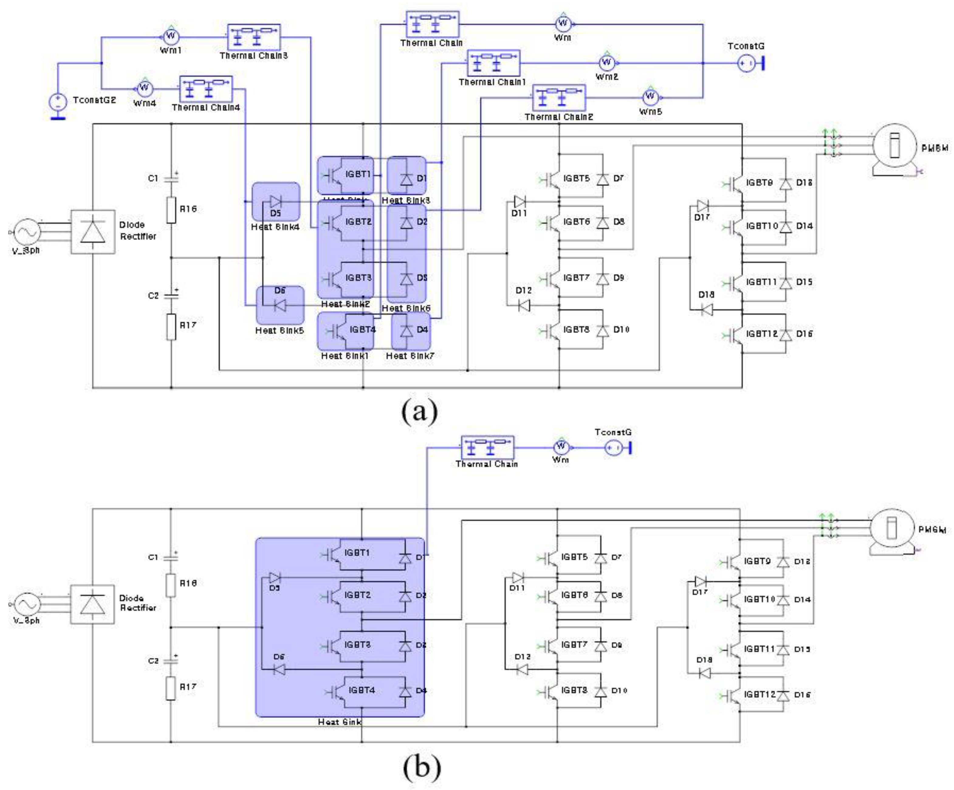
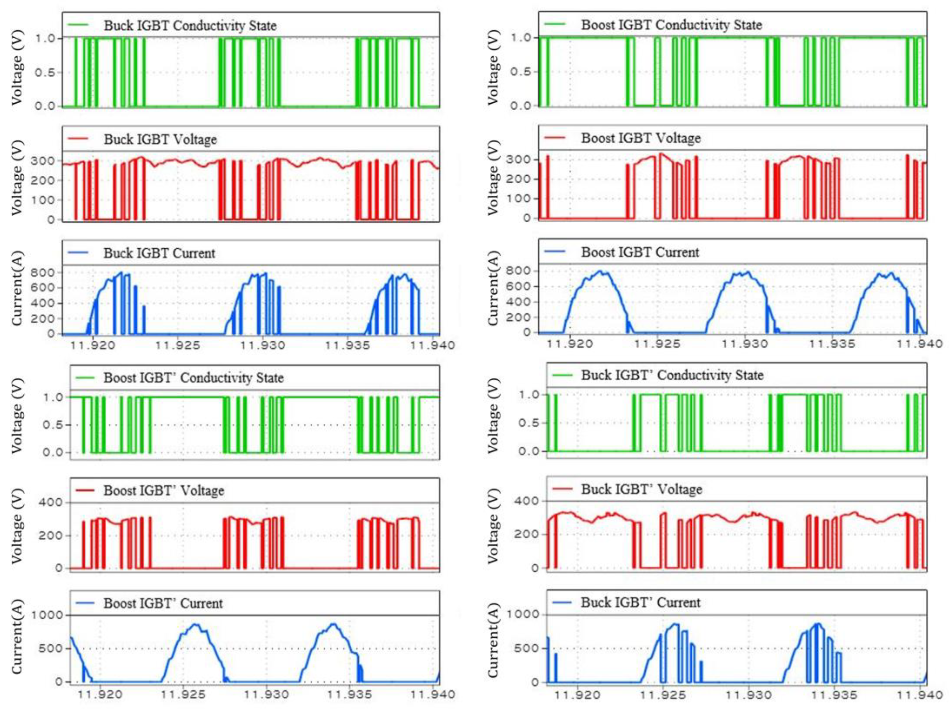
4. Simulation and Experiment Results

The heat loss analysis of the proposed 300 kW modular 3-level NPC inverter for the heat dissipation design was simulated by PLECS and is illustrated in Figure 11. The module used was Vincotech70-W424. It consists of the Buck IGBT, diode, Boost IGBT, diode, and Clamp diode, as shown in Figure 12. Each thermal resistance and capacitance are different. The modules and overall simulation parameters are detailed in Table 2 and Table 3. As shown in Table 3, since each heat impedance value is different for each heat sink, if all elements are simulated by using the shared heat sink as shown in Figure 11b, the impedance of each element cannot be reflected in the heat sink and only one common impedance is simulated. Therefore, it must be simulated by using the impedance of each element with a separated heat sink, as shown in Figure 11a.
Switching loss, conduction loss, and thermal impedance data parameters using a thermal editor were input to the IGBT element and the clamping diode, and the resultant values were derived via the set air temperature (25 °C) and heat sink. The thermal impedance values in the datasheet are the Foster network values, which, as mentioned earlier, can be mathematically converted to an equivalent Cauer network. This was executed automatically in the PLECS Thermal Editor to predict the transient junction temperature in the inverter. The average inverter loss value generated by the device was compared with the heat flow of the thermal circuit, and it was observed that the two values converged in the steady state, as plotted in Figure 13 and Figure 14. This means that thermal and electrical variables correspond with each other. Figure 13 is the result of using a separated heat sink, and Figure 14 is the result of using a shared heat sink.
As mentioned earlier, as a result of using the shared heat sink, the impedance of each element was the same. It leads to a larger impedance applied to a relatively small impedance. Hence, it causes more loss. The conduction loss observed in Boost IGBT was higher than that of Buck IGBT. This was due to the long duration of IGBT conductivity, as depicted in Figure 15. The switching losses in Buck IGBT were higher than those observed in the case of Boost IGBT because the former had more voltage and current crossing points when switching, as illustrated in Figure 16. As a result of this, the derived results showed that the inverter loss occurring at the device was approximately 2.1 kW, specified in Table 4.
The overall 3-phase system underwent an analysis for a total heat loss of 6.3 kW, yielding an inverter efficiency of 97.9%. The highest device temperature recorded was approximately 101 °C, with the peak temperature of the heat sink reaching 78 °C. To validate the reliability of the PLECS simulation, design, and product manufacturing, thermal impedance and device loss data were incorporated via CFD analysis, as presented in Figure 17. The summarized results in Table 5 indicate a maximum temperature difference of about 1.6 °C for the heat sink. Figure 18 illustrates the heat sink designed via simulation and CFD analysis.
The complete 3-level NPC modular experimental system is depicted in Figure 19. It consists of a control module, a three-phase power module, a capacitor bank, and a rectifier module, and its size can be adjusted in a rack with easy attachment and detachment. In the experiment, the temperature sensor could not be attached directly to the semiconductor element inside the NPC module; therefore, the temperature generated at four points around the NPC module was measured, as illustrated in Figure 20. In Figure 21, Channel 1 represents the motor’s angular positions utilizing encoder signals, while Channel 4 illustrates the output phase current. Channels 2 and 3 depict the voltage across the upper and lower capacitors of the DC link, respectively. In the context of the neutral-point-clamped (NPC) inverter, maintaining the voltage balance between the capacitors in the DC link is crucial, as any voltage disparity among them can have a direct impact on the output.
The voltage difference between the DC link capacitors in the NPC inverter is significant, as it plays a pivotal role in influencing the overall output. Therefore, ensuring voltage balancing is imperative for optimal performance and stability in the system. The motor used in this experiment was a permanent magnet synchronous motor from Siemens, and the output power of a 300 kW modular NPC inverter was confirmed, as demonstrated in Figure 22. Inverter input and output and motor output were measured using a WT5000 power analyzer from Yokogawa. The measured torque value and command value were compared using the HBM eDrive recorder.
For confirmation, the actual temperature measurement results of the four points of the module and inverter efficiency are provided in Table 6. It can be seen that the overall experimental results were similar to the simulation results. The error generated between the values of heat sink temperature obtained by experiment and simulation was thought to be a result of the difference in the actual atmospheric temperature of the experimental environment and the heat flow, such as the flow separation phenomenon and swirl flow that occurs when cooling using a fan in the heat sink.
Inverter efficiency and heat sink temperature were measured using the WT5000 equipment. For in-depth measurements, temperature sensors were strategically installed on the heat sink. The equipment allowed us to gather precise data on inverter input voltage, current, output voltage, and current. This comprehensive approach ensured accurate efficiency assessment and temperature monitoring, enhancing the reliability of the experimental results.

5. Discussion

5.1. Differentiating Factors from Existing Heat Dissipation Design Studies

The primary distinction of this research lies in the development of a comprehensive switching loss analysis model tailored to various NPC or inverter switching patterns. This model sets our study apart from conventional heat dissipation design papers, emphasizing the importance of understanding switching patterns for optimized control strategies.

5.2. Unique Contribution of Conduction Loss Analysis Model

Unlike conventional studies, our research focuses on a sophisticated conduction loss analysis model, specifically considering ANPC NPC or inverter switching patterns. This unique approach allows for accurate predictions of conduction losses under real-world operating conditions, contributing to the advancement of inverter efficiency.

5.3. Integration of Heat Dissipation Design with Drive Control System

A distinctive aspect of our study is the integrated consideration of heat dissipation design with the drive control system. By establishing a strong connection between these two elements, we aim to enhance the overall stability and performance of the system, setting our work apart from traditional heat dissipation design studies.

5.4. Anticipated Societal and Economic Impact

Our research envisions a significant societal and economic impact by enhancing the efficiency of large-capacity high-voltage inverters. This impact extends to strengthening industrial competitiveness, fostering innovation, and contributing to energy savings and environmentally friendly technological advancements.

5.5. Innovation in Various Applications of Large-Capacity Inverters

In contrast to existing studies, our work emphasizes the potential for innovation in various applications of large-capacity inverters. We anticipate driving technological advancements across diverse industries, leading to the creation of new business models and innovative solutions.

6. Conclusions

6.1. Validation of Heat Dissipation Design

  • The study extensively analyzes heat dissipation for the design of a 300 kW modular neutral-point-clamped (NPC) inverter, with a specific focus on the heat sink design of the inverter module;
  • Both the simulation model and practical implementation outcomes exhibit a close alignment, providing strong validation for the accuracy of the conducted heat loss analysis.

6.2. Future Application of the Loss Analysis Model

  • The developed loss analysis model holds substantial potential for application in the systematic development of inverter systems across diverse operating conditions;
  • Leveraging this model allows for the achievement of an optimized heat dissipation design, contingent upon the selected switching techniques.

6.3. Prospects for Cost Reduction and Accelerated Development

  • The proposed approach offers promise for cost reduction and a shortened development timeline in practical system design;
  • By integrating the loss analysis model, developers can efficiently design inverter systems with enhanced heat dissipation, addressing critical challenges in a more streamlined manner.

6.4. Foundational Insights for Megawatt-Class Inverters

  • The comprehensive insights derived from the 300 kW NPC modular inverter design process, including production and performance evaluation results, serve as foundational data;
  • Intended to advance Megawatt (MW)-class large-capacity inverters, these contributions offer a robust foundation for reference and further exploration in the design and implementation of high-capacity inverter systems.

Author Contributions

Conceptualization, J.-W.L. and B.-G.P.; Formal analysis, J.-W.K.; Funding acquisition, J.-W.K.; Investigation, J.-W.L.; Methodology, J.-W.L.; Project administration, B.-G.P.; Resources, J.-W.L. and B.-G.P.; Software, J.-W.K. and J.-K.L.; Supervision, C.-W.L.; Validation, C.-W.L. and B.-G.P.; Visualization, J.-K.L.; Writing—original draft, J.-W.L.; Writing—review and editing, J.-W.L. All authors have read and agreed to the published version of the manuscript.

Funding

This research was supported by the Korea Electrotechnology Research Institute (KERI) primary research program through the National Research Council of Science & Technology (NST), funded by the Ministry of Science and ICT (MSIT) (No. 24A01057).

Data Availability Statement

Data are contained within the article.

Conflicts of Interest

The authors declare no conflicts of interest.

References

  1. Kim, S.-G.; Dujic, D. Extending Protection Selectivity in DC Shipboard Power Systems by Means of Additional Bus Capacitance. IEEE Trans. Ind. Electron. 2020, 67, 3673–3683. [Google Scholar] [CrossRef]
  2. Kouro, S.; Malinowski, M.; Gopakumar, K.; Pou, J.; Franquelo, L.G.; Wu, B.; Rodriguez, J.; A Pérez, M.; Leon, I.J. Recent Advances and Industrial Applications of Multilevel Converters. IEEE Trans. Ind. Electron. 2010, 57, 2553–2580. [Google Scholar] [CrossRef]
  3. Javaid, U.; Freijedo, F.D.; Dujic, D.; van der Merwe, W. Dynamic Assessment of Source–Load Interactions in Marine MVDC Distribution. IEEE Trans. Ind. Electron. 2017, 64, 4372–4381. [Google Scholar] [CrossRef]
  4. Ghimire, P.; Park, D.; Zadeh, M.K.; Thorstensen, J.; Pedersen, E. Shipboard Electric Power Conversion: System Architecture, Applications, Control, and Challenges. IEEE Electrif. Mag. 2019, 7, 6–20. [Google Scholar] [CrossRef]
  5. Sadigh, A.K.; Dargahi, V.; Corzine, K.A. Analytical Determination of Conduction and Switching Power Losses in Flying-Capacitor-Based Active Neutral-Point-Clamped Multilevel Converter. IEEE Trans. Power Electron. 2016, 31, 5473–5494. [Google Scholar] [CrossRef]
  6. Barros, J.D. Optimal Predictive Control of Three-Phase NPC Multi level Converter for Power Quality Applications. IEEE Trans. Ind. Electron. 2008, 55, 3670–3681. [Google Scholar] [CrossRef]
  7. Raciti, A.; Cristaldi, D.; Greco, G.; Vinci, G.; Bazzano, G. Electrothermal PSpice Modeling and Simulation of Power Modules. IEEE Trans. Ind. Electron. 2015, 62, 6260–6271. [Google Scholar] [CrossRef]
  8. Gilson, G.M.; Pickering, S.J.; Hann, D.B.; Gerada, C. Piezoelectric Fan Cooling: A Novel High Reliability Electric Machine Thermal Management Solution. IEEE Trans. Ind. Electron. 2013, 60, 4841–4851. [Google Scholar] [CrossRef]
  9. Ma, M.; Guo, W.; Yan, X.; Yang, S.; Zhang, X.; Chen, W.; Cai, G. A Three-Dimensional Boundary-Dependent Compact Thermal Network Model for IGBT Modules in New Energy Vehicles. IEEE Trans. Ind. Electron. 2021, 68, 5248–5258. [Google Scholar] [CrossRef]
  10. Yang, X.; Heng, K.; Wu, X. Distributed Thermal Modeling for Power Devices and Modules With Equivalent Heat Flow Path Extraction. IEEE J. Emerg. Sel. Top. Power Electron. 2023, 11, 5863–5876. [Google Scholar] [CrossRef]
  11. Chen, H.; Yang, J.; Xu, S. Electrothermal-Based Junction Temperature Estimation Model for Converter of Switched Reluctance Motor Drive System. IEEE Trans. Ind. Electron. 2020, 67, 874–883. [Google Scholar] [CrossRef]
  12. Sodan, V.; Stoffels, S.; Oprins, H.; Decoutere, S.; Altmann, F.; Baelmans, M.; De Wolf, I. Fast and Distributed Thermal Model for Thermal Modeling of GaN Power Devices. IEEE Trans. Compon. 2018, 8, 1747–1755. [Google Scholar] [CrossRef]
  13. Shahjalal, M.; Ahmed, R.; Lu, H.; Bailey, C.; Forsyth, A.J. An Analysis of the Thermal Interaction Between Components in Power Converter Applications. IEEE Trans. Power Electron. 2020, 35, 9082–9094. [Google Scholar] [CrossRef]
  14. Boglietti, A.; Carpaneto, E.; Cossale, M.; Vaschetto, S. Stator-Winding Thermal Models for Short-Time Thermal Transients: Definition and Validation. IEEE Trans. Ind. Electron. 2016, 63, 2713–2721. [Google Scholar] [CrossRef]
  15. Deepak, K.; Tran, M.-T.; Tran, D.-D.; El Baghdadi, M.; Hegazy, O. Design Investigation of Liquid Cooled Heat Sink for GaN FET Dual-Three Phase Inverter. Int. Symp. Power Electron. 2022, 149–154. [Google Scholar] [CrossRef]
  16. Qiao, G.; Cao, W.; Hu, Y.; Li, J.; Sun, L.; Hu, C. Surrogate Model-Based Heat Sink Design for Energy Storage Converters. Energies 2023, 16, 1075. [Google Scholar] [CrossRef]
  17. Yu, Y.; Lee, T.-Y.T.; Chiriac, V.A. Compact Thermal Resistor-Capacitor-Network Approach to Predicting Transient Junction Temperatures of a Power Amplifier Module. IEEE Trans. Compon. 2012, 2, 1172–1181. [Google Scholar] [CrossRef]
  18. An, T.; Zhou, R.; Qin, F.; Dai, Y.; Gong, Y.; Chen, P. Comparative Study of the Parameter Acquisition Methods for the Cauer Thermal Network Model of an IGBT Module. Electronics 2023, 12, 1650. [Google Scholar] [CrossRef]
  19. Muller, N.; Kouro, S.; Malinowski, M.; Rojas, C.A.; Jasinski, M.; Estay, G. Medium-Voltage Power Converter Interface for Multigenerator Marine Energy Conversion Systems. IEEE Trans. Ind. Electron. 2017, 64, 1061–1070. [Google Scholar] [CrossRef]
  20. Lee, J.-S.; Yoo, S.; Lee, K.-B. Novel Discontinuous PWM Method of a Three-Level Inverter for Neutral-Point Voltage Ripple Reduction. IEEE Trans. Ind. Electron. 2016, 63, 3344–3354. [Google Scholar] [CrossRef]
  21. Choi, U.-M.; Blaabjerg, F.; Lee, K.-B. Study and Handling Methods of Power IGBT Module Failures in Power Electronic Converter Systems. IEEE Trans. Power Electron. 2015, 30, 2517–2533. [Google Scholar] [CrossRef]
  22. Oh, H.; Han, B.; McCluskey, P.; Han, C.; Youn, B.D. Physics-of-Failure, Condition Monitoring, and Prognostics of Insulated Gate Bipolar Transistor Modules: A Review. IEEE Trans. Power Electron. 2015, 30, 2413–2426. [Google Scholar] [CrossRef]
  23. Falck, J.; Felgemacher, C.; Rojko, A.; Liserre, M.; Zacharias, P. Reliability of Power Electronic Systems: An Industry Perspective. IEEE Ind. Electron. Mag. 2018, 12, 24–35. [Google Scholar] [CrossRef]
  24. Wang, H.; Zhou, D.; Blaabjerg, F. A reliability-oriented design method for power electronic converters. IEEE Appl. Power Electron. Conf. Expo. (APEC) 2013, 2921–2928. [Google Scholar] [CrossRef]
  25. Sadigh, A.K.; Dargahi, V.; Corzine, K.A. Investigation of Conduction and Switching Power Losses in Modified Stacked Multicell Converters. IEEE Trans. Ind. Electron. 2016, 63, 7780–7791. [Google Scholar] [CrossRef]
  26. Andresen, M.; Ma, K.; Buticchi, G.; Falck, J.; Blaabjerg, F.; Liserre, M. Junction Temperature Control for More Reliable Power Electronics. IEEE Trans. Power Electron. 2018, 33, 765–776. [Google Scholar] [CrossRef]
  27. Codecasa, L. Canonical forms of one-port Passive Distributed thermal networks. IEEE Trans. Compon. Packag. Technol. 2005, 28, 5–13. [Google Scholar] [CrossRef]
Figure 1. Level NPC type topology.
Energies 17 00393 g001
Figure 2. Output voltage and current commutations in 3-level NPC (indicated by red lines representing current flow).
Energies 17 00393 g002
Figure 3. Vulnerable power electronics components [24].
Energies 17 00393 g003
Figure 4. Major failure stress source [24].
Energies 17 00393 g004
Figure 5. Loss calculation block diagram for heat dissipation design.
Energies 17 00393 g005
Figure 6. 2D Look-up table of heat loss calculation with arbitrary device voltage function.
Energies 17 00393 g006
Figure 7. Switching waveforms of voltage and current.
Energies 17 00393 g007
Figure 8. 3D Look-up table of switching loss representation.
Energies 17 00393 g008
Figure 9. Thermal model for heat sink design. (a) Power device. (b) Thermal impedance of Cauer.
Energies 17 00393 g009aEnergies 17 00393 g009b
Figure 10. PLECS simulation switch loss model.
Energies 17 00393 g010
Figure 11. PLECS simulation circuit for 3-level NPC heat loss analysis at 25 °C. (a) Separated heat sink; (b) shared heat sink.
Energies 17 00393 g011
Figure 12. Vincotech 70-W424 module identification.
Energies 17 00393 g012
Figure 13. Comparison between the variation in the total inverter loss by the device and the thermal wattmeter reading with separated heat sink.
Energies 17 00393 g013
Figure 14. Comparison between the variation in the total inverter loss by the device and the thermal wattmeter reading with shared heat sink.
Energies 17 00393 g014
Figure 15. IGBT ON/OFF conductivity state.
Energies 17 00393 g015
Figure 16. Switching voltage and current waveforms.
Energies 17 00393 g016
Figure 17. Heat sink design using CFD.
Energies 17 00393 g017
Figure 18. Actual heatsink design via CFD analysis.
Energies 17 00393 g018
Figure 19. Module type 3-level NPC inverter and complete system.
Energies 17 00393 g019
Figure 20. Vincotech 3L-NPC module temperature points 1–4.
Energies 17 00393 g020
Figure 21. Upper and lower capacitors voltage of the DC link, the output phase current, and the motor’s angular position signal.
Energies 17 00393 g021
Figure 22. The 300 kW dynamo test results.
Energies 17 00393 g022
Table 1. Thermal impedance for heat transfer modeling.
Thermal ParameterUnitElectrical ParameterUnit
TemperatureT in KVoltageV
Heat FluxP in WCurrentA
Thermal ResistanceRth in K/WResistanceΩ
Thermal CapacitanceCth in J/KCapacitanceF
Table 2. System parameters.
ParameterValueUnit
Rated Power300kW
Line Frequency60Hz
Output Voltage380V
Output Current580A
DC link Voltage600V
DC link Capacitance3.1mH
Switching Frequency1000Hz
Table 3. The 300 KW thermal resistance (K/W) and thermal capacitance (J/K) simulation parameters.
Thermal ImpedanceZ(j−c)
Sec1Sec2Sec3Sec4Sec5Sec6
Buck IGBT Resistance0.0030.0070.010.0080.0130.012
Buck IGBT Capacitance0.0171.1982.02218.0944.46196.2
Boost IGBT Resistance0.0050.0110.0110.0150.0120.002
Boost IGBT Capacitance1.5641.60416.8340.65148.73687
Buck Diode Resistance0.0090.0280.0140.0130.0110.005
Buck Diode Capacitance0.30.8545.0525.6143.41619
Boost Diode Resistance0.0060.0220.0160.0330.0190.005
Boost Diode Capacitance0.2610.7361.93515.1281.811473
Clamp Diode Resistance0.0050.010.0110.0150.0120.003
Clamp Diode Capacitance1.5641.60416.8340.65148.73687
Z(j−c): thermal impedance junction to case; Sec1–6: Thermal resistance and capacitance values for each section of the IGBT module, consisting of six layers (Sec1–6), were obtained from the datasheet.
Table 4. Device loss and temperature simulation results using separated heat sink (1-phase).
Buck IGBTBoost IGBTBoost
IGBT’
Buck
IGBT’
Total
SWLoss (W)112.82.710.727.2
CondLoss (W)3884904913901759
Junction °C89.7105.1105.493.6-
Heatsink °C72787872-
Boost
Diode
Buck
Diode
Buck
Diode’
Boost
Diode’
SWLoss (W)0.450.0020.00050.470.9225
CondLoss (W)11.611.612.0312.0147.24
Junction °C35343435-
Heatsink °C28.727.427.228.5-
Clamp DiodeClamp Diode
SWLoss (W)4.23.978.17
CondLoss (W)165.1164.8329.9
Junction °C65.365.6-
Heatsink °C5555-
2172.4
Table 5. Heat sink analysis using CFD.
Flow RateAir TemperatureThermal Impedance/Device LossMax TemperaturePressure Drop
4 Fans25 °Cdatasheet76.4 °C75 Pa
Table 6. Simulation and experiment results of the 3-Level NPC module temperature and inverter efficiency (3-phase).
Point1Point2Point3Point4
Saturated Heat Sink Temperature in experiment71.3 °C74.6 °C60.2 °C65.5 °C
Inverter EfficiencySimulationExperiment
97.9%97.1%
Max TemperaturePLECSCFDExperiment
78 °C76.4 °C74 °C
Disclaimer/Publisher’s Note: The statements, opinions and data contained in all publications are solely those of the individual author(s) and contributor(s) and not of MDPI and/or the editor(s). MDPI and/or the editor(s) disclaim responsibility for any injury to people or property resulting from any ideas, methods, instructions or products referred to in the content.

