
Structure and Thermoelectric Characterization of p-Type SnTe Nanobulk Material Synthesized by Charge Compensation Chemical Reaction

 , and
, and 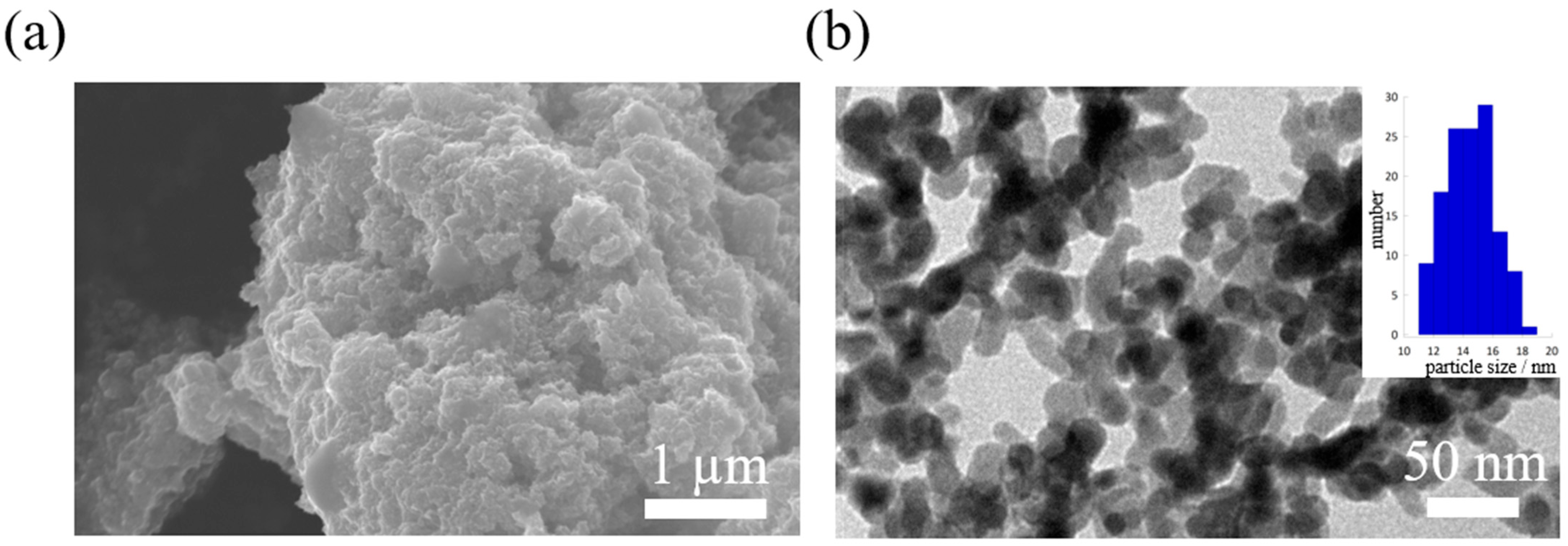
Abstract
:1. Introduction
2. Experimental
2.1. Chemicals
2.2. Synthesis of SnTe Nanocrystal Precursor
2.3. Spark Plasma Sintering
2.4. Characterization
3. Results and Discussion
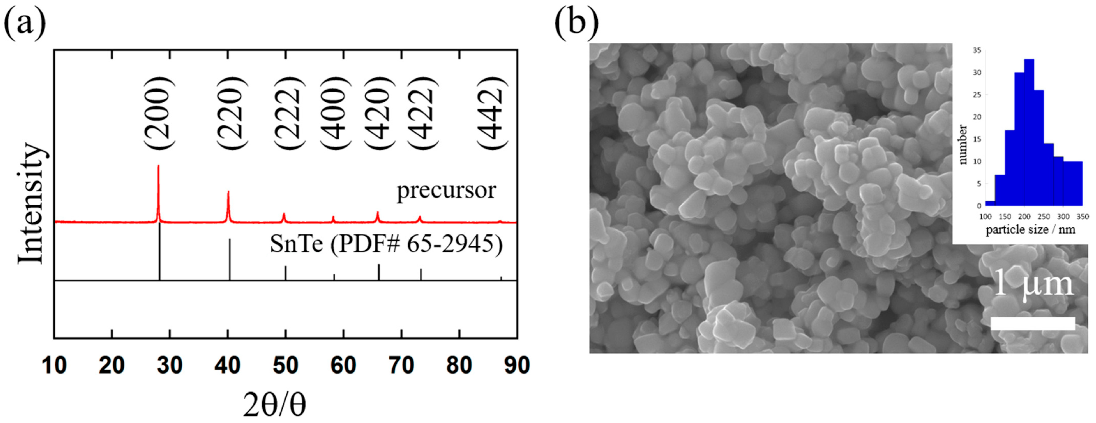
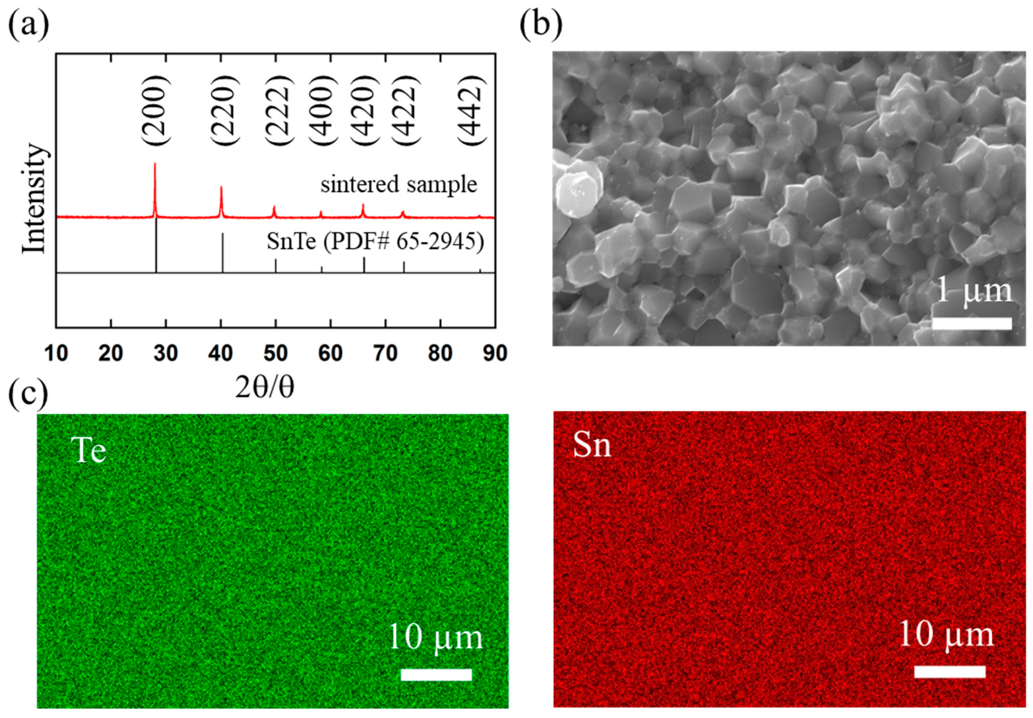
3.1. Characterization of the SnTe Nanocrystal and the Sintered Sample
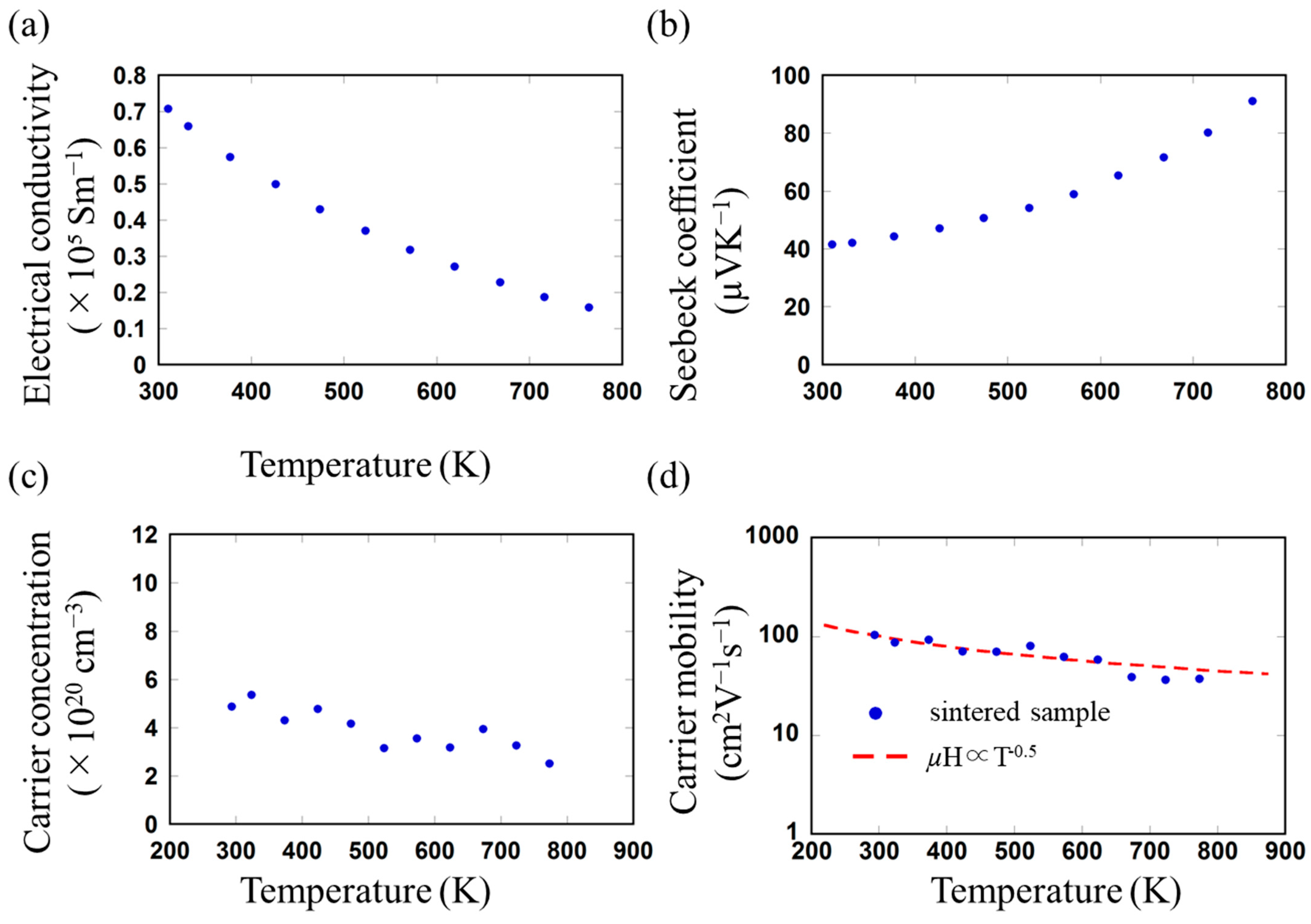
3.2. Electrical Transport Properties
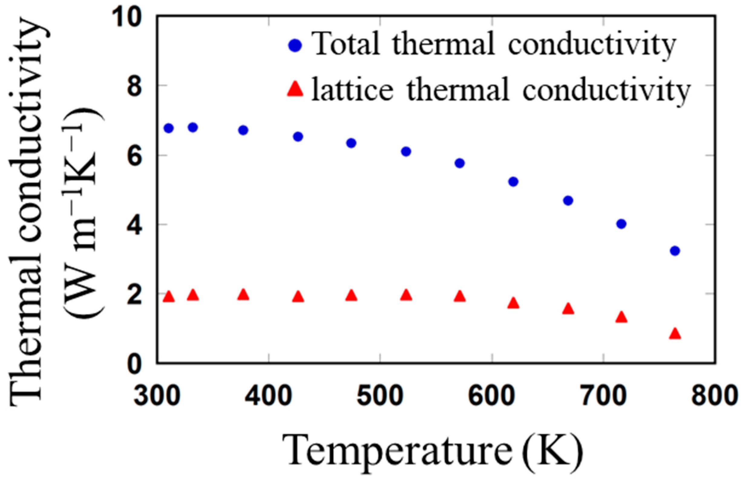
3.3. Thermal Transport Properties
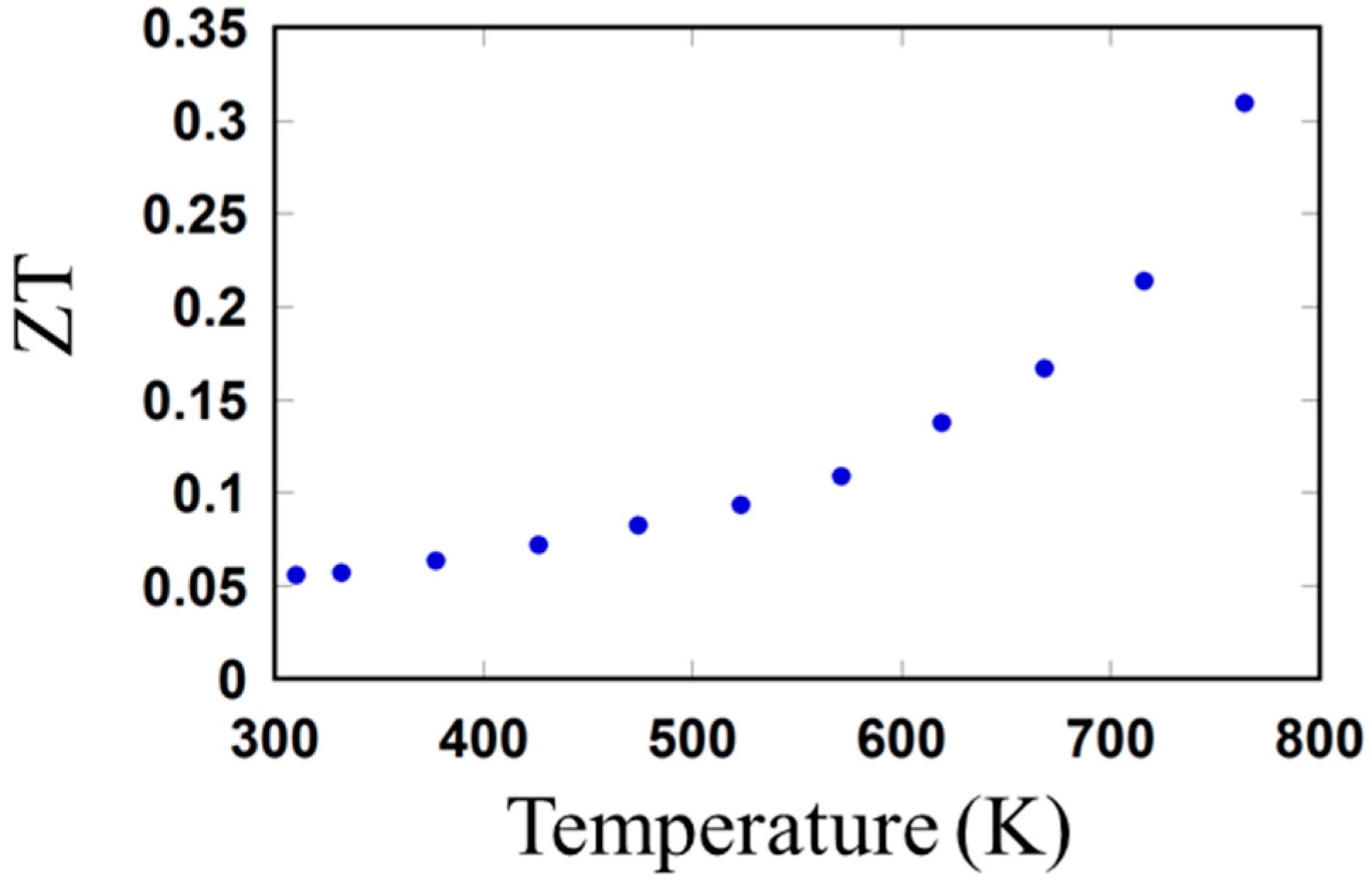
3.4. Figure of Merit
4. Conclusions
Supplementary Materials
Author Contributions
Funding
Data Availability Statement
Conflicts of Interest
References
- Hooshmand Zaferani, S.; Sams, M.W.; Shi, X.-L.; Mehrabian, N.; Ghomashchi, R.; Chen, Z.-G. Applications of Thermoelectric Generators To Improve Catalytic-Assisted Hydrogen Production Efficiency: Future Directions. Energy Fuels 2022, 36, 8096–8106. [Google Scholar] [CrossRef]
- Channegowda, M.; Mulla, R.; Nagaraj, Y.; Lokesh, S.; Nayak, S.; Mudhulu, S.; Rastogi, C.K.; Dunnill, C.W.; Rajan, H.K.; Khosla, A. Comprehensive Insights into Synthesis, Structural Features, and Thermoelectric Properties of High-Performance Inorganic Chalcogenide Nanomaterials for Conversion of Waste Heat to Electricity. ACS Appl. Energy Mater. 2022, 5, 7913–7943. [Google Scholar] [CrossRef]
- Tippireddy, S.; DS, P.K.; Das, S.; Mallik, R.C. Oxychalcogenides as Thermoelectric Materials: An Overview. ACS Appl. Energy Mater. 2021, 4, 2022–2040. [Google Scholar] [CrossRef]
- Abbas, A.; Nisar, M.; Zheng, Z.H.; Li, F.; Jabar, B.; Liang, G.; Fan, P.; Chen, Y.-X. Achieving High Thermoelectric Performance of Eco-Friendly SnTe-Based Materials by Selective Alloying and Defect Modulation. ACS Appl. Mater. Interfaces 2022, 14, 25802–25811. [Google Scholar] [CrossRef] [PubMed]
- Cao, Y.; Bai, H.; Li, Z.; Zhang, Z.; Tang, Y.; Su, X.; Wu, J.; Tang, X. Zn-Induced Defect Complexity for the High Thermoelectric Performance of n-Type PbTe Compounds. ACS Appl. Mater. Interfaces 2021, 13, 43134–43143. [Google Scholar] [CrossRef] [PubMed]
- Tan, G.; Shi, F.; Hao, S.; Zhao, L.-D.; Chi, H.; Zhang, X.; Uher, C.; Wolverton, C.; Dravid, V.P.; Kanatzidis, M.G. Non-Equilibrium Processing Leads to Record High Thermoelectric Figure of Merit in PbTe–SrTe. Nat. Protoc. 2016, 11, 1508–1530. [Google Scholar] [CrossRef]
- Pei, Y.; Tan, G.; Feng, D.; Zheng, L.; Tan, Q.; Xie, X.; Gong, S.; Chen, Y.; Li, J.; He, J.; et al. Integrating Band Structure Engineering with All-Scale Hierarchical Structuring for High Thermoelectric Performance in PbTe System. Adv. Energy Mater. 2017, 7, 1601450. [Google Scholar] [CrossRef]
- Lu, X.; Lu, W.; Gao, J.; Liu, Y.; Huang, J.; Yan, P.; Fan, Y.; Jiang, W. Processing High-Performance Thermoelectric Materials in a Green Way: A Proof of Concept in Cold Sintered PbTe0.94Se0.06. ACS Appl. Mater. Interfaces 2022, 14, 37937–37946. [Google Scholar] [CrossRef]
- Moshwan, R.; Yang, L.; Zou, J.; Chen, Z. Eco-Friendly SnTe Thermoelectric Materials: Progress and Future Challenges. Adv. Funct. Mater. 2017, 27, 1703278. [Google Scholar] [CrossRef]
- Zhang, X.; Wang, Z.; Zou, B.; Brod, M.K.; Zhu, J.; Jia, T.; Tang, G.; Snyder, G.J.; Zhang, Y. Band Engineering SnTe via Trivalent Substitutions for Enhanced Thermoelectric Performance. Chem. Mater. 2021, 33, 9624–9637. [Google Scholar] [CrossRef]
- Ma, Z.; Lei, J.; Zhang, D.; Wang, C.; Wang, J.; Cheng, Z.; Wang, Y. Enhancement of Thermoelectric Properties in Pd–In Co-Doped SnTe and Its Phase Transition Behavior. ACS Appl. Mater. Interfaces 2019, 11, 33792–33802. [Google Scholar] [CrossRef]
- Li, W.; Wu, Y.; Lin, S.; Chen, Z.; Li, J.; Zhang, X.; Zheng, L.; Pei, Y. Advances in Environment-Friendly SnTe Thermoelectrics. ACS Energy Lett. 2017, 2, 2349–2355. [Google Scholar] [CrossRef]
- Wang, L.; Chang, S.; Zheng, S.; Fang, T.; Cui, W.; Bai, P.; Yue, L.; Chen, Z.-G. Thermoelectric Performance of Se/Cd Codoped SnTe via Microwave Solvothermal Method. ACS Appl. Mater. Interfaces 2017, 9, 22612–22619. [Google Scholar] [CrossRef]
- Tian, B.-Z.; Chen, J.; Jiang, X.-P.; Tang, J.; Zhou, D.-L.; Sun, Q.; Yang, L.; Chen, Z.-G. Enhanced Thermoelectric Performance of SnTe-Based Materials via Interface Engineering. ACS Appl. Mater. Interfaces 2021, 13, 50057–50064. [Google Scholar] [CrossRef]
- Moshwan, R.; Shi, X.-L.; Liu, W.-D.; Wang, Y.; Xu, S.; Zou, J.; Chen, Z.-G. Enhancing Thermoelectric Properties of InTe Nanoprecipitate-Embedded Sn1−xInxTe Microcrystals through Anharmonicity and Strain Engineering. ACS Appl. Energy Mater. 2019, 2, 2965–2971. [Google Scholar] [CrossRef]
- Zhou, M.; Gibbs, Z.M.; Wang, H.; Han, Y.; Xin, C.; Li, L.; Snyder, G.J. Optimization of Thermoelectric Efficiency in SnTe: The Case for the Light Band. Phys. Chem. Chem. Phys. 2014, 16, 20741–20748. [Google Scholar] [CrossRef]
- Tan, G.; Shi, F.; Hao, S.; Chi, H.; Bailey, T.P.; Zhao, L.-D.; Uher, C.; Wolverton, C.; Dravid, V.P.; Kanatzidis, M.G. Valence Band Modification and High Thermoelectric Performance in SnTe Heavily Alloyed with MnTe. J. Am. Chem. Soc. 2015, 137, 11507–11516. [Google Scholar] [CrossRef]
- Xu, X.; Cui, J.; Fu, L.; Huang, Y.; Yu, Y.; Zhou, Y.; Wu, D.; He, J. Enhanced Thermoelectric Performance Achieved in SnTe via the Synergy of Valence Band Regulation and Fermi Level Modulation. ACS Appl. Mater. Interfaces 2021, 13, 50037–50045. [Google Scholar] [CrossRef]
- Tan, G.; Zhao, L.-D.; Shi, F.; Doak, J.W.; Lo, S.-H.; Sun, H.; Wolverton, C.; Dravid, V.P.; Uher, C.; Kanatzidis, M.G. High Thermoelectric Performance of P-Type SnTe via a Synergistic Band Engineering and Nanostructuring Approach. J. Am. Chem. Soc. 2014, 136, 7006–7017. [Google Scholar] [CrossRef]
- Zhang, Q.; Liao, B.; Lan, Y.; Lukas, K.; Liu, W.; Esfarjani, K.; Opeil, C.; Broido, D.; Chen, G.; Ren, Z. High Thermoelectric Performance by Resonant Dopant Indium in Nanostructured SnTe. Proc. Natl. Acad. Sci. USA 2013, 110, 13261–13266. [Google Scholar] [CrossRef] [PubMed]
- Banik, A.; Shenoy, U.S.; Anand, S.; Waghmare, U.V.; Biswas, K. Mg Alloying in SnTe Facilitates Valence Band Convergence and Optimizes Thermoelectric Properties. Chem. Mater. 2015, 27, 581–587. [Google Scholar] [CrossRef]
- Banik, A.; Ghosh, T.; Arora, R.; Dutta, M.; Pandey, J.; Acharya, S.; Soni, A.; Waghmare, U.V.; Biswas, K. Engineering Ferroelectric Instability to Achieve Ultralow Thermal Conductivity and High Thermoelectric Performance in Sn1−xGexTe. Energy Environ. Sci. 2019, 12, 589–595. [Google Scholar] [CrossRef]
- Al Rahal Al Orabi, R.; Mecholsky, N.A.; Hwang, J.; Kim, W.; Rhyee, J.-S.; Wee, D.; Fornari, M. Band Degeneracy, Low Thermal Conductivity, and High Thermoelectric Figure of Merit in SnTe–CaTe Alloys. Chem. Mater. 2016, 28, 376–384. [Google Scholar] [CrossRef]
- Pei, Y.; Zheng, L.; Li, W.; Lin, S.; Chen, Z.; Wang, Y.; Xu, X.; Yu, H.; Chen, Y.; Ge, B. Interstitial Point Defect Scattering Contributing to High Thermoelectric Performance in SnTe. Adv. Electron. Mater. 2016, 2, 1600019. [Google Scholar] [CrossRef]
- Wu, H.; Chang, C.; Feng, D.; Xiao, Y.; Zhang, X.; Pei, Y.; Zheng, L.; Wu, D.; Gong, S.; Chen, Y.; et al. Synergistically Optimized Electrical and Thermal Transport Properties of SnTe via Alloying High-Solubility MnTe. Energy Environ. Sci. 2015, 8, 3298–3312. [Google Scholar] [CrossRef]
- Han, G.; Zhang, R.; Popuri, S.; Greer, H.; Reece, M.; Bos, J.-W.; Zhou, W.; Knox, A.; Gregory, D. Large-Scale Surfactant-Free Synthesis of p-Type SnTe Nanoparticles for Thermoelectric Applications. Materials 2017, 10, 233. [Google Scholar] [CrossRef]
- Liu, T.-H.; Zhou, J.; Li, M.; Ding, Z.; Song, Q.; Liao, B.; Fu, L.; Chen, G. Electron Mean-Free-Path Filtering in Dirac Material for Improved Thermoelectric Performance. Proc. Natl. Acad. Sci. USA 2018, 115, 879–884. [Google Scholar] [CrossRef]
- Banik, A.; Vishal, B.; Perumal, S.; Datta, R.; Biswas, K. The Origin of Low Thermal Conductivity in Sn1-xSbxTe: Phonon Scattering via Layered Intergrowth Nanostructures. Energy Environ. Sci. 2016, 9, 2011–2019. [Google Scholar] [CrossRef]
- Zhang, X.; Zhou, Y.; Pei, Y.; Chen, Y.; Yuan, B.; Zhang, S.; Deng, Y.; Gong, S.; He, J.; Zhao, L.-D. Enhancing Thermoelectric Performance of SnTe via Nanostructuring Particle Size. J. Alloys Compd. 2017, 709, 575–580. [Google Scholar] [CrossRef]
- Ma, Z.; Wang, C.; Lei, J.; Zhang, D.; Chen, Y.; Wang, Y.; Wang, J.; Cheng, Z. Core–Shell Nanostructures Introduce Multiple Potential Barriers to Enhance Energy Filtering for the Improvement of the Thermoelectric Properties of SnTe. Nanoscale 2020, 12, 1904–1911. [Google Scholar] [CrossRef]
- Peng, P.; Wang, C.; Li, L.; Li, S.; Chen, J.; Fan, P.; Du, R.; Si, H.; Cheng, Z.; Wang, J. Enhanced Thermoelectric Performance of In-Doped and AgCuTe-Alloyed SnTe through Band Engineering and Endotaxial Nanostructures. Phys. Chem. Chem. Phys. 2022, 24, 27105–27113. [Google Scholar] [CrossRef]
- Wang, L.; Hong, M.; Sun, Q.; Wang, Y.; Yue, L.; Zheng, S.; Zou, J.; Chen, Z.-G. Hierarchical Structuring to Break the Amorphous Limit of Lattice Thermal Conductivity in High-Performance SnTe-Based Thermoelectrics. ACS Appl. Mater. Interfaces 2020, 12, 36370–36379. [Google Scholar] [CrossRef]
- Liu, X.; Zhang, B.; Chen, Y.; Wu, H.; Wang, H.; Yang, M.; Wang, G.; Xu, J.; Zhou, X.; Han, G. Achieving Enhanced Thermoelectric Performance in (SnTe) 1−x(Sb2Te3 )xand(SnTe)1−y(Sb2Se3)y Synthesized via Solvothermal Reaction and Sintering. ACS Appl. Mater. Interfaces 2020, 12, 44805–44814. [Google Scholar] [CrossRef]
- Wang, L.; Zheng, S.; Chen, H. Enhanced Electronic Transport Properties of Se-Doped SnTe1-xSex Nanoparticles by Microwave-Assisted Solvothermal Method. J. Electron. Mater. 2017, 46, 2847–2853. [Google Scholar] [CrossRef]
- Ibáñez, M.; Hasler, R.; Genç, A.; Liu, Y.; Kuster, B.; Schuster, M.; Dobrozhan, O.; Cadavid, D.; Arbiol, J.; Cabot, A.; et al. Ligand-Mediated Band Engineering in Bottom-up Assembled SnTe Nanocomposites for Thermoelectric Energy Conversion. J. Am. Chem. Soc. 2019, 141, 8025–8029. [Google Scholar] [CrossRef]
- Fujiwara, R.; Takashima, Y.; Tsuruoka, T.; Naito, M.; Murai, J.; Akamatsu, K. Chemical Synthesis of Single Nanometer-Sized Bi2−xSbxTe3.0 Nanocrystals via Direct Precipitation Process. Results Chem. 2022, 4, 100485. [Google Scholar] [CrossRef]
- Fujiwara, R.; Takashima, Y.; Tsuruoka, T.; Naito, M.; Murai, J.; Akamatsu, K. High-Performance Bulk Bi0.4Sb1.6Te3.0 Thermoelectrics Prepared from Nanocrystal Precursor Synthesized via Chemical Precipitation. J. Solid State Chem. 2023, 319, 123777. [Google Scholar] [CrossRef]
- Aminzare, M.; Tseng, Y.-C.; Ramakrishnan, A.; Chen, K.-H.; Mozharivskyj, Y. Effect of Single Metal Doping on the Thermoelectric Properties of SnTe. Sustain. Energy Fuels 2019, 3, 251–263. [Google Scholar] [CrossRef]
- Muchtar, A.R.; Srinivasan, B.; Tonquesse, S.L.; Singh, S.; Soelami, N.; Yuliarto, B.; Berthebaud, D.; Mori, T. Physical Insights on the Lattice Softening Driven Mid-Temperature Range Thermoelectrics of Ti/Zr-Inserted SnTe—An Outlook Beyond the Horizons of Conventional Phonon Scattering and Excavation of Heikes’ Equation for Estimating Carrier Properties. Adv. Energy Mater. 2021, 11, 2101122. [Google Scholar] [CrossRef]
- Williamson, G.K.; Hall, W.H. X-ray Line Broadening from Filed Aluminium and Wolfram. Acta Metall. 1953, 1, 22–31. [Google Scholar] [CrossRef]
- Shalvoy, R.B.; Fisher, G.B.; Stiles, P.J. Bond Ionicity and Structural Stability of Some Average-Valence-Five Materials Studied by X-ray Photoemission. Phys. Rev. B 1977, 15, 1680–1697. [Google Scholar] [CrossRef]
- Neudachina, V.S.; Shatalova, T.B.; Shtanov, V.I.; Yashina, L.V.; Zyubina, T.S.; Tamm, M.E.; Kobeleva, S.P. XPS Study of SnTe(100) Oxidation by Molecular Oxygen. Surf. Sci. 2005, 584, 77–82. [Google Scholar] [CrossRef]
- Li, W.; Chen, Z.; Lin, S.; Chang, Y.; Ge, B.; Chen, Y.; Pei, Y. Band and Scattering Tuning for High Performance Thermoelectric Sn1−xMnxTe Alloys. J. Mater. 2015, 1, 307–315. [Google Scholar] [CrossRef]
- Mandava, S.; Basu, R.; Khasimsaheb, B.; Bathula, S.; Muthukumar, V.S.; Singh, A.; Neeleshwar, S. A Synergistic Approach to Achieving the High Thermoelectric Performance of La-Doped SnTe Using Resonance State and Partial Band Convergence. Mater. Adv. 2021, 2, 4352–4361. [Google Scholar] [CrossRef]
- Tan, H.; Guo, L.; Wang, G.; Wu, H.; Shen, X.; Zhang, B.; Lu, X.; Wang, G.; Zhang, X.; Zhou, X. Synergistic Effect of Bismuth and Indium Codoping for High Thermoelectric Performance of Melt Spinning SnTe Alloys. ACS Appl. Mater. Interfaces 2019, 11, 23337–23345. [Google Scholar] [CrossRef]
- Hasezaki, K.; Hamachiyo, T.; Ashida, M.; Ueda, T.; Noda, Y. Thermoelectric Properties and Scattering Factors of Finely Grained Bi2Te3-Related Materials Prepared by Mechanical Alloying. Mater. Trans. 2010, 51, 863–867. [Google Scholar] [CrossRef]
- Gayner, C.; Amouyal, Y. Energy Filtering of Charge Carriers: Current Trends, Challenges, and Prospects for Thermoelectric Materials. Adv. Funct. Mater. 2020, 30, 1901789. [Google Scholar] [CrossRef]
- Heremans, J.P.; Thrush, C.M.; Morelli, D.T. Thermopower Enhancement in PbTe with Pb Precipitates. J. Appl. Phys. 2005, 98, 063703. [Google Scholar] [CrossRef]
- Su, H.; Han, Y.; Xie, L.; Jiang, M.; Wang, Z.; Miao, Z.; Liu, G.; Zhou, M.; Huang, R.; Li, L. Fast Fabrication of SnTe via a Non-Equilibrium Method and Enhanced Thermoelectric Properties by Medium-Entropy Engineering. J. Mater. Chem. C 2023, 11, 5363–5370. [Google Scholar] [CrossRef]
- Li, Z.; Chen, Y.; Li, J.-F.; Chen, H.; Wang, L.; Zheng, S.; Lu, G. Systhesizing SnTe Nanocrystals Leading to Thermoelectric Performance Enhancement via an Ultra-Fast Microwave Hydrothermal Method. Nano Energy 2016, 28, 78–86. [Google Scholar] [CrossRef]
- Kim, H.-S.; Gibbs, Z.M.; Tang, Y.; Wang, H.; Snyder, G.J. Characterization of Lorenz Number with Seebeck Coefficient Measurement. APL Mater. 2015, 3, 041506. [Google Scholar] [CrossRef]
- Mehta, R.J.; Zhang, Y.; Karthik, C.; Singh, B.; Siegel, R.W.; Borca-Tasciuc, T.; Ramanath, G. A New Class of Doped Nanobulk High-Figure-of-Merit Thermoelectrics by Scalable Bottom-up Assembly. Nat. Mater. 2012, 11, 233–240. [Google Scholar] [CrossRef] [PubMed]
- Vineis, C.J.; Shakouri, A.; Majumdar, A.; Kanatzidis, M.G. Nanostructured Thermoelectrics: Big Efficiency Gains from Small Features. Adv. Mater. 2010, 22, 3970–3980. [Google Scholar] [CrossRef] [PubMed]


Disclaimer/Publisher’s Note: The statements, opinions and data contained in all publications are solely those of the individual author(s) and contributor(s) and not of MDPI and/or the editor(s). MDPI and/or the editor(s) disclaim responsibility for any injury to people or property resulting from any ideas, methods, instructions or products referred to in the content. |
© 2023 by the authors. Licensee MDPI, Basel, Switzerland. This article is an open access article distributed under the terms and conditions of the Creative Commons Attribution (CC BY) license (https://creativecommons.org/licenses/by/4.0/).
Share and Cite
Fujiwara, R.; Ikeda, Y.; Kawaguchi, T.; Takashima, Y.; Tsuruoka, T.; Akamatsu, K. Structure and Thermoelectric Characterization of p-Type SnTe Nanobulk Material Synthesized by Charge Compensation Chemical Reaction. Energies 2024, 17, 190. https://doi.org/10.3390/en17010190
Fujiwara R, Ikeda Y, Kawaguchi T, Takashima Y, Tsuruoka T, Akamatsu K. Structure and Thermoelectric Characterization of p-Type SnTe Nanobulk Material Synthesized by Charge Compensation Chemical Reaction. Energies. 2024; 17(1):190. https://doi.org/10.3390/en17010190
Chicago/Turabian StyleFujiwara, Ryosuke, Yuta Ikeda, Takuto Kawaguchi, Yohei Takashima, Takaaki Tsuruoka, and Kensuke Akamatsu. 2024. "Structure and Thermoelectric Characterization of p-Type SnTe Nanobulk Material Synthesized by Charge Compensation Chemical Reaction" Energies 17, no. 1: 190. https://doi.org/10.3390/en17010190