Article

Analysis of Space Charge Signal Spatial Resolution Determined with PEA Method in Flat Samples including Attenuation Effects

Department of Electrical and Power Engineering, Faculty of Electrical Engineering, Automatics, Computer Science, and Biomedical Engineering, AGH University of Science and Technology, al. Mickiewicza 30, 30-059 Kraków, Poland
*
Author to whom correspondence should be addressed.
Energies 2023, 16(8), 3592; https://doi.org/10.3390/en16083592
Submission received: 21 February 2023 / Revised: 24 March 2023 / Accepted: 19 April 2023 / Published: 21 April 2023

Abstract

:
The constant development of the electrical engineering sector, especially in the transmission of electrical energy under high-voltage direct current (HVDC), requires research on new insulation materials and investigations of physical phenomena under ultrahigh electrical fields in solid dielectrics. One of the current problematic issues is the formation of space charge in HV insulation systems, which affects the operational electrical field distribution and can lead to faster insulation degradation. There are several problems that have to be considered before every space charge measurement, such as the attenuation and dispersion of sound waves in tested dielectric materials, reflections at the interfaces, and the spatial resolution of the measured charge profile. The spatial resolution is one of the most important technical factors of the PEA measurement stand. The spatial resolution, as it is assumed, depends on several factors, such as the width of the pulser and the pulse rise time, the thickness of the piezoelectric sensor, and the dispersion of the tested material. The article presents the laboratory measurement results of the impact of pulser parameters, such as pulse width and rise time, and sensor thickness on the equivalent thickness of the measured net charge layer corresponding to the resolution of the method. The dispersion in the tested LDPE material is also presented and analysed. The results show that with an increase in the pulser rise time, a higher resolution of the pea method can be achieved.

1. Introduction

The constant development of the electrical engineering sector, especially in the transmission of electrical energy under high voltage direct current (HVDC), requires research on new insulation materials and investigations of physical phenomena under ultrahigh electrical fields in solid dielectrics. The application of smart materials, such as field-grading materials [1] or self-healing materials [2] in HVDC systems can elevate their reliability. HVDC systems are a common research area with AC solid insulation systems such as partial discharges [3,4] and lightning protection [5], which are well-studied in many research centres. Partial discharges constantly deteriorate the insulation systems [3,5,6,7] and can be a source of space or surface charge [8]. There are several factors affecting the generation of discharges, such as pressure, temperature, harmonic content [3,4,6], and even the presence of a magnetic field [9]. One of the possibilities for the determination of surface charge generated by the partial discharges or corona is a scan of the dielectric sample surface with the electrostatic voltmeter [8,10].
One of the current problematic issues is the formation of space charge in insulation systems, which affects the operational electrical field distribution and can lead to faster insulation degradation and, in the worst case, insulation damage. This topic is very common in the research fields of HVDC cables and cable accessories [11], DC gas insulated systems (GIS) spacers [12], and other subjects not related to high voltage transmission such as charging of spaceships in isolation [13], e-mobility [14], and electric aircraft [14]. The investigation of space charge distribution can be performed with the use of several non-invasive methods, which are mainly based on the generation of a pressure wave in the test material. The origin of the force that acts on the charge can be different [15,16,17]. In the piezoelectric induced pressure wave propagation (PIPWP) method, the piezoelectric source acts as a stimulus; in the laser-induced pressure wave propagation (LIPP) method, the laser rays provide the travelling pressure wave in the material; in the thermal step method (TSM), a heat wave is a stimulus that allows the measurement of the electric charge. The most commonly used method is the pulsed electro acoustics (PEA) method, in which the stimulation force is generated by the transition of the electrical field provided by the pulser. The PEA method is most promising in the cases of sensitivity and resolution and has applicability not only in laboratory conditions but in future works on field measurement [18]. The research in the field of space charge measurement in dielectric materials with the PEA method was developed in the 1980s, when Takada et al. [19] proposed this method. In subsequent years, the method was constantly developed and improved with the application of the deconvolution technique [20,21], the replacement of LiNbO3 sensors with polarised polyvinylidene fluoride PVDF [22], or the modification of the measurement stand for better coupling of the acoustic wave (i.e., the usage of a semicon at the HV electrode, the application of a polymer coupling element between the ground electrode and sensor [23]), usage of the sample as coupling capacitance for pulser application [24], especially during testing cables at nominal voltage [25]. Most research interests cover the fundamental science of analysis of the formation mechanism of space charge in solid dielectrics used in the cable industry, such as polyethylene, silicon rubber, and PCV. The samples under test might be single-layer flat samples, multilayer homogenous samples, or multilayer samples with different materials. The formation of space charge in a dielectric sample depends on the charge transport process, which is affected by the value of the electrical field and ambient conditions, especially temperature [26,27,28,29,30,31]. The application area of research focuses on the formation and analysis of space charge in mini cables [11], full-scale cables [11,23,25,32], and accessories [33], the impact on polarity reversal [34], which might happen during HVDC station operation, and the impact of a temperature gradient, which appears naturally during cable operation [35]. The methodology of space charge investigations in cables below 500 kV is standardised by IEEE [36]. The research is conducted both in laboratory research and by analytic or numerical approaches [11,37,38]. The divagations in the field of studies are also conducted for the improvement of the calibration process [38,39,40] and deconvolution methodology [21,41], especially in thick and very attenuated samples [42]. Several problems have to be considered before every measurement, such as attenuation and dispersion of sound waves in tested dielectric materials, reflections at the interfaces [37], and the spatial resolution of the charge determination along the sample. The spatial resolution is one of the most important technical factors of the PEA measurement stand. The CIGRE TB 288 [16] proposes the relation for the spatial resolution determination, but it is very simplified and takes into consideration only the pulser width and the sample thickness. The spatial resolution, as it is assumed, depends on several factors, such as the width of the pulser and the pulser rise time, the thickness of the piezoelectric sensor, and the dispersion of the tested material. The CIGRE assumption is to operate with a resolution of 2–5% of sample thickness, which can be insufficient in the case of thick samples and multilayer samples. The better the resolution, the more sharply the hetero- or homo-charges can be detected; for poor resolution, the charges placed in the vicinity can be the origin of the wide wavelets that reduce the resolution of the equivalent thickness of the charge layer. There is much research on the resolution of the PEA method; in [20], authors achieved spatial resolution in the range of 3 µm for 100 µm thick samples and a 4 µm sensor; the best resolution was achieved in [43] and was equal to 1.7 µm authors used the 1 µm PVDF sensor for a 25 µm sample; authors in [44] presented results with 7 µm resolution for a 125 µm sample and a 1 µm sensor with a 5 ns wide pulse. The research conducted in [45] covers the analysis of spatial resolution for a PMMA sample with 1 µm thickness; the application of deconvolution sharpens the resolution by a factor of 6 to 10 ns. For the thick samples, especially for mini cables or full-scale cables, the thick PVDF sensors (100 µm, 125 µm) and the wider pulses (tw = 400 ns) are applied in measurements [33]. The thicker sensor gives a higher signal at the conversion of the mechanical wave to a measurable electrical signal. Most research information on the PEA spatial resolution is based on experimental results and does not provide a comprehensive guideline for the achievement of the golden ratio between the best resolution and the highest measured PEA signal.
The article is organised as follows: First, the most important and current achievements in the pulsed electroacoustic area are presented. The second chapter presents the PEA measurement stand for the determination of charge profiles of flat dielectrics. The third paragraph presents the investigation results for the impact of the measurement stand parameters on the spatial resolution and attenuation phenomena. The final sections are a discussion and conclusion about the presented results. The earlier investigations [46] showed a positive correlation between pulser rise time and its gradient on the shape of the charge signal wavelet generated in the sample; most of the articles correlate the resolution with the pulser duration, not the rise/fall times. This article focuses in a compendious way on the analysis of pulser parameters, sensor thickness, and semi-conductive layer electrical properties and their influence on spatial resolution. The conclusions are based on the laboratory measurement results of the space charge profile determined for different pulser parameters, such as pulse width and rise time, sensor thickness, and semiconductive layer parameters. The analysis was focused on the change in equivalent thickness of the measured net charge corresponding to the resolution of the method and dispersion in the dielectric material. The test object was flat samples made from Kapton HN® and LDPE (low-density polyethylene) with variable thickness.

2. Pulse Electro Acoustic Method

2.1. Method Overview

The pulsed electro acoustics method is based on the measurement of pressure waveforms generated by the electrical charges inducted in the dielectric sample by the HV applied to the test sample. The short-duration pulser stimulates the movement of the charges, which implies travelling pressure waves. The waves are forming in both directions of charge movement, reflecting from the surfaces with different acoustic impedances. The waves propagate at a speed specific to the particular material. Different materials provide different attenuation and dispersion of waves (different frequencies travel at different speeds), and this is especially visible for thick samples >1 mm. The wave is transformed into an electrical signal by the piezoelectric sensor, which is mostly PVDF. The nanosecond wavelets of the pressure wave are transformed almost without a change in shape due to the ultra-wideband response of PVDF. The acquisition of this electrical signal as a time series signal allows one to determine the space charge profile in the sample. To avoid the impact of the measurement setup, the deconvolution technique is necessary.
The investigations of the formation of space charge in samples are divided into two main subjects: basic studies that identify the process of charge transport in analysed materials, the impact of the instrumentation on the quality of the results, and investigations of other factors (i.e., temperature, material modification) that can change the space formation process. For this investigation, the setup for measurement in flat samples should be employed. In this case, the theoretical analysis is more efficient. The second subject of pea measurement is a measurement on real geometry test objects; this is performed on cylindrical geometry objects, which are cable systems. In this case, the material and the manufacturing process that impact the space charge formation are analysed.
The algorithm for the determination of space charge in flat samples is presented in Figure 1. The steps for determining the space charge profile are as follows: The sample preparation and conditioning for the disposal of the residual charges can be achieved by the sample discharging between metal electrodes, cleaning the sample with isopropanol alcohol, and heating the sample to a temperature below operating conditions at which it will discharge naturally [47]. The determination of the charge profile is made by the application of pulser voltage and HVDC. Due to the polarisation process, an electrical charge accumulates at the HV and GND electrodes, which is easily detectable by the measurement stand. At high electrical fields (more than several dozen kV/mm), which are generated in the sample by the HVDC source, charge migration to the sample interior appears. This charge can be detected by the change in the measured pea profile. For the results to be sharpened, the deconvolution process is necessary. Some aspects of the deconvolution procedure for homogeneous flat samples and nonhomogeneous samples are discussed in [21]. The calibration process allows for a deconvoluted result in the C/m3 unit. Calibration is based on the integration of charge accumulated at the ground electrode when there is no space charge in the sample and with known HVDC voltage, the scaling factor is calculated with (1). The integration of the pea profile is made on the charge wavelet from the GND electrode in the range of x0 (assumed as the point where the wavelet begins) to xGND (assumed as the point where the wavelet ends). The charge signal from the GND electrode has the smallest attenuation and dispersion because it travels only through the metal electrode. In the literature, consideration of the pulser in the calibration process is reported [39]. The surface charge density along the sample thickness is achieved by the integration of the space charge profile. The analysis of electrical field distribution is made on the basis of the surface charge density profile and its deformation over time as a high electrical field acts on the sample.
c = ε 0 ε r U D C d 1 x 0 x G N D p e a ( x , 0 ) d x
σ ( x , t ) = c p e a ( x , t ) d x
E x , t = σ x , t ε 0 ε r
The spatial resolution is one of the most important parameters of the measurement setup, according to [16], the spatial resolution expressed as a % of sample thickness can be determined by Equation (4).
η = t w d v 100 %
where:
η —relative resolution depending on the sample thickness, %,
t w —pulse voltage time width [s],
d —sample thickness [m],
v —speed of sound waves in tested material [m/s]

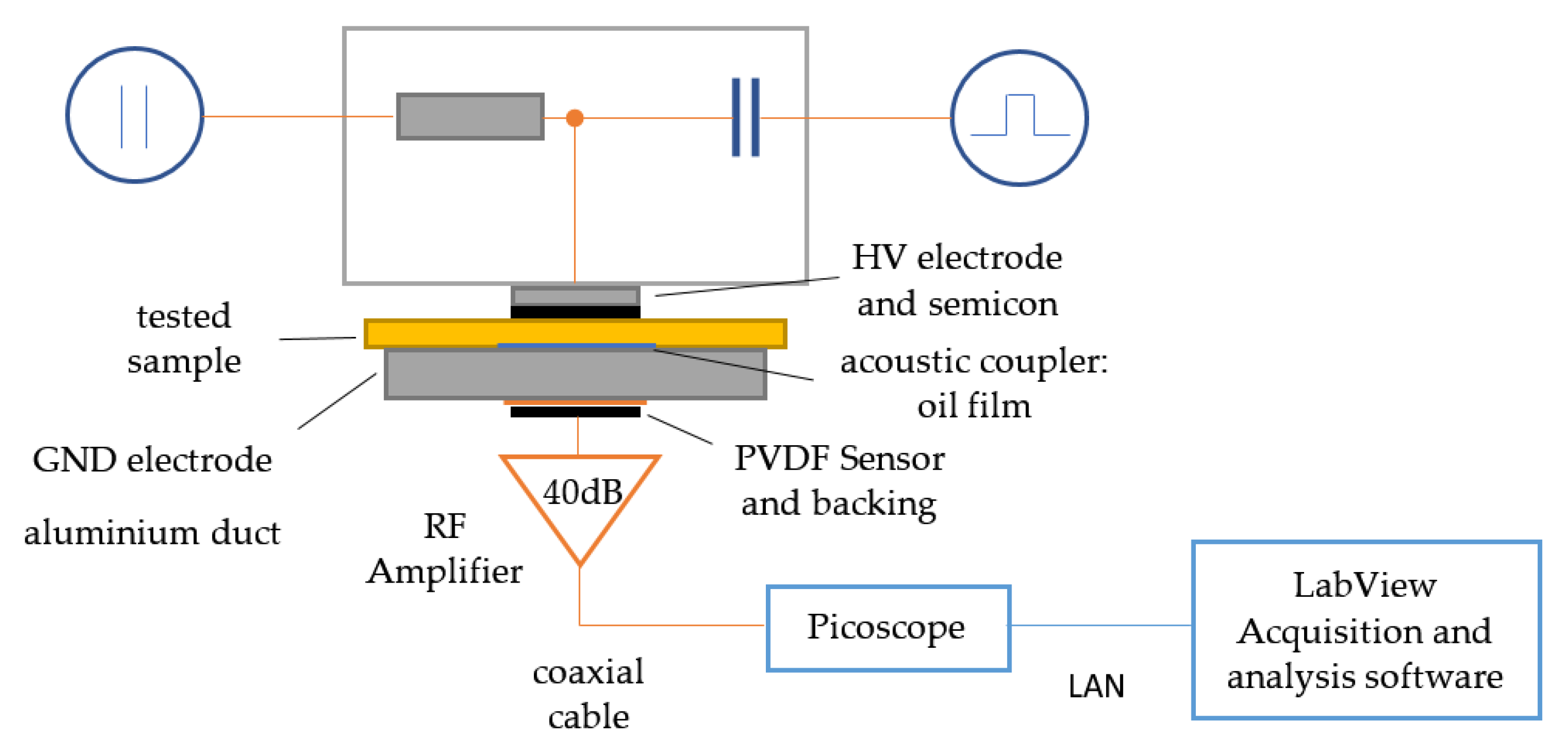
2.2. Measurement Stand for PEA Method

In the PEA (pulsed electro acoustics) method, the conversion between the acoustic waves travelling in the material and the detectable electrical signal is made by the piezoelectric converter; in most cases, a PVDF sensor is used. The PEA stand for measurement of charge profile was equipped with several sets of PVDF sensors with different thicknesses ds 3 µm, 9 µm, 28 µm, 52 µm, and 100 µm. The sensors have an impact on the signal strength and the shape of the response. PVDF has a wide band response and is thus suitable for the detection of nanosecond mechanical wavelets. The amplification of the signal is necessary, so a 9 kHz–3 GHz, 40 dB amplifier was used. The stand was equipped with a HV DC voltage source, the Glassmann model FJ10R12. The two sets of pulsers were: a fast-rise time pulser (rise time tr = 1 ns) with variable time width tw = 1 ns to 5 ns and voltage up to 2 kV, and a variable-rise time pulser (tr = 8–20 ns) with variable pulser width tw = 20–100 ns and voltage up to 1.7 kV. The signal acquisition was made by PicoScope with a sampling rate of 5 GS/s and a bandwidth of 1 GHz. To match the acoustic impedance and improve the visibility of charge at the HV electrode, a semiconductive layer with a resistance of 400 Ω was used. The improvement of the acoustic coupling between the GND electrode and the sample was made by the thin silicon oil film [47]. The schematic of the used measurement stand is shown in Figure 2. The acquisition of pea waveforms was made with 200 averaged waves.

3. Experiment Description

The aim of the experiment was to show the impact of pulser parameters and sensor thickness on measurement sensitivity and resolution of charge distribution in flat dielectric samples. The dispersion and attenuation of the measured wave in relation to sample thickness were also presented. The methodology was to measure the pea waveforms in the test samples with different pulse widths under the same voltage conditions. The pulser voltage was set to 1.3 kV. The different sensor thicknesses were used for the conversion of an acoustic wave to an electrical signal.

Materials Used in Investigations

The samples had form of the flat single layer or double layer samples consisted of LDPE or Kapton HN® [48]. The thickness of the samples varied from 0.1 mm up to 2 mm. The basic mechanical and electrical properties of used materials are listed in Table 1.

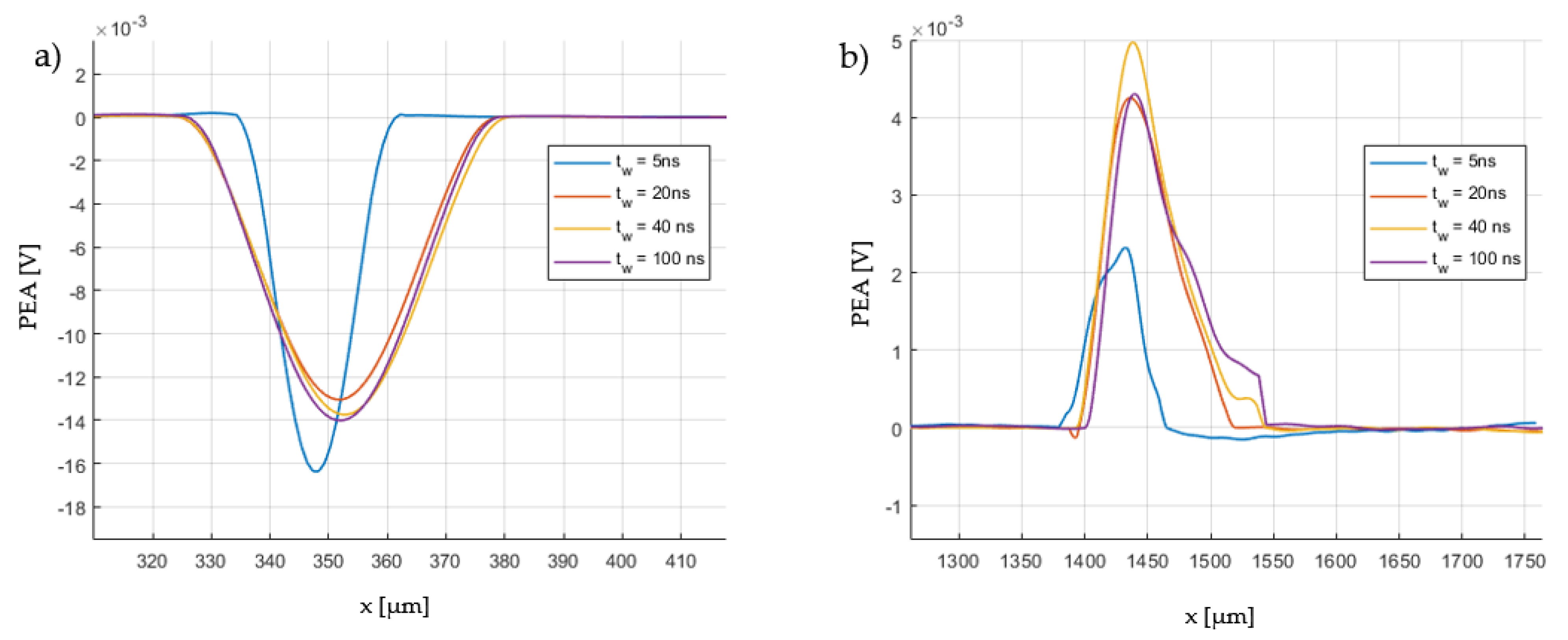
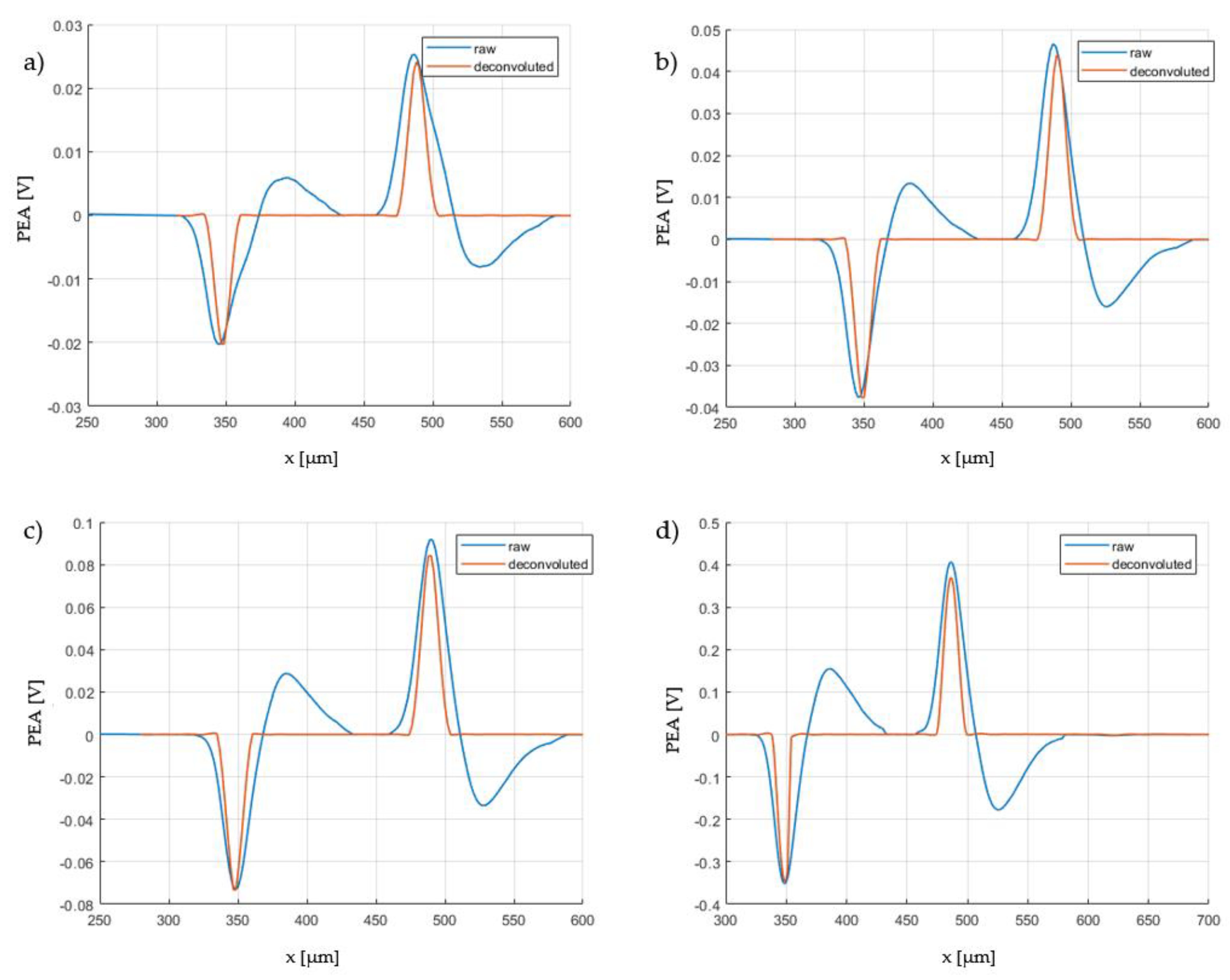
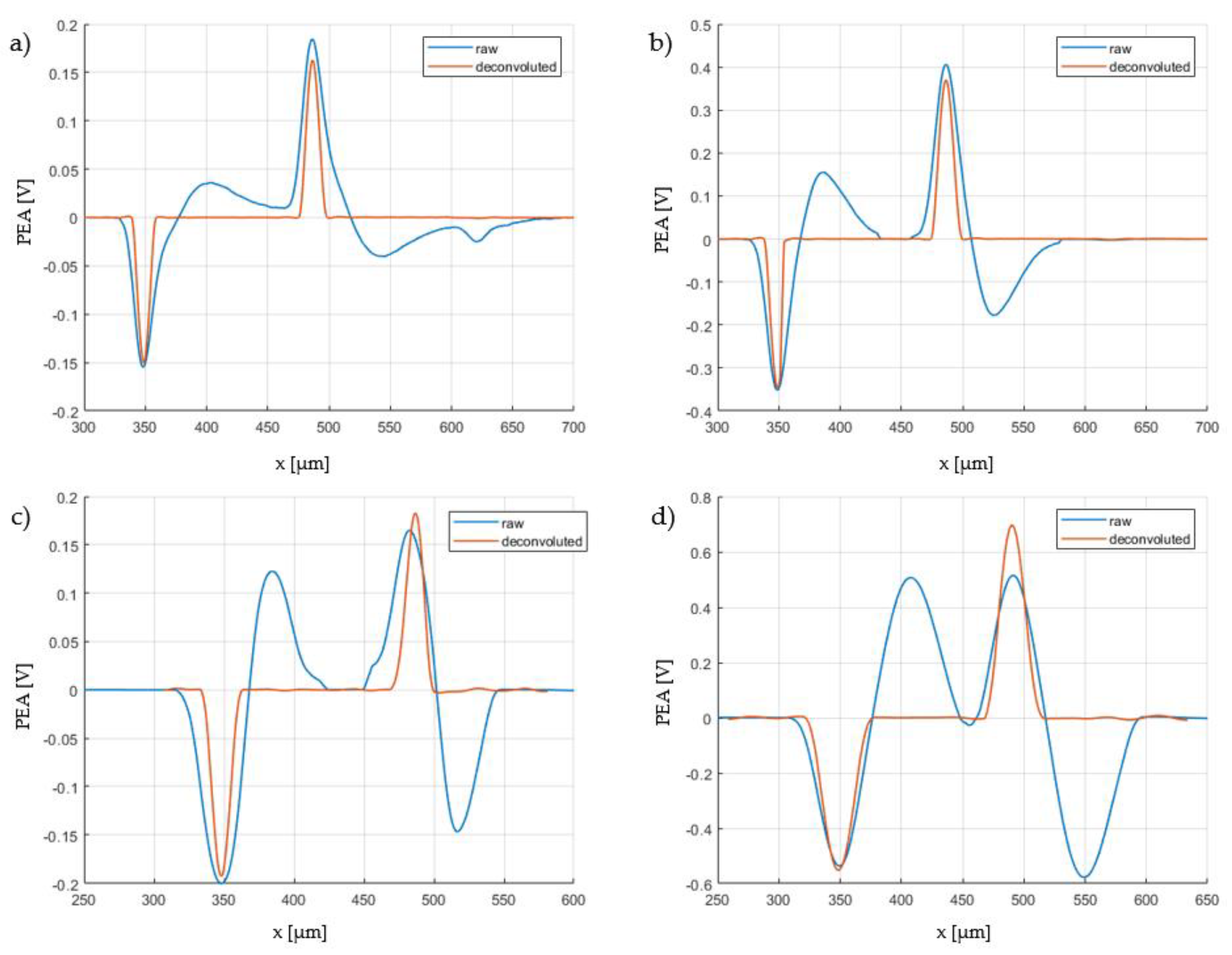
4. PEA Waveforms Measurement Results
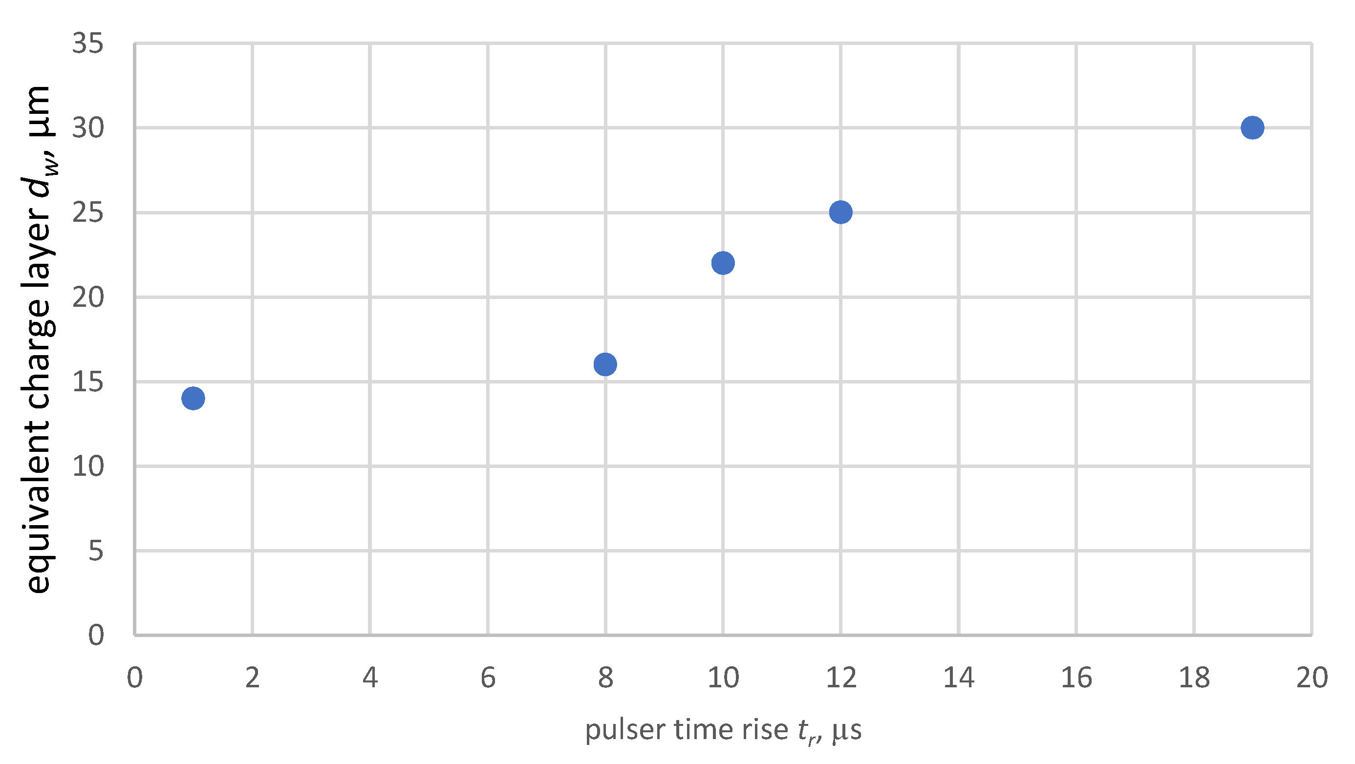
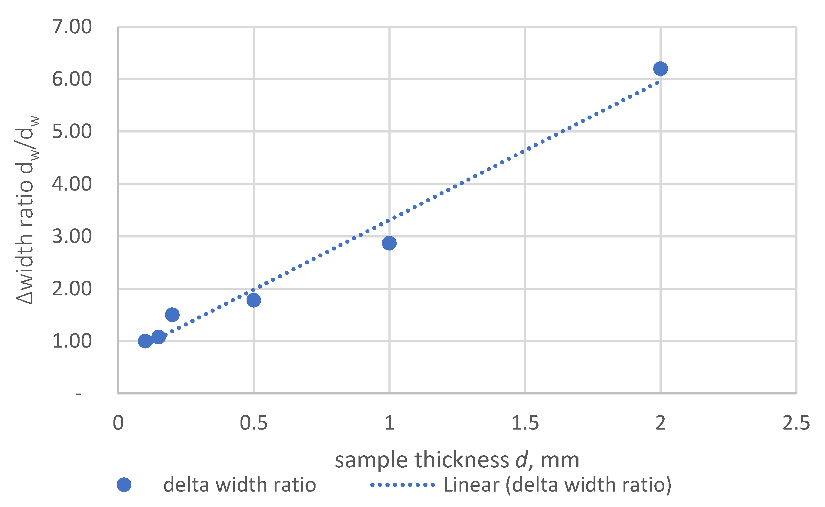
The results of raw pea waveforms and after deconvolution are presented in figures in this section. The deconvolution sharpens the charge profile. The results present the pea profile waveforms in V units before calibration. The resolution of the method impacts the calibration process because of the use of a wider or thinner wavelet in calculations.
Figure 3 presents the pea waveforms measured for a 1 mm thick LDPE sample. The measurements were for pulser width with tw = 5 ns and rise time tr = 1 ns, and with a second pulser with variable width tw = 20, 40, and 100 ns and constant rise time tr = 18 ns. The results were obtained for a PVDF sensor with a thickness of 9 μm.
The summary of the deconvoluted results for different pulser widths is presented in Figure 4. It can be seen that different pulser widths for the sensor (9 μm) provide the same profile of the charge at the ground and high voltage electrodes. There is a difference with the 5 ns pulser because it has a faster rise time. Similar investigation results are presented in Figure 5. In this case, the pulser with tr = 1 ns was used with smaller pulse widths equal to 1, 2, 4, and 5 ns. The test sample was single-layer kapton with a thickness of d = 0.15 mm. The analysis of the result shows no impact of pulser width on the charge profile at the GND and HV electrodes for the 9 μm sensor. Only the measured signal amplitude, especially for the HV electrode, is varying.
Due to the fact that the sensor parameters determine the measured voltage response, the impact of the sensor thickness ds was also analysed. The results of the pea waveforms determined for different sensor thicknesses (ds 3 μm, 9 μm, 28 μm, and 52 μm for 0.15 mm Kapton) are presented in Figure 6. The pulser used for this measurement was tw = 5 ns and tr = 1 ns. The sensor thickness has an influence on the measured electrical response to the mechanical wave generated by the charge movement. The maximal values are lower for the thinner sensors, and the response is wider for the thinner sensors. The obtained equivalent thickness of the charge layer dw varies from 14 μm up to 30 μm.
The last set of measurements was based on the pea waveforms for different thickness samples; in this case, LDPE of different thickness was used. The results are presented in Figure 7. The 9 μm sensor and the pulser with tr = 18 ns and tw = 40 ns were used. The obtained results show the dispersion and attenuation of the pea signal generated by the charge at the HV electrode. It can be noticed that the ratio of the HV charge amplitude to the GND charge amplitude falls with the increase in sample thickness, as does the ratio of charge width. It was noted that sample thickness does not impact the resolution of the equivalent charge layer thickness at the GND electrode.

5. Discussion

One of the most important aspects of the determination of the space charge profile in the dielectric sample is the resolution of the method used. The resolution depends on the parameters of the devices. The CIGRE 288 TB [11] proposes the relation for determination of the measurement resolution (4). Based on the pulser width and sample thickness, this theory is too weak because it does not consider the pulser rise time, sensor width, and broadband simplifier parameters. One of the indicators of the resolution is the width of the wavelet signal related to the charge in the sample, in this article called equivalent charge layer dw. The equivalent charge layer dw was measured for the GND signal due to the lack of dispersion and attenuation issues for this wavelet. The summary of the impact of pulser width on the resolution of equivalent charge layer dw thickness is presented in Figure 8. In the investigations, the charge wavelet width dw was measured at 50% of the amplitude at rising and falling slopes. The resolution determines the minimal width at which a space charge can be detected. It can be seen that for the pulser with the constant rise time tr and variable width tw, the value of the measured equivalent charge layer is constant for the analysed 9 μm thick sensor. The time of flight of a sound wave through a 9 μm PVDF sensor is approximately 4 ns. For pulser widths shorter than the mechanical wave time flight through the sensor, the pulser width might also impact the equivalent charge layer. For pulsers with a rise time tr longer than the time flight through the sensor, the pulser width tw does not influence the resolution. For the pulsers with a shorter rise time/time width than the time flight through the sensor, the reflection phenomena in the sensor impact the obtained results, lowering the measurement resolution. The reason for which this is not visible for the 9 μm sensor and the pulse widths below 4 ns is the fact that the measurement head (Figure 2) consists of a coupling capacitor and a semicon, and the capacitance of the sample acts as a low-pass filter, slowing the pulser rise time as it appears directly at the sample. The calculations of the pulser shape directly on the sample are presented in Figure 9. It can be seen that for the fast rise time pulser (1 ns), the signal at the sample appears with the slower slope for high ohmic semicons, and for the 1000 ohm semicon, the rise time is 6 ns. Thus, for a 400 ohm semicon, 9 μm sensor, and pulser with tw = 1–5 ns, the results were not affected by the pulser width. The authors of article [49] propose to bypass the semicon with thin aluminium foil, which lowers the impedance between the HV electrode and the sample.
Figure 10 presents the comparison of the measured 40 ns width pulser signal, its gradient, and the resultant PEA signal from the charge at the GND electrode. As can be seen, the PEA wavelet shape corresponds to the gradient of the pulser. The pulser gradient reflects the electrostatic force that acts on the charges. The time width tw of the pulser does not have an impact on the change in the force that acts on the charges in dielectrics.
In the second pulser used, the rise time of the square wave output was tunable, and the results of the resolution of equivalent charge layer thickness dw in relation to pulser rise time tr are shown in Figure 11. The results consist of the results for the first pulser and the tunable second pulser. The results clearly present the relation between the impact of the rise time of the pulser and the equivalent charge layer thickness. The test object was 1 mm of LDPE and a 9 µm sensor. The pulsed electrical field stimulates the charge to cause movement, which provides the elastic waves in the material sample. The acoustic wave is proportional to the rate of change of pressure, which relates to the rate of change of force over time. The faster the time increases, the better the resolution of the measured equivalent charge layer. For a 9 μm PVDF, the thinnest charge layer for the pulser with tr 1 ns was measured at 14 μμm.
The piezoelectric sensor is a key element in the conversion of the elastic waves into a measurable electrical signal; its properties, such as wideband response, are important for the resolution and sensitivity of the measurements. The analysis presented in Figure 12 shows the influence of the senor thickness on the equivalent charge layer dw. It can be seen relation between the spatial resolution and sensor thickness. The response of the sensor is much broader for thicker sensors due to its dimensions and mechanical inertia.
The dispersion problems are important due to the sensitivity of the measurement, especially for the thick samples, and the charge transportation process at the region of HV electrodes. The attenuation in the sample impacts the amplitude of the measured signal. The attenuation is related to the sample structure; metals such as aluminium electrodes have the smallest attenuation of the mechanical waves. In dielectrics, due to their atomic structure, the dispersion is more visible. Figure 13 shows the ratio of the amplitude of the HV electrode to the GND electrode in the absence of any space charge formation in the sample; this figure shows only the attenuation effect in the LDPE material. This result was obtained for a ds = 9 μm sensor and a tw = 5 ns pulser with a tr = 1 ns. It can be noticed, that the charge signal at the HV electrode is more damped for the thicker samples. This relation is not linear. The ratio of the charge wavelet width of the HV side to the GND side is shown in Figure 14. This result was obtained for a tw = 5 ns pulser with a rise time of tr = 1 ns and ds = 9 μm PVDF sensor. The wider the signal at the HV electrode, the smaller the spatial resolution. It can be noted that dispersion lowers the spatial resolution depending on the sample thickness, even up to six times for a 2 mm thick sample; thus, the resolution is not constant over sample thickness. The thicker samples provide a more dispersed signal travelling through the sample.
Figure 15 shows the ratio of the amplitude of the HV electrode to the GND electrode with relation to the pulser width for a ds = 9 μm sensor. It can be seen that for wider pulsers, the amplitude of the HV electrode gains value in relation to the GND charge signal. In the absence of damping and dispersion, these two amplitudes should be equal.
The elastic waves are generated in the samples in time instances equal to the transition times of the pulser at the positive and negative slopes. The positive force is generated by the rising voltage from 0 to Upulser, and the negative force is generated when the pulser voltage drops to zero. In this case, two elastic waves are generated and travel across the sample with a distance equal to the relation between pulse width and speed of sound in material tw·v. The dispersion in dielectric material causes a reduction in the steepness of travelling sound waves. Thus, two elastic wavelets might interfere depending on the tw and the pulse rise time tr. For longer pulse widths and thicker samples, the interference of the elastic waves is much smaller, causing a higher measured signal at the piezoelectric transducer.

6. Conclusions

The measurement of the space charge profile in dielectric samples is an important procedure in the development of reliable HVDC cables and accessories. Several research groups are still improving this method to achieve the best resolution and sensitivity. This article presents key issues with the measurement of the space charge profile in flat sample dielectrics. The sensor thickness should be selected in an optimal way to achieve the preferred spatial resolution and the highest measurement signal; the thinner the sensor, the better the spatial resolution, regarding the sample thickness. Additionally, the results prove that pulser rise time has an important impact on the resolution; a shorter pulser rise time provides a better resolution and a higher measured signal. This also has to be matched with the coupling capacitor in the measurement head of the PEA system and semicon parameters due to the low-pass filtering nature of RC circuits. In cases where the sensor thickness has a longer time of flight than the pulser width, the pulser width and rise time might have an impact on the spatial resolution. For sensors with a shorter time flight than the pulser width, the pulser width has no impact on the spatial resolution. For thick samples, the pulser width should be tuned to achieve the highest signal generated by the charge that occurred in the region of the HV electrode. Due to the dispersion effect in a dielectric material, the resolution of the measured signal induced by the charge at a further distance from the sensor falls. This means that the resolution of the determination of charge inside the sample is smaller than that calculated at the GND electrode.

Author Contributions

Conceptualization and methodology, M.F. and M.K.; formal analysis, M.F. and M.K.; investigation and resources, M.F. and M.K.; data curation, M.F. and M.K.; writing—original draft preparation, M.F. and M.K.; visualisation, M.F. and M.K.; supervision and project administration, M.F. and M.K. All authors have read and agreed to the published version of the manuscript.

Funding

This research received no external funding.

Data Availability Statement

Not applicable.

Conflicts of Interest

The authors declare no conflict of interest.

References

  1. Rachmawati; Kojima, H.; Kato, K.; Zebouchi, N.; Hayakawa, N. Electric Field Grading and Discharge Inception Voltage Improvement on HVDC GIS/GIL Spacer with Permittivity and Conductivity Graded Materials (ε/σ-FGM). IEEE Trans. Dielectr. Electr. Insul. 2022, 29, 1811–1817. [Google Scholar] [CrossRef]
  2. Li, Y.; Wang, Y.; Li, Y.; Zhang, Y.; Yaseen, A. Research on Space Charge Characteristics of LDPE/Microcapsule Self-healing Insulation Material. In Proceedings of the 2021 International Conference on Electrical Materials and Power Equipment (ICEMPE), Chongqing, China, 11–15 April 2021; pp. 1–4. [Google Scholar] [CrossRef]
  3. Florkowski, M. Partial Discharges in High-Voltage Insulating Systems—Mechanisms, Processing, and Analytics; Wydawnictwo AGH: Kraków, Poland, 2020; ISBN 978-83-66364-75-2. [Google Scholar]
  4. Florkowski, M.; Kuniewski, M.; Zydron, P. Partial Discharges in HVDC Insulation with Superimposed AC Harmonics. IEEE Trans. Dielectr. Electr. Insul. 2020, 27, 1906–1914. [Google Scholar] [CrossRef]
  5. Florkowski, M.; Furgał, J.; Kuniewski, M. Lightning Impulse Overvoltage Propagation in HVDC Meshed Grid. Energies 2021, 14, 3047. [Google Scholar] [CrossRef]
  6. Florkowski, M. Influence of Insulating Material Properties on Partial Discharges at DC Voltage. Energies 2020, 13, 4305. [Google Scholar] [CrossRef]
  7. Pan, C.; Wu, K.; Chen, G.; Gao, Y.; Florkowski, M.; Lv, Z.; Tang, J. Understanding Partial Discharge Behavior from the Memory Effect Induced by Residual Charges: A Review. IEEE Trans. Dielectr. Electr. Insul. 2020, 27, 1951–1965. [Google Scholar] [CrossRef]
  8. Florkowski, M.; Kuniewski, M. Measurement of sprinkled and encapsulated space charge in homo-multilayer dielectric samples using PEA method. Bull. Polish Acad. Sci. Tech. Sci. 2022, 70, e140686. [Google Scholar]
  9. Florkowski, M. Magnetic field modulated dynamics of partial discharges in defects of high voltage insulating materials. Sci. Rep. 2022, 12, 22048. [Google Scholar] [CrossRef]
  10. Florkowski, M.; Kuniewski, M. Correspondence Between Charge Accumulated in Voids by Partial Discharges and Mapping of Surface Charge with PEA Detection. IEEE Trans. Dielectr. Electr. Insul. 2022, 29, 2199–2208. [Google Scholar] [CrossRef]
  11. Rizzo, G.; Romano, P.; Imburgia, A.; Ala, G. Review of the PEA Method for Space Charge Measurements on HVDC Cables and Mini-Cables. Energies 2019, 12, 3512. [Google Scholar] [CrossRef]
  12. Noah, P.M.; Zavattoni, L.; Agnel, S.; Notingher, P.; Laurentie, J.; Guille, O.; Vinson, P.; Girodet, A. Measurement of space charge distribution in alumina-filled epoxy resin for application in HVDC GIS. In Proceedings of the IEEE Conference on Electrical Insulation and Dielectric Phenomenon (CEIDP), Fort Worth, TX, USA, 22–25 October 2017; pp. 613–616. [Google Scholar] [CrossRef]
  13. Han, Y.; Feng, N.; Chen, Y.; Zhang, Y.; Zhao, Q.; Tang, X.; Ji, Q.; Zhou, L.; Gao, Z. Surface Electrostatic Discharge Characteristics of Satellite Multilayer Insulation Module. In Proceedings of the 2022 Asia-Pacific International Symposium on Electromagnetic Compatibility (APEMC), Beijing, China, 1–4 September 2022; pp. 146–149. [Google Scholar]
  14. Rajashekara, K. Power Conversion Technologies for Automotive and Aircraft Systems. IEEE Electrificat. Mag. 2014, 6, 50–60. [Google Scholar] [CrossRef]
  15. Holé, S.; Ditchi, T.; Lewiner, J. Non-destructive Methods for Space Charge Distribution Measurements: What are the Differences? IEEE Trans. Dielectr. Electr. Insul. 2003, 10, 670–677. [Google Scholar] [CrossRef]
  16. CIGRE. CIGRE. CIGRE TB 228 Space charge measurement. In Dielectrics and Insulating Materials; CIGRE: Paris, France, 2006. [Google Scholar]
  17. Dennison, J.R.; Pearson, L.H. Pulsed electro-acoustic (PEA) measurements of embedded charge distributions. In Proceedings of the SPIE 8876, Nanophotonics and Macrophotonics for Space Environments VII, San Diego, CA, USA, 24 September 2013; p. 887612. [Google Scholar] [CrossRef]
  18. Imburgia, A.; Romano, P.; Chen, G.; Rizzo, G.; Sanseverino, E.R.; Viola, F.; Ala, G. The Industrial Applicability of PEA Space Charge Measurements, for Performance Optimization of HVDC Power Cables. Energies 2019, 12, 4186. [Google Scholar] [CrossRef]
  19. Takada, T.; Sakai, T. Measurement of Electric Fields at a Dielectric/Electrode Interface Using an Acoustic Transducer Technique. IEEE Trans. Dielectr. Electr. Insul. 1983, EI-18, 619–628. [Google Scholar] [CrossRef]
  20. Maeno, T.; Fukunaga, K. High-resolution PEA charge distribution measurement system. IEEE Trans. Dielectr. Electr. Insul. 1996, 3, 754–757. [Google Scholar] [CrossRef]
  21. Vu, T.T.N.; Berquez, L.; Teyssedre, G. Space Charge Measurement by Electroacoustic Method: Impact of Acoustic Properties of Materials on The Response for Different Geometries. Int. J. Electr. Eng. Inform. 2018, 10, 631–647. [Google Scholar] [CrossRef]
  22. Li, Y.; Yasuda, M.; Takada, T. Pulsed electroacoustic method for measurement of charge accumulation in solid dielectrics. IEEE Trans. Dielectr. Electr. Insul. 1994, 1, 188–195. [Google Scholar] [CrossRef]
  23. Zahra, S.; Morita, S.; Utagawa, M.; Kawashima, T.; Murakami, Y.; Hozumi, N.; Morshuis, P.; Cho, Y.-I.; Kim, Y.-H. Space Charge Measurement Equipment for Full-Scale HVDC Cables Using Electrically Insulating Polymeric Acoustic Coupler. IEEE Trans. Dielectr. Electr. Insul. 2022, 29, 1053–1061. [Google Scholar] [CrossRef]
  24. Alison, J.M. A high field pulsed electro-acoustic apparatus for space charge and external circuit current measurement within solid insulators. Meas. Sci. Technol. 1998, 9, 1737–1750. [Google Scholar] [CrossRef]
  25. Hozumi, N.; Suzuki, H.; Okamoto, T.; Watanabe, K.; Watanabe, A. Direct observation of time-dependent space charge profiles in XLPE cable under high electric fields. IEEE Trans. Dielectr. Electr. Insul. 1994, 1, 1068–1076. [Google Scholar] [CrossRef]
  26. Cavallini, A.; Ciani, F.; Montanari, G.C. The Effect of Space Charge on Phenomenology of Partial Discharges in Insulation Cavities. In Proceedings of the CEIDP ’05. 2005 Annual Report Conference on Electrical Insulation and Dielectric Phenomena, Nashville, TN, USA, 16–19 October 2005; pp. 410–413. [Google Scholar]
  27. Montanari, G.; Fabiani, D. Evaluation of dc insulation performance based on space-charge measurements and accelerated life tests. IEEE Trans. Dielectr. Electr. Insul. 2000, 7, 322–328. [Google Scholar] [CrossRef]
  28. Fabiani, D.; Montanari, G.; Cavallini, A.; Mazzanti, G. Relation between Space Charge Accumulation and Partial Discharge Activity in Enameled Wires under PWM-like Voltage Waveforms. IEEE Trans. Dielectr. Electr. Insul. 2004, 11, 193–205. [Google Scholar] [CrossRef]
  29. Montanari, G.C.; Laurent, C.; Teyssedre, G.; Campus, A.; Nilsson, U.H. From LDPE to XLPE: Investigating the change of electrical properties; Part I. space charge, conduction and lifetime. IEEE Trans. Dielectr. Electr. Insul. 2005, 12, 438–446. [Google Scholar] [CrossRef]
  30. Morshuis, P.; Jeroense, M. Space charge measurements on impregnated paper: A review of the PEA method and a discussion of results. IEEE Electr. Insul. Mag. 1997, 13, 26–35. [Google Scholar] [CrossRef]
  31. Fabiani, D.; Montanari, G.C.; Dissado, L.A. Measuring a possible HVDC insulation killer: Fast charge pulses. IEEE Trans. Dielectr. Electr. Insul. 2015, 22, 45–51. [Google Scholar] [CrossRef]
  32. Mazzanti, G. Issues and Challenges for HVDC Extruded Cable Systems. Energies 2021, 14, 4504. [Google Scholar] [CrossRef]
  33. Tzimas, A.; Diban, B.; Boyer, L.; Chen, G.; Castellon, J.; Chitiris, N.; Fothergill, J.; Hozumi, N.; Kim, Y.; Lee, J.-H.; et al. Feasibility of Space Charge Measurements on HVDC Cable Joints. IEEE Electr. Insul. Mag. 2022, 38, 18–27. [Google Scholar] [CrossRef]
  34. Fu, M.; Dissado, L.A.; Chen, G.; Fothergill, J.C. Space charge formation and its modified electric field under applied voltage reversal and temperature gradient in XLPE cable. IEEE Trans. Dielectr. Electr. Insul. 2008, 15, 851–860. [Google Scholar] [CrossRef]
  35. Lv, Z.; Cao, J.; Wang, X.; Wang, H.; Wu, K.; Dissado, L.A. Mechanism of space charge formation in cross linked polyethylene (XLPE) under temperature gradient. IEEE Trans. Dielectr. Electr. Insul. 2015, 22, 3186–3196. [Google Scholar] [CrossRef]
  36. IEEE 1732-2017; IEEE Dielectrics and Electrical Insulation Society. IEEE Recommended Practice for Space Charge Measurements on High-Voltage Direct-Current Extruded Cables for Rated Voltages up to 550 kV. IEEE: New York, NY, USA, 2017.
  37. Imburgia, A.; Romano, P.; Rizzo, G.; Viola, F.; Ala, G.; Chen, G. Reliability of PEA Measurement in Presence of an Air Void Defect. Energies 2020, 13, 5652. [Google Scholar] [CrossRef]
  38. Mulla, A.A.; Dodd, S.J.; Chalashkanov, N.M.; Dissado, L.A. A new numerical approach to the calibration and interpretation of PEA measurements. IEEE Trans. Dielectr. Electr. Insul. 2020, 27, 666–674. [Google Scholar] [CrossRef]
  39. Hozumi, N.; Li, X.; Kawashima, T.; Murakami, Y. Fundamental Study on Calibration of Space Charge Distribution by Frequency-resolved Analysis. In Proceedings of the 2022 9th International Conference on Condition Monitoring and Diagnosis (CMD), Kitakyushu, Japan, 3–18 November 2022; pp. 142–145. [Google Scholar] [CrossRef]
  40. Chen, G.; Chong, Y.L.; Fu, M. Calibration of the pulsed electroacoustic technique in the presence of trapped charge. Meas. Sci. Technol. 2006, 17, 1974–1980. [Google Scholar] [CrossRef]
  41. Bernstein, J.B. Improvements to the electrically stimulated acoustic-wave method for analysing bulk space charge. IEEE Trans. Electr. Insul. 1992, 27, 152–161. [Google Scholar] [CrossRef]
  42. Li, X.; Utagawa, M.; An, Y.-G.; Kawashima, T.; Murakami, Y.; Hozumi, N. Space Charge Measurement of Thick Insulating Materials. In Proceedings of the IEEE 4th International Conference on Dielectrics (ICD), Palermo, Italy, 3–7 July 2022; pp. 502–505. [Google Scholar] [CrossRef]
  43. Kumaoka, K.; Ozaki, A.; Miyake, H.; Tanaka, Y. Observation of space charge distribution in thin insulating films using improved PEA system. In Proceedings of the IEEE 11th International Conference on the Properties and Applications of Dielectric Materials (ICPADM), Sydney, NSW, Australia, 19–22 July 2015; pp. 128–131. [Google Scholar] [CrossRef]
  44. Aoki, H.; Ye, S.; Sato, K.; Miyake, H.; Tanaka, Y. Improvement of Spatial Resolution for Space Charge Distribution Measurement at High Temperature Using Pulsed Electro-acoustic Method. In Proceedings of the IEEE Conference on Electrical Insulation and Dielectric Phenomena (CEIDP), Vancouver, BC, Canada, 12–15 December 2021; pp. 494–497. [Google Scholar] [CrossRef]
  45. Gupta, A.; Reddy, C.C. On the resolution of raw charge signal and de-convolved signal of a PEA system. In Proceedings of the 2015 International Conference on Condition Assessment Techniques in Electrical Systems (CATCON), Bangalore, India, 10–12 December 2015; pp. 213–216. [Google Scholar] [CrossRef]
  46. Florkowski, M.; Kuniewski, M. Effects of nanosecond impulse and step excitation in pulsed electro acoustic measurements on signals for space charge determination in high-voltage electrical insulation. Measurement 2023, 211, 112677. [Google Scholar] [CrossRef]
  47. IEC TS 62758:2012; Calibration of Space Charge Measuring Equipment Based on the Pulsed Electro-Acoustic (PEA) Measurement Principle. IEC: Geneva, Switzerland, 2012.
  48. DuPont. Kapton® HN Polyimide Film Technical Specification; DuPont de Nemours Inc.: Vilmington, DE, USA, 2019. [Google Scholar]
  49. Fothergill, J.C.; Dissado, L.A.; Alison, J.; See, A. Advanced pulsed electro-acoustic system for space charge measurement. In Proceedings of the Eighth International Conference on Dielectric Materials, Measurements and Applications (IEE Conf. Publ. No. 473), Edinburgh, UK, 17–21 September 2000; pp. 352–356. [Google Scholar] [CrossRef]
Figure 1. Algorithm for the determination of electrical field distribution based on the measurement of space charge profile in the flat dielectric samples.
Energies 16 03592 g001
Figure 2. Scheme of used measurement setup for pea method.
Energies 16 03592 g002
Figure 3. Space charge profile in LDPE d = 1 mm sample measured for different pulser widths tw and rise times tr, sensor ds = 9 μm, pulser (a) tw = 5 ns tr = 1 ns, (b) tw = 20 ns tr = 18 ns, (c) tw = 40 ns tr = 18 ns, (d) tw = 100 ns tr = 18 ns, HVDC U = 10 kV, signal raw and after deconvolution.
Energies 16 03592 g003
Figure 4. Space charge profile in LDPE d = 1 mm sample measured for different pulser widths tw, sensor ds = 9 μm, HVDC U = 10 kV, signal after deconvolution—comparison between signals (Figure 3) from (a) GND and (b) HV electrodes.
Energies 16 03592 g004
Figure 5. Space charge profile in Kapton HN® d = 0.15 mm sample measured for different pulser widths tw, sensor ds = 9 μm, UHVDC U = 2 kV, raw signal, and after deconvolution, pulser tr = 1 ns, (a) tw = 1 ns, (b) tw = 2 ns, (c) tw = 4 ns, (d) tw = 5 ns.
Energies 16 03592 g005
Figure 6. Space charge profile in Kapton HN® d = 0.15 mm sample measured for different sensor thickness ds, UHVDC U = 2 kV, raw signal, and after deconvolution, pulser tr = 1 ns tw = 5 ns, sensor (a) ds = 3 μm, (b) ds = 9 μm, (c) ds = 28 μm, (d) ds = 52 μm.
Energies 16 03592 g006
Figure 7. Space charge profile in LDPE measured for samples with different thickness, sensor ds = 9 μm, UHVDC U = 2 kV, raw signal, and after deconvolution, pulser tr = 1 ns tw = 5 ns, LDPE thickness: (a) d = 0.1 mm, (b) d = 0.2 mm, (c) d = 1 mm, (d) d = 2 mm.
Energies 16 03592 g007
Figure 8. Comparison of the equivalent charge layer dw calculated for different pulser widths tw and different pulser rise times tr.
Energies 16 03592 g008
Figure 9. Impact of semicon resistance on pulser rise time at the sample, calculated for C = 500 pF, Csample = 2.4 pF RSC—variable, (a) tr = 1 ns tw = 5 ns, (b) tr = 10 ns, tw = 60 ns.
Energies 16 03592 g009
Figure 10. Comparison between raw pulser signal tw = 40 ns, its gradient, and PEA signal measured for this pulser.
Energies 16 03592 g010
Figure 11. Impact of pulser rise time on the equivalent charge layer dw measured for LDPE 1 mm sample, PVDF sensor thickness 9 μm, semicon 400 Ω.
Energies 16 03592 g011
Figure 12. Impact of sensor thickness on the equivalent charge layer dw determined for different PVDF sensor thickness, pulser width tw = 5 ns, tr = 1 ns, LDPE sample.
Energies 16 03592 g012
Figure 13. Impact of sample thickness d on the amplitude ratio HV/GND; pulser width tw = 5 ns, tr = 1 ns, PVDF sensor ds = 9 µm, LDPE sample.
Energies 16 03592 g013
Figure 14. Impact of sample thickness on the equivalent charge layer dw; pulser width tw = 5 ns, tr = 1 ns, PVDF sensor ds = 9 µm, LDPE sample.
Energies 16 03592 g014
Figure 15. Impact of pulser width tw on the ratio of measured signal amplitudes generated by charge at GND and HV electrodes, PVDF sensor ds = 9 µm, d = 1 mm LDPE sample.
Energies 16 03592 g015
Table 1. Selected electrical and mechanical parameters of tested samples [21,37,48].
MaterialPermittivity, εDensity σ kg/m3Sound Speed, v m/sAcoustic Impedance kg/m2s
LDPE2.291920501.88 × 106
Kapton3.5142022403.18 × 106
PVDF8.4178022604 × 106
Disclaimer/Publisher’s Note: The statements, opinions and data contained in all publications are solely those of the individual author(s) and contributor(s) and not of MDPI and/or the editor(s). MDPI and/or the editor(s) disclaim responsibility for any injury to people or property resulting from any ideas, methods, instructions or products referred to in the content.

