
Recent Developments and Prospects of Fully Recessed MIS Gate Structures for GaN on Si Power Transistors
 , , ,
, , , 
Abstract
:1. Introduction
2. Manufacturing Processes from Gate Recess to Surface Preparation
2.1. Gate Recess by Dry Plasma Etching
2.1.1. Reactive Ion Etching ICP-RIE
- Reactive and nonreactive ions;
- Reactive neutral species;
- Passivating species;
- Electrons;
- Photons.
2.1.2. Plasma Induced Damage
- Lattice defects generated from energetic ions. These defects typically exhibit deep level states behavior and thus produce compensation, trapping, or recombination in the material. Due to channeling of the low energy ions that strike the sample, and rapid diffusion of the defects created, the effects can be measured as deep as 1000 Å from the surface, even though the projected range of the ions is only <10 Å [22];
- Atomic hydrogen unintentional passivation of dopants. The hydrogen may be a specific component of the plasma chemistry, or may be unintentionally present from residual water vapor in the chamber or from sources such as photoresist mask erosion. The effect of the hydrogen deactivation of the dopants is a strong function of substrate temperature, but may occur to depths of several thousand angstroms [22];
- Polymeric film deposition through plasma chemistries involving CHx species, or through reaction of photoresist masks with Cl2-based plasma [22];
- Nonstoichiometric induced surfaces by selective removal of specific lattice elements. This can occur because of strong differences in the volatility of the respective etch products, leading to enrichment of the less volatile species, or by preferential sputtering of the lighter lattice element if there is a strong physical component to the etch mechanism. Typical depths of this nonstoichiometry are <100 Å [22].
- Reduction or elimination of the source of damage through use of etching methods without plasma or with low ICP bias power;
- Recovery of the damaged layer;
- Removal of the damaged layer.
2.1.3. GaN Atomic Layer Etching (ALE) or Digital Etching
- Chemisorption of species on the surface, which weakens the material bonds underneath (e.g., chlorination of GaN by Cl2);
- Deposition of a reactive layer on the surface;
- Conversion of first layers into another material (e.g., oxidation of GaN);
- Selective extraction of a specific species.
- Proper characterization of the damage, correlation with electrical damage (which depends on the target device);
- Developments of damage-free or reduced damage etching processes, compatible with an industrial process (wafer size, throughput);
- Process integration and choice of mask that enable the use of damage-free or reduced damage etching processes;
- Adapted stripping that removes masks and etching residues.
2.2. Cleaning or Surface Preparation by Wet, Thermal or Plasma Treatments
- Reducing the surface contamination (particulate, metallic, and chemical: native oxides, carbon and other);
- Not damaging the crystal structure nor introducing additional defect states;
- Removing the etch-induced damage;
- Smoothing the GaN surface;
- Improving the nucleation of the dielectric layer (for instance atomic layer deposited or ALD Al2O3).
3. Interface and Dielectric Materials
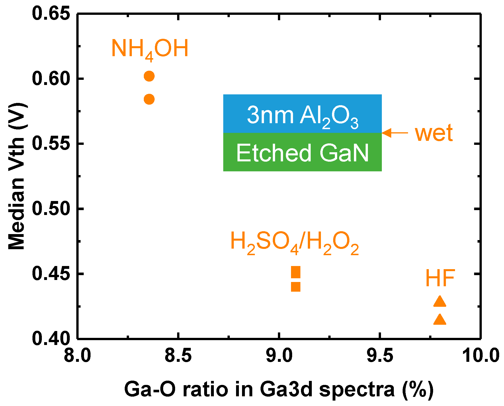
3.1. Interface
3.2. Dielectric
- Larger band gap than GaN in another to have a conduction offset higher than 1 eV;
- Layer without grain boundaries;
- High relative permittivity and high breakdown voltage.
3.2.1. Al2O3 and AlN Alloys for Improved Thermal Stability and Lower Electron Trapping: AlON
3.2.2. Al2O3 and SiO2 Alloys for Improved Thermal Stability and Lower Electron Trapping: AlSiO
3.2.3. HfO2 and SiO2 Alloys for Improved Mobility: HfSiOx
3.2.4. Al2O3 and TiO2 alloy for VTH Engineering: AlTiO
3.2.5. Summary
4. Conclusions
Author Contributions
Funding
Data Availability Statement
Conflicts of Interest
References
- Efthymiou, L.; Longobardi, G.; Camuso, G.; Chien, T.; Chen, M.; Udrea, F. On the Physical Operation and Optimization of the P-GaN Gate in Normally-off GaN HEMT Devices. Appl. Phys. Lett. 2017, 110, 123502. [Google Scholar] [CrossRef]
- Hu, Y.; Hernández-Gutiérrez, C.A.; Solís-Cisneros, H.I.; Santana, G.; Kudriatsev, Y.; Camas-Anzueto, J.L.; López-López, M. Blue Luminescence Origin and Mg Acceptor Saturation in Highly Doped Zinc-Blende GaN with Mg. J. Alloy. Compd. 2022, 897, 163133. [Google Scholar] [CrossRef]
- Lossy, R.; Gargouri, H.; Arens, M.; Würfl, J. Gallium Nitride MIS-HEMT Using Atomic Layer Deposited Al2O3 as Gate Dielectric. J. Vac. Sci. Technol. A Vac. Surf. Film. 2013, 31, 01A140. [Google Scholar] [CrossRef]
- Ahn, J.; Kim, D.; Park, K.-H.; Yoo, G.; Heo, J. Pt-Decorated Graphene Gate AlGaN/GaN MIS-HEMT for Ultrahigh Sensitive Hydrogen Gas Detection. IEEE Trans. Electron Devices 2021, 68, 1255–1261. [Google Scholar] [CrossRef]
- Texas Instrument. LMG1020 5-V, 7-A, 5-A Low-Side GaN and MOSFET Driver For 1-Ns Pulse Width Applications; Texas Instrument: Dallas, TX, USA, 2018; p. 26. [Google Scholar]
- Le Royer, C.; Mohamad, B.; Biscarrat, J.; Vauche, L.; Escoffier, R.; Buckley, J.; Bécu, S.; Riat, R.; Gillot, C.; Charles, M.; et al. Normally-OFF 650V GaN-on-Si MOSc-HEMT Transistor: Benefits of the Fully Recessed Gate Architecture. In Proceedings of the 2022 IEEE 34th International Symposium on Power Semiconductor Devices and ICs (ISPSD), Vancouver, BC, Canada, 22–25 May 2022; pp. 49–52. [Google Scholar]
- Zhu, R.; Jiang, H.; Tang, C.W.; Lau, K.M. High-Performance GaN Vertical Trench MOSFETs Grown on Si Substrate. In Proceedings of the 2022 Compound Semiconductor Week (CSW), Ann Arbor, MI, USA, 1–3 June 2022; pp. 1–2. [Google Scholar]
- Khadar, R.A.; Liu, C.; Soleimanzadeh, R.; Matioli, E. Fully Vertical GaN-on-Si Power MOSFETs. IEEE Electron Device Lett. 2019, 40, 443–446. [Google Scholar] [CrossRef]
- Amano, H.; Baines, Y.; Beam, E.; Borga, M.; Bouchet, T.; Chalker, P.R.; Charles, M.; Chen, K.J.; Chowdhury, N.; Chu, R.; et al. The 2018 GaN Power Electronics Roadmap. J. Phys. D Appl. Phys. 2018, 51, 163001. [Google Scholar] [CrossRef]
- He, J.; Cheng, W.-C.; Wang, Q.; Cheng, K.; Yu, H.; Chai, Y. Recent Advances in GaN-Based Power HEMT Devices. Adv. Electron. Mater. 2021, 7, 2001045. [Google Scholar] [CrossRef]
- Pearton, S.J.; Douglas, E.A.; Shul, R.J.; Ren, F. Plasma Etching of Wide Bandgap and Ultrawide Bandgap Semiconductors. J. Vac. Sci. Technol. A 2020, 38, 020802. [Google Scholar] [CrossRef] [Green Version]
- Sreenidhi, T.; Baskar, K.; DasGupta, A.; DasGupta, N. Reactive Ion Etching of GaN in SF6 + Ar and SF6 + N2 Plasma. Semicond. Sci. Technol. 2008, 23, 125019. [Google Scholar] [CrossRef]
- Shah, A.P.; Azizur Rahman, A.; Bhattacharya, A. Temperature-Dependence of Cl2/Ar ICP-RIE of Polar, Semipolar, and Nonpolar GaN and AlN Following BCl3/Ar Breakthrough Plasma. J. Vac. Sci. Technol. A 2020, 38, 013001. [Google Scholar] [CrossRef]
- Lai, Y.-H.; Yeh, C.-T.; Hwang, J.-M.; Hwang, H.-L.; Chen, C.-T.; Hung, W.-H. Sputtering and Etching of GaN Surfaces. J. Phys. Chem. B 2001, 105, 10029–10036. [Google Scholar] [CrossRef]
- Kambayashi, H.; Satoh, Y.; Ootomo, S.; Kokawa, T.; Nomura, T.; Kato, S.; Chow, T.P. Over 100A Operation Normally-off AlGaN/GaN Hybrid MOS-HFET on Si Substrate with High-Breakdown Voltage. Solid-State Electron. 2010, 54, 660–664. [Google Scholar] [CrossRef]
- Liu, Z.; Wang, Y.; Xia, X.; Yang, H.; Li, J.; Gu, C. Fabrication of GaN Hexagonal Cones by Inductively Coupled Plasma Reactive Ion Etching. J. Vac. Sci. Technol. B Nanotechnol. Microelectron. Mater. Process. Meas. Phenom. 2016, 34, 041226. [Google Scholar] [CrossRef]
- Constant, A.; Baele, J.; Coppens, P.; Pestel, F.D.; Moens, P.; Tack, M. Recessing Process for Au-Free Ohmic Contacts Formation on AlGaN/GaN Heterostructures with AlN Spacer. In Proceedings of the 2017 International Conference on Compound Semiconductor Manufacturing Technology (CS MANTECH), Indian Wells, CA, USA, 22–25 May 2017. [Google Scholar]
- Yamada, S.; Sakurai, H.; Osada, Y.; Furuta, K.; Nakamura, T.; Kamimura, R.; Narita, T.; Suda, J.; Kachi, T. Formation of Highly Vertical Trenches with Rounded Corners via Inductively Coupled Plasma Reactive Ion Etching for Vertical GaN Power Devices. Appl. Phys. Lett. 2021, 118, 102101. [Google Scholar] [CrossRef]
- Buttari, D.; Heikman, S.; Keller, S.; Mishra, U.K. Digital Etching for Highly Reproducible Low Damage Gate Recessing on AlGaN/GaN HEMTs. In Proceedings of the IEEE Lester Eastman Conference on High Performance Devices, Newark, DE, USA, 8 August 2002. [Google Scholar]
- Kanarik, K.J.; Lill, T.; Hudson, E.A.; Sriraman, S.; Tan, S.; Marks, J.; Vahedi, V.; Gottscho, R.A. Overview of Atomic Layer Etching in the Semiconductor Industry. J. Vac. Sci. Technol. A Vac. Surf. Film. 2015, 33, 020802. [Google Scholar] [CrossRef] [Green Version]
- Benrabah, S.; Legallais, M.; Besson, P.; Ruel, S.; Vauche, L.; Pelissier, B.; Thieuleux, C.; Salem, B.; Charles, M. H3PO4-Based Wet Chemical Etching for Recovery of Dry-Etched GaN Surfaces. Appl. Surf. Sci. 2022, 582, 152309. [Google Scholar] [CrossRef]
- Cao, X.A.; Cho, H.; Pearton, S.J.; Dang, G.T.; Zhang, A.P.; Ren, F.; Shul, R.J.; Zhang, L.; Hickman, R.; Van Hove, J.M. Depth and Thermal Stability of Dry Etch Damage in GaN Schottky Diodes. Appl. Phys. Lett. 1999, 75, 232–234. [Google Scholar] [CrossRef]
- Wang, Q.; Jiang, Y.; Zhang, J.; Kawaharada, K.; Li, L.; Wang, D.; Ao, J.-P. Effects of Recess Process and Surface Treatment on the Threshold Voltage of GaN MOSFETs Fabricated on a AlGaN/GaN Heterostructure. Semicond. Sci. Technol. 2015, 30, 065004. [Google Scholar] [CrossRef]
- Lee, J.-M.; Chang, K.-M.; Kim, S.-W.; Huh, C.; Lee, I.-H.; Park, S.-J. Dry Etch Damage in N-Type GaN and Its Recovery by Treatment with an N2 Plasma. J. Appl. Phys. 2000, 87, 5. [Google Scholar] [CrossRef] [Green Version]
- Yamada, S.; Takeda, K.; Toguchi, M.; Sakurai, H.; Nakamura, T.; Suda, J.; Kachi, T.; Sato, T. Depth Profiling of Surface Damage in N-Type GaN Induced by Inductively Coupled Plasma Reactive Ion Etching Using Photo-Electrochemical Techniques. Appl. Phys. Express 2020, 13, 106505. [Google Scholar] [CrossRef]
- Tokuda, H.; Harada, S.; Asubar, J.T.; Kuzuhara, M. Influence of Reactive-Ion-Etching Depth on Interface Properties in Al2O3/n-GaN MOS Diodes. Jpn. J. Appl. Phys. 2019, 58, 106503. [Google Scholar] [CrossRef]
- Jiang, Y.; Wang, Q.P.; Tamai, K.; Miyashita, T.; Motoyama, S.; Wang, D.J.; Ao, J.P.; Ohno, Y. GaN MOSFET with Boron Trichloride-Based Dry Recess Process. J. Phys. Conf. Ser. 2013, 441, 012025. [Google Scholar] [CrossRef] [Green Version]
- Yatabe, Z.; Asubar, J.T.; Hashizume, T. Insulated Gate and Surface Passivation Structures for GaN-Based Power Transistors. J. Phys. D Appl. Phys. 2016, 49, 393001. [Google Scholar] [CrossRef]
- Takashima, S.; Li, Z.; Chow, T.P. Sidewall Dominated Characteristics on Fin-Gate AlGaN/GaN MOS-Channel-HEMTs. IEEE Trans. Electron Devices 2013, 60, 3025–3031. [Google Scholar] [CrossRef]
- Yatabe, Z.; Hori, Y.; Kim, S.; Hashizume, T. Effects of Cl2-Based Inductively Coupled Plasma Etching of AlGaN on Interface Properties of Al2O3/AlGaN/GaN Heterostructures. Appl. Phys. Express 2013, 6, 016502. [Google Scholar] [CrossRef]
- Fukumizu, H.; Sekine, M.; Hori, M.; Kanomaru, K.; Kikuchi, T. Atomic Layer Etching of AlGaN Using Cl2 and Ar Gas Chemistry and UV Damage Evaluation. J. Vac. Sci. Technol. A 2019, 37, 021002. [Google Scholar] [CrossRef]
- Foster, G.M.; Koehler, A.; Ebrish, M.; Gallagher, J.; Anderson, T.; Noesges, B.; Brillson, L.; Gunning, B.; Hobart, K.D.; Kub, F. Recovery from Plasma Etching-Induced Nitrogen Vacancies in p-Type Gallium Nitride Using UV/O3 Treatments. Appl. Phys. Lett. 2020, 117, 082103. [Google Scholar] [CrossRef]
- Pernel, C.; Berthou, W.; Suman, S.; Ruel, S.; Vauche, L. Electrochemical Short Loop to Assess the Impact of Plasma and Surface Treatments on N-GaN. In Proceedings of the 2022 International Workshop on Nitrides Semiconductors, Berlin, Germany, 9–14 October 2022. [Google Scholar]
- Lehmann, J.; Leroux, C.; Reimbold, G.; Charles, M.; Torres, A.; Morvan, E.; Baines, Y.; Ghibaudo, G.; Bano, E. Novel Sheet Resistance Measurement on AlGaN/GaN HEMT Wafer Adapted from Four-Point Probe Technique. In Proceedings of the Proceedings of the 2015 International Conference on Microelectronic Test Structures, Tempe, AZ, USA, 23–26 March 2015; pp. 163–168. [Google Scholar]
- Pimenta-Barros, P.; Chauvet, N.; Roux, F.L.; Burtin, P.; Tan, S.; Barnola, S.; Ruel, S.; Vauche, L.; Torres, A.; Plissonnier, M.; et al. GaN Damage Evaluation after Conventional Plasma Etching and Anisotropic Atomic Layer Etching. In Proceedings of the 41st International Symposium on Dry Process (DPS2019), Hiroshima, Japan, 21–22 November 2019; Volume 41, pp. 43–44. [Google Scholar]
- Ruel, S.; Pimenta-Barros, P.; Roux, F.L.; Chauvet, N.; Massardier, M.; Thoueille, P.; Tan, S.; Shin, D.; Gaucher, F.; Posseme, N. Atomic Layer Etching of GaN Using Cl2 and He or Ar Plasma. J. Vac. Sci. Technol. A 2021, 39, 022601. [Google Scholar] [CrossRef]
- Tang, K.; Huang, W.; Chow, T.P. GaN MOS Capacitors and FETs on Plasma-Etched GaN Surfaces. J. Electron. Mater. 2009, 38, 523–528. [Google Scholar] [CrossRef]
- Cao, X.A.; Pearton, S.J.; Zhang, A.P.; Dang, G.T.; Ren, F.; Shul, R.J.; Zhang, L.; Hickman, R.; Hove, J.M.V. Electrical Effects of Plasma Damage in P-GaN. Appl. Phys. Lett. 1999, 75, 4. [Google Scholar] [CrossRef]
- Lin, M.E.; Fan, Z.F.; Ma, Z.; Allen, L.H.; Morkoç, H. Reactive Ion Etching of GaN Using BCl3. Appl. Phys. Lett. 1994, 64, 887–888. [Google Scholar] [CrossRef]
- Sato, T.; Toguchi, M.; Komatsu, Y.; Uemura, K. Low-Damage Etching for AlGaN/GaN HEMTs Using Photo-Electrochemical Reactions. IEEE Trans. Semicond. Manuf. 2019, 32, 483–488. [Google Scholar] [CrossRef] [Green Version]
- Heffernan, C.; Lynch, R.P.; Buckley, D.N. A Study of the Photoelectrochemical Etching of N-GaN in H3PO4 and KOH Electrolytes. ECS J. Solid State Sci. Technol. 2020, 9, 015003. [Google Scholar] [CrossRef] [Green Version]
- Fariza, A.; Ji, X.; Gao, Y.; Ran, J.; Wang, J.; Wei, T. Role of Energy-Band Offset in Photo-Electrochemical Etching Mechanism of p-GaN Heterostructures. J. Appl. Phys. 2021, 129, 165701. [Google Scholar] [CrossRef]
- Horikiri, F.; Ohta, H.; Asai, N.; Narita, Y.; Yoshida, T.; Mishima, T. Excellent Potential of Photo-Electrochemical Etching for Fabricating High-Aspect-Ratio Deep Trenches in Gallium Nitride. Appl. Phys. Express 2018, 11, 091001. [Google Scholar] [CrossRef]
- Thayne, I.; Li, X.; Millar, D.; Fu, Y.-C.; Peralagu, U. Plasma Processing of III-V Materials for Energy Efficient Electronics Applications; Engelmann, S.U., Wise, R.S., Engelmann, S.U., Wise, R.S., Eds.; SPIE: San Jose, CA, USA, 2017; p. 101490R. [Google Scholar]
- Yamada, S. Reduction of Plasma-Induced Damage in n-Type GaN by Multistep-Bias Etching in Inductively Coupled Plasma Reactive Ion Etching. Appl. Phys. Express 2019, 13, 016505. [Google Scholar] [CrossRef]
- Lin, Y.-K.; Noda, S.; Lo, H.-C.; Liu, S.-C.; Wu, C.-H.; Wong, Y.-Y.; Luc, Q.H.; Chang, P.-C.; Hsu, H.-T.; Samukawa, S.; et al. AlGaN/GaN HEMTs With Damage-Free Neutral Beam Etched Gate Recess for High-Performance Millimeter-Wave Applications. IEEE Electron Device Lett. 2016, 37, 1395–1398. [Google Scholar] [CrossRef]
- Kauppinen, C.; Khan, S.A.; Sundqvist, J.; Suyatin, D.B.; Suihkonen, S.; Kauppinen, E.I.; Sopanen, M. Atomic Layer Etching of Gallium Nitride (0001). J. Vac. Sci. Technol. A Vac. Surf. Film. 2017, 35, 060603. [Google Scholar] [CrossRef] [Green Version]
- Ohba, T.; Yang, W.; Tan, S.; Kanarik, K.J.; Nojiri, K. Atomic Layer Etching of GaN and AlGaN Using Directional Plasma-Enhanced Approach. Jpn. J. Appl. Phys. 2017, 56, 06HB06. [Google Scholar] [CrossRef] [Green Version]
- Kanarik, K.J.; Tan, S.; Yang, W.; Kim, T.; Lill, T.; Kabansky, A.; Hudson, E.A.; Ohba, T.; Nojiri, K.; Yu, J.; et al. Predicting Synergy in Atomic Layer Etching. J. Vac. Sci. Technol. A Vac. Surf. Film. 2017, 35, 05C302. [Google Scholar] [CrossRef] [Green Version]
- Aroulanda, S.; Patard, O.; Altuntas, P.; Michel, N.; Pereira, J.; Lacam, C.; Gamarra, P.; Delage, S.L.; Defrance, N.; de Jaeger, J.-C.; et al. Cl2/Ar Based Atomic Layer Etching of AlGaN Layers. J. Vac. Sci. Technol. A 2019, 37, 041001. [Google Scholar] [CrossRef]
- Despiau-Pujo, E.; Chabert, P.; Bansropun, S.; Thénot, D.; Plouhinec, P.; Cassette, S. Simulations of Radical and Ion Fluxes on a Wafer in a Cl2/Ar Inductively Coupled Plasma Discharge: Confrontation with GaAs and GaN Etch Experiments. J. Vac. Sci. Technol. B Nanotechnol. Microelectron. Mater. Process. Meas. Phenom. 2010, 28, 693–701. [Google Scholar] [CrossRef]
- Despiau-Pujo, E.; Chabert, P. MD Simulations of GaN Sputtering by Ar+ Ions: Ion-Induced Damage and near-Surface Modification under Continuous Bombardment. J. Vac. Sci. Technol. A Vac. Surf. Film. 2010, 28, 1105–1110. [Google Scholar] [CrossRef]
- Deenapanray, P.N.K.; Petravić, M.; Kim, K.-J.; Kim, B.; Li, G. Compositional Changes on GaN Surfaces under Low-Energy Ion Bombardment Studied by Synchrotron-Based Spectroscopies. Appl. Phys. Lett. 2003, 83, 4948–4950. [Google Scholar] [CrossRef] [Green Version]
- Petravic, M.; Deenapanray, P.N.K.; Coleman, V.A.; Kim, K.; Kim, B.; Li, G. Core-Level Photoemission and near-Edge x-Ray Absorption Fine-Structure Studies of GaN Surface under Low-Energy Ion Bombardment. J. Appl. Phys. 2004, 95, 5487–5493. [Google Scholar] [CrossRef] [Green Version]
- Venugopal, V.; Upadhyaya, K.; Kumar, K.; Shivaprasad, S.M. Ion Induced Compositional Changes and Nanodroplet Formation on GaN Surface. Appl. Surf. Sci. 2014, 315, 440–444. [Google Scholar] [CrossRef]
- Petravic, M.; Coleman, V.A.; Kim, K.-J.; Kim, B.; Li, G. Defect Acceptor and Donor in Ion-Bombarded GaN. J. Vac. Sci. Technol. A Vac. Surf. Film. 2005, 23, 1340–1345. [Google Scholar] [CrossRef] [Green Version]
- Hua, M.; Liu, C.; Yang, S.; Liu, S.; Fu, K.; Dong, Z.; Cai, Y.; Zhang, B.; Chen, K.J. GaN-Based Metal-Insulator-Semiconductor High-Electron-Mobility Transistors Using Low-Pressure Chemical Vapor Deposition SiNx as Gate Dielectric. IEEE Electron Device Lett. 2015, 36, 448–450. [Google Scholar] [CrossRef]
- Hua, M.; Zhang, Z.; Qian, Q.; Wei, J.; Bao, Q.; Tang, G.; Chen, K.J. High-Performance Fully-Recessed Enhancement- Mode GaN MIS-FETs with Crystalline Oxide Interlayer. In Proceedings of the 29th International Symposium on Power Semiconductor Devices & ICs, Sapporo, Japan, 28 May–1 June 2017. [Google Scholar]
- Hua, M.; Zhang, Z.; Wei, J.; Lei, J.; Tang, G.; Fu, K.; Cai, Y.; Zhang, B.; Chen, K.J. Integration of LPCVD-SiNx Gate Dielectric with Recessed-Gate E-Mode GaN MIS-FETs: Toward High Performance, High Stability and Long TDDB Lifetime. In Proceedings of the 2016 IEEE International Electron Devices Meeting (IEDM), San Francisco, CA, USA, 3–7 December 2016. [Google Scholar]
- Le Roux, F.; Possémé, N.; Burtin, P.; Barnola, S.; Torres, A. XPS Study of a Selective GaN Etching Process Using Self-Limiting Cyclic Approach for Power Devices Application. Microelectron. Eng. 2020, 228, 111328. [Google Scholar] [CrossRef]
- Zhou, Q.; Zhang, A.; Zhu, R.; Shi, Y.; Wang, Z.; Liu, L.; Chen, B.; Jin, Y.; Chen, W.; Zhang, B. Threshold Voltage Modulation by Interface Charge Engineering for High Performance Normally-off GaN MOSFETs with High Faulty Turn-on Immunity. In Proceedings of the 2016 28th International Symposium on Power Semiconductor Devices and ICs (ISPSD), Prague, Czech Republic, 12–16 June 2016. [Google Scholar]
- Wu, J.; Lei, S.; Cheng, W.-C.; Sokolovskij, R.; Wang, Q.; Xia, G. (Maggie); Yu, H. Oxygen-Based Digital Etching of AlGaN/GaN Structures with AlN as Etch-Stop Layers. J. Vac. Sci. Technol. A 2019, 37, 060401. [Google Scholar] [CrossRef] [Green Version]
- Zhu, J.; Jing, S.; Ma, X.; Liu, S.; Wang, P.; Zhang, Y.; Zhu, Q.; Mi, M.; Hou, B.; Yang, L.; et al. Improvement of Electron Transport Property and On-Resistance in Normally-OFF Al2O3/AlGaN/GaN MOS-HEMTs Using Post-Etch Surface Treatment. IEEE Trans. Electron Devices 2020, 67, 3541–3547. [Google Scholar] [CrossRef]
- Chiu, H.-C.; Chang, Y.-S.; Li, B.-H.; Wang, H.-C.; Kao, H.-L.; Chien, F.-T.; Hu, C.-W.; Xuan, R. High Uniformity Normally-OFF p-GaN Gate HEMT Using Self-Terminated Digital Etching Technique. IEEE Trans. Electron Devices 2018, 65, 4820–4825. [Google Scholar] [CrossRef]
- Shih, P.-C.; Engel, Z.; Ahmad, H.; Doolittle, W.A.; Palacios, T. Wet-Based Digital Etching on GaN and AlGaN. Appl. Phys. Lett. 2022, 120, 022101. [Google Scholar] [CrossRef]
- Zhou, Q.; Chen, B.; Jin, Y.; Huang, S.; Wei, K.; Liu, X.; Bao, X.; Mou, J.; Zhang, B. High-Performance Enhancement-Mode Al2O3/AlGaN/GaN-on-Si MISFETs With 626 MW/Cm2 Figure of Merit. IEEE Trans. Electron Devices 2015, 62, 776–781. [Google Scholar] [CrossRef]
- Burnham, S.D.; Boutros, K.; Hashimoto, P.; Butler, C.; Wong, D.W.S.; Hu, M.; Micovic, M. Gate-Recessed Normally-off GaN-on- Si HEMT Using a New O2-BCl3 Digital Etching Technique. Phys. Status Solidi (C) 2010, 7, 2010–2012. [Google Scholar] [CrossRef]
- Mikhailovich, S.V.; Pavlov, A.Y.; Tomosh, K.N.; Fedorov, Y.V. Low-Energy Defectless Dry Etching of the AlGaN/AlN/GaN HEMT Barrier Layer. Tech. Phys. Lett. 2018, 44, 435–437. [Google Scholar] [CrossRef]
- Hu, Q.; Li, S.; Li, T.; Wang, X.; Li, X.; Wu, Y. Channel Engineering of Normally-OFF AlGaN/GaN MOS-HEMTs by Atomic Layer Etching and High-κ Dielectric. IEEE Electron Device Lett. 2018, 39, 1377–1380. [Google Scholar] [CrossRef]
- Zhou, Q.; Yang, Y.; Hu, K.; Zhu, R.; Chen, W.; Zhang, B. Device Technologies of GaN-on-Si for Power Electronics: Enhancement-Mode Hybrid MOS-HFET and Lateral Diode. IEEE Trans. Ind. Electron. 2017, 64, 8971–8979. [Google Scholar] [CrossRef]
- Wang, H.; Wang, J.; Li, M.; Cao, Q.; Yu, M.; He, Y.; Wu, W. 823-MA/Mm Drain Current Density and 945-MW/Cm2 Baliga’s Figure-of-Merit Enhancement-Mode GaN MISFETs With a Novel PEALD-AlN/LPCVD-Si3N4 Dual-Gate Dielectric. IEEE Electron Device Lett. 2018, 39, 1888–1891. [Google Scholar] [CrossRef]
- Gao, J.; Jin, Y.; Xie, B.; Wen, C.P.; Hao, Y.; Wang, M. GaN Lateral Schottky Diodes with High Baliga’s Figure-of-Merit Utilizing Self-Terminated, Low Damage Anode Recessing Technology. In Proceedings of the 2018 76th Device Research Conference (DRC), Santa Barbara, CA, USA, 24–27 June 2018; pp. 1–2. [Google Scholar]
- Lin, S.; Wang, M.; Sang, F.; Tao, M.; Wen, C.P.; Xie, B.; Yu, M.; Wang, J.; Hao, Y.; Wu, W.; et al. A GaN HEMT Structure Allowing Self-Terminated, Plasma-Free Etching for High-Uniformity, High-Mobility Enhancement-Mode Devices. IEEE Electron Device Lett. 2016, 37, 377–380. [Google Scholar] [CrossRef]
- Tao, M.; Liu, S.; Xie, B.; Wen, C.P.; Wang, J.; Hao, Y.; Wu, W.; Cheng, K.; Shen, B.; Wang, M. Characterization of 880 V Normally Off GaN MOSHEMT on Silicon Substrate Fabricated With a Plasma-Free, Self-Terminated Gate Recess Process. IEEE Trans. Electron Devices 2018, 65, 1453–1457. [Google Scholar] [CrossRef]
- Jo, Y.-W.; Son, D.-H.; Won, C.-H.; Lee, J.-H. Normally-Off AlGaN/GaN-Based MOSHEMT by Using One-Step TMAH Wet Etching. Korean Soc. Electron. Eng. Conf. 2016, 11, 945–949. [Google Scholar]
- Eller, B.S.; Yang, J.; Nemanich, R.J. Electronic Surface and Dielectric Interface States on GaN and AlGaN. J. Vac. Sci. Technol. A Vac. Surf. Film. 2013, 31, 050807. [Google Scholar] [CrossRef]
- Zywietz, T.K.; Neugebauer, J.; Scheffler, M. The Adsorption of Oxygen at GaN Surfaces. Appl. Phys. Lett. 1999, 74, 1695–1697. [Google Scholar] [CrossRef] [Green Version]
- Khadar, R.A.; Liu, C.; Soleimanzadeh1=, R.; Matioli, E. Fully-Vertical GaN-on-Si Power MOSFETs. In Proceedings of the 2018 IEEE International Electron Devices Meeting (IEDM), Francisco, CA, USA, 1–5 December 2018; pp. 1–2. [Google Scholar]
- Hirai, H.; Miura, Y.; Nakajima, A.; Harada, S.; Yamaguchi, H. Crystal-Orientation-Dependent Flatband Voltage of Non-Polar GaN MOS Interfaces Investigated Using Trench Sidewall Capacitors. Appl. Phys. Lett. 2021, 119, 071601. [Google Scholar] [CrossRef]
- Kodama, M.; Sugimoto, M.; Hayashi, E.; Soejima, N.; Ishiguro, O.; Kanechika, M.; Itoh, K.; Ueda, H.; Uesugi, T.; Kachi, T. GaN-Based Trench Gate Metal Oxide Semiconductor Field-Effect Transistor Fabricated with Novel Wet Etching. Appl. Phys. Express 2008, 1, 021104. [Google Scholar] [CrossRef]
- Ji, D.; Li, W.; Agarwal, A.; Chan, S.H.; Haller, J.; Bisi, D.; Labrecque, M.; Gupta, C.; Cruse, B.; Lal, R.; et al. Improved Dynamic RON of GaN Vertical Trench MOSFETs (OG-FETs) Using TMAH Wet Etch. IEEE Electron Device Lett. 2018, 39, 1030–1033. [Google Scholar] [CrossRef]
- Lu, B.; Sun, M.; Palacios, T. An Etch-Stop Barrier Structure for GaN High-Electron-Mobility Transistors. IEEE Electron Device Lett. 2013, 34, 369–371. [Google Scholar] [CrossRef]
- Im, K.-S. Mobility Fluctuations in a Normally-Off GaN MOSFET Using Tetramethylammonium Hydroxide Wet Etching. IEEE Electron Device Lett. 2021, 42, 18–21. [Google Scholar] [CrossRef]
- Reddy, M.S.P.; Park, W.-S.; Im, K.-S.; Lee, J.-H. Dual-Surface Modification of AlGaN/GaN HEMTs Using TMAH and Piranha Solutions for Enhancing Current and 1/f-Noise Characteristics. IEEE J. Electron Devices Soc. 2018, 6, 791–796. [Google Scholar] [CrossRef]
- Stocker, D.A.; Schubert, E.F.; Redwing, J.M. Crystallographic Wet Chemical Etching of GaN. Appl. Phys. Lett. 1998, 73, 2654–2656. [Google Scholar] [CrossRef] [Green Version]
- Wong, M.S.; Lee, C.; Myers, D.J.; Hwang, D.; Kearns, J.A.; Li, T.; Speck, J.S.; Nakamura, S.; DenBaars, S.P. Size-Independent Peak Efficiency of III-Nitride Micro-Light-Emitting-Diodes Using Chemical Treatment and Sidewall Passivation. Appl. Phys. Express 2019, 12, 097004. [Google Scholar] [CrossRef]
- Yang, J.; Eller, B.S.; Nemanich, R.J. Surface Band Bending and Band Alignment of Plasma Enhanced Atomic Layer Deposited Dielectrics on Ga- and N-Face Gallium Nitride. J. Appl. Phys. 2014, 116, 123702. [Google Scholar] [CrossRef] [Green Version]
- Meunier, R.; Torres, A.; Charles, M.; Morvan, E.; Petit-Etienne, C.; Renault, O.; Billon, T. XPS Analysis of AlGaN/GaN Surface after Chemical and N-Containing Plasma Treatments. ECS Trans. 2012, 50, 451–460. [Google Scholar] [CrossRef]
- Sohal, R.; Dudek, P.; Hilt, O. Comparative Study of NH4OH and HCl Etching Behaviours on AlGaN Surfaces. Appl. Surf. Sci. 2010, 256, 2210–2214. [Google Scholar] [CrossRef]
- Zhernokletov, D.M.; Negara, M.A.; Long, R.D.; Aloni, S.; Nordlund, D.; McIntyre, P.C. Interface Trap Density Reduction for Al2O3/GaN (0001) Interfaces by Oxidizing Surface Preparation Prior to Atomic Layer Deposition. ACS Appl. Mater. Interfaces 2015, 7, 12774–12780. [Google Scholar] [CrossRef]
- Vauche, L.; Chanuel, A.; Martinez, E.; Roure, M.-C.; Le Royer, C.; Bécu, S.; Gwoziecki, R.; Plissonnier, M. Study of an Al2O3/GaN Interface for Normally Off MOS-Channel High-Electron-Mobility Transistors Using XPS Characterization: The Impact of Wet Surface Treatment on Threshold Voltage VTH. ACS Appl. Electron. Mater. 2021, 3, 1170–1177. [Google Scholar] [CrossRef]
- Jackson, C.M.; Arehart, A.R.; Grassman, T.J.; McSkimming, B.; Speck, J.S.; Ringel, S.A. Impact of Surface Treatment on Interface States of ALD Al2O3/GaN Interfaces. ECS J. Solid State Sci. Technol. 2017, 6, P489–P494. [Google Scholar] [CrossRef]
- King, S.W.; Barnak, J.P.; Bremser, M.D.; Tracy, K.M.; Ronning, C.; Davis, R.F.; Nemanich, R.J. Cleaning of AlN and GaN Surfaces. J. Appl. Phys. 1998, 84, 5248–5260. [Google Scholar] [CrossRef]
- Uhlrich, J.J.; Grabow, L.C.; Mavrikakis, M.; Kuech, T.F. Practical Surface Treatments and Surface Chemistry of N-Type and p-Type GaN. J. Electron. Mater. 2008, 37, 439–447. [Google Scholar] [CrossRef]
- Okada, H.; Shinohara, M.; Kondo, Y.; Sekiguchi, H.; Yamane, K.; Wakahara, A. Investigation of HCl-Based Surface Treatment for GaN Devices. AIP Conf. Proc. 2016, 1709, 020011. [Google Scholar]
- Rosenberg, S.G.; Pennachio, D.J.; Wagenbach, C.; Johnson, S.D.; Nepal, N.; Kozen, A.C.; Woodward, J.M.; Robinson, Z.; Joress, H.; Ludwig, K.F.; et al. Low Temperature Surface Preparation of GaN Substrates for Atomic Layer Epitaxial Growth: Assessment of Ex Situ Preparations. J. Vac. Sci. Technol. A 2019, 37, 020908. [Google Scholar] [CrossRef]
- English, C.R.; Wheeler, V.D.; Garces, N.Y.; Nepal, N.; Nath, A.; Hite, J.K.; Mastro, M.A.; Eddy, C.R. Impact of Surface Treatments on High-κ Dielectric Integration with Ga-Polar and N-Polar GaN. J. Vac. Sci. Technol. B Nanotechnol. Microelectron. Mater. Process. Meas. Phenom. 2014, 32, 03D106. [Google Scholar] [CrossRef]
- Yamamoto, A.; Kanatani, K.; Makino, S.; Kuzuhara, M. Metalorganic Vapor Phase Epitaxial Growth of AlGaN Directly on Reactive-Ion Etching-Treated GaN Surfaces to Prepare AlGaN/GaN Heterostructures with High Electron Mobility (∼1500 Cm2V−1s−1): Impacts of Reactive-Ion Etching-Damaged Layer Removal. Jpn. J. Appl. Phys. 2018, 57, 125501. [Google Scholar] [CrossRef]
- Auzelle, T.; Ullrich, F.; Hietzschold, S.; Brackmann, S.; Hillebrandt, S.; Kowalsky, W.; Mankel, E.; Lovrincic, R.; Fernández-Garrido, S. Electronic Properties of Air-Exposed GaN(11-00) and (0001) Surfaces after Several Device Processing Compatible Cleaning Steps. Appl. Surf. Sci. 2019, 495, 143514. [Google Scholar] [CrossRef]
- Nepal, N.; Garces, N.Y.; Meyer, D.J.; Hite, J.K.; Mastro, M.A.; Eddy, C.R., Jr. Assessment of GaN Surface Pretreatment for Atomic Layer Deposited High- k Dielectrics. Appl. Phys. Express 2011, 4, 055802. [Google Scholar] [CrossRef]
- Duan, T.L.; Pan, J.S.; Ang, D.S. Investigation of Surface Band Bending of Ga-Face GaN by Angle-Resolved X-Ray Photoelectron Spectroscopy. ECS J. Solid State Sci. Technol. 2016, 5, P514–P517. [Google Scholar] [CrossRef]
- Hossain, T.; Wei, D.; Edgar, J.H.; Garces, N.Y.; Nepal, N.; Hite, J.K.; Mastro, M.A.; Eddy, C.R.; Meyer, H.M. Effect of GaN Surface Treatment on Al2O3/n-GaN MOS Capacitors. J. Vac. Sci. Technol. B Nanotechnol. Microelectron. Mater. Process. Meas. Phenom. 2015, 33, 061201. [Google Scholar] [CrossRef] [Green Version]
- Reiner, M.; Reiss, M.; Brünig, T.; Knuuttila, L.; Pietschnig, R.; Ostermaier, C. Chemical Understanding and Utility of H3PO4 Etching of Group-III- Nitrides: Chemical Understanding and Utility of H3PO4 Etching of Group-III-Nitrides. Phys. Status Solidi B 2015, 252, 1121–1126. [Google Scholar] [CrossRef]
- Lim, D.; Jung, W.S.; Choi, M.S.; Gil, Y.; Choi, C. The Effects of (NH4)2Sx Treatment on n-GaN MOS Device with Nano-Laminated ALD HfAlOx and Ru Gate Stack. Microelectron. Eng. 2015, 147, 210–214. [Google Scholar] [CrossRef]
- Han, H.H.; Lim, D.; Sergeevich, A.S.; Jeon, Y.-R.; Lee, J.H.; Son, S.K.; Choi, C. Suppressed Charge Trapping Characteristics of (NH4)2Sx Passivated GaN MOS Device with Atomic Layer Deposited HfAlOx Gate Dielectric. Microelectron. Eng. 2017, 178, 240–244. [Google Scholar] [CrossRef]
- Kim, K.; Jang, J. Improving Ni/GaN Schottky Diode Performance through Interfacial Passivation Layer Formed via Ultraviolet/Ozone Treatment. Curr. Appl. Phys. 2020, 20, 293–297. [Google Scholar] [CrossRef]
- Kim, K.; Ryu, J.H.; Kim, J.; Cho, S.J.; Liu, D.; Park, J.; Lee, I.-K.; Moody, B.; Zhou, W.; Albrecht, J.; et al. Band-Bending of Ga-Polar GaN Interfaced with Al2O3 through Ultraviolet/Ozone Treatment. ACS Appl. Mater. Interfaces 2017, 9, 17576–17585. [Google Scholar] [CrossRef] [PubMed]
- Li, Y.; Xiu, X.; Xiong, Z.; Hua, X.; Xie, Z.; Chen, P.; Liu, B.; Tao, T.; Zhang, R.; Zheng, Y. Single-Crystal GaN Layer Converted from β-Ga2O3Films and Its Application for Free-Standing GaN. CrystEngComm 2019, 21, 1224–1230. [Google Scholar] [CrossRef]
- Chen, D.-Y.; Persson, A.R.; Wen, K.-H.; Sommer, D.; Grünenpütt, J.; Blanck, H.; Thorsell, M.; Kordina, O.; Darakchieva, V.; Persson, P.O.Å.; et al. Impact of in Situ NH3 Pre-Treatment of LPCVD SiN Passivation on GaN HEMT Performance. Semicond. Sci. Technol. 2022, 37, 035011. [Google Scholar] [CrossRef]
- Ho, Y.J.; Jin, H.S.; Ha, M.-W.; Park, T.J. Sulfur Incorporation at Interface Between Atomic-Layer-Deposited Al2O3 Thin Film and AlGaN/GaN Heterostructure. Electron. Mater. Lett. 2019, 15, 179–185. [Google Scholar]
- Cho, S.J.; Roberts, J.W.; Guiney, I.; Li, X.; Ternent, G.; Floros, K.; Humphreys, C.J.; Chalker, P.R.; Thayne, I.G. A Study of the Impact of In-Situ Argon Plasma Treatment before Atomic Layer Deposition of Al2O3 on GaN Based Metal Oxide Semiconductor Capacitor. Microelectron. Eng. 2015, 147, 277–280. [Google Scholar] [CrossRef]
- Wu, X.; Luo, W.; Liu, L.; Guo, L.; Liang, R.; Xu, J.; Wang, J. Effects of Argon Plasma Pretreatment on Polar and Nonpolar GaN/Al2O3 Interface. In Proceedings of the 2016 5th International Symposium on Next-Generation Electronics (ISNE), Hsinchu, Taiwan, 4–6 May 2016; pp. 1–2. [Google Scholar]
- Jung, W.S.; Lim, D.; Han, H.; Sokolov, A.S.; Jeon, Y.-R.; Choi, C. Influence of In-Situ NH3 Plasma Passivation on the Electrical Characteristics of Ga-Face n-GaN MOS Capacitor with Atomic Layer Deposited HfO2. Solid-State Electron. 2018, 149, 52–56. [Google Scholar] [CrossRef]
- Chen, P.-Y.; Posadas, A.B.; Kwon, S.; Wang, Q.; Kim, M.J.; Demkov, A.A.; Ekerdt, J.G. Cubic Crystalline Erbium Oxide Growth on GaN(0001) by Atomic Layer Deposition. J. Appl. Phys. 2017, 122, 215302. [Google Scholar] [CrossRef]
- Qin, X.; Dong, H.; Brennan, B.; Azacatl, A.; Kim, J.; Wallace, R.M. Impact of N2 and Forming Gas Plasma Exposure on the Growth and Interfacial Characteristics of Al2O3 on AlGaN. Appl. Phys. Lett. 2013, 103, 221604. [Google Scholar] [CrossRef]
- Hashizume, T.; Ootomo, S.; Inagaki, T.; Hasegawa, H. Surface Passivation of GaN and GaN/AlGaN Heterostructures by Dielectric Films and Its Application to Insulated-Gate Heterostructure Transistors. J. Vac. Sci. Technol. B Microelectron. Nanometer Struct. 2003, 21, 1828. [Google Scholar] [CrossRef] [Green Version]
- Yang, S.; Tang, Z.; Wong, K.-Y.; Lin, Y.-S.; Liu, C.; Lu, Y.; Huang, S.; Chen, K.J. High-Quality Interface in Al2O3/GaN/GaN/AlGaN/GaN MIS Structures With In Situ Pre-Gate Plasma Nitridation. IEEE Electron Device Lett. 2013, 34, 1497–1499. [Google Scholar] [CrossRef]
- Ozaki, S.; Ohki, T.; Kanamura, M.; Imada, T.; Nakamura, N.; Okamoto, N.; Miyajima, T.; Kikkawa, T. Effect of Oxidant Source on Threshold Voltage Shift of AlGaN/GaN MIS-HEMTs Using ALD-Al2O3 Gate Insulator Films. In Proceedings of the 2012 International Conference on Compound Semiconductor Manufacturing Technology, CS MANTECH 2012, Boston, MA, USA, 23–26 April 2012. [Google Scholar]
- Liu, S.; Yang, S.; Tang, Z.; Jiang, Q.; Liu, C.; Wang, M.; Shen, B.; Chen, K.J. Interface/Border Trap Characterization of Al2O3/AlN/GaN Metal-Oxide-Semiconductor Structures with an AlN Interfacial Layer. Appl. Phys. Lett. 2015, 106, 051605. [Google Scholar] [CrossRef]
- Zhang, Z.; Li, W.; Fu, K.; Yu, G.; Zhang, X.; Zhao, Y.; Sun, S.; Song, L.; Deng, X.; Xing, Z.; et al. AlGaN/GaN MIS-HEMTs of Very-Low Vth Hysteresis and Current Collapse with In-Situ Pre-Deposition Plasma Nitridation and LPCVD-Si3N4 Gate Insulator. IEEE Electron Device Lett. 2017, 38, 236–239. [Google Scholar] [CrossRef]
- Yang, S.; Tang, Z.; Wong, K.-Y.; Lin, Y.-S.; Lu, Y.; Huang, S.; Chen, K.J. Mapping of Interface Traps in High-Performance Al2O3/AlGaN/GaN MIS-Heterostructures Using Frequency- and Temperature-Dependent C-V Techniques. In Proceedings of the Electron Devices Meeting (IEDM), 2013 IEEE International, Washington, DC, USA, 9–11 December 2013. [Google Scholar]
- Yang, S.; Liu, S.; Liu, C.; Hua, M.; Chen, K.J. Gate Stack Engineering for GaN Lateral Power Transistors. Semicond. Sci. Technol. 2016, 31, 024001. [Google Scholar] [CrossRef]
- Tzou, A.-J.; Chu, K.-H.; Lin, I.-F.; Østreng, E.; Fang, Y.-S.; Wu, X.-P.; Wu, B.-W.; Shen, C.-H.; Shieh, J.-M.; Yeh, W.-K.; et al. AlN Surface Passivation of GaN-Based High Electron Mobility Transistors by Plasma-Enhanced Atomic Layer Deposition. Nanoscale Res. Lett. 2017, 12, 315. [Google Scholar] [CrossRef] [Green Version]
- Guo, F.; Huang, S.; Wang, X.; Luan, T.; Shi, W.; Deng, K.; Fan, J.; Yin, H.; Shi, J.; Mu, F.; et al. Suppression of Interface States between Nitride-Based Gate Dielectrics and Ultrathin-Barrier AlGaN/GaN Heterostructure with in Situ Remote Plasma Pretreatments. Appl. Phys. Lett. 2021, 118, 093503. [Google Scholar] [CrossRef]
- Amalraj, F.W.; Dhasiyan, A.K.; Lu, Y.; Shimizu, N.; Oda, O.; Ishikawa, K.; Kondo, H.; Sekine, M.; Ikarashi, N.; Hori, M. Effect of N2/H2 Plasma on GaN Substrate Cleaning for Homoepitaxial GaN Growth by Radical-Enhanced Metalorganic Chemical Vapor Deposition (REMOCVD). AIP Adv. 2018, 8, 115116. [Google Scholar] [CrossRef] [Green Version]
- Horng, R.-H.; Tseng, M.-C.; Wuu, D.-S. Surface Treatments on the Characteristics of Metal–Oxide Semiconductor Capacitors. Crystals 2019, 9, 1. [Google Scholar] [CrossRef] [Green Version]
- Mukherjee, K.; De Santi, C.; You, S.; Geens, K.; Borga, M.; Decoutere, S.; Bakeroot, B.; Diehle, P.; Altmann, F.; Meneghesso, G.; et al. Study and Characterization of GaN MOS Capacitors: Planar vs Trench Topographies. Appl. Phys. Lett. 2022, 120, 143501. [Google Scholar] [CrossRef]
- Yang, C.; Luo, X.; Zhang, A.; Deng, S.; Ouyang, D.; Peng, F.; Wei, J.; Zhang, B.; Li, Z. AlGaN/GaN MIS-HEMT With AlN Interface Protection Layer and Trench Termination Structure. IEEE Trans. Electron Devices 2018, 65, 5203–5207. [Google Scholar] [CrossRef]
- Wei, D.; Hossain, T.; Nepal, N.; Garces, N.Y.; Hite, J.K.; Meyer, H.M.; Eddy, C.R.; Edgar, J.H. Comparison of the Physical, Chemical and Electrical Properties of ALD Al2O3 on c- and m- Plane GaN: Comparison of the Physical, Chemical and Electrical Properties of ALD Al2O3 on c- and m- Plane GaN. Phys. Status Solidi (C) 2014, 11, 898–901. [Google Scholar] [CrossRef] [Green Version]
- Wu, X.; Liang, R.; Guo, L.; Liu, L.; Xiao, L.; Shen, S.; Xu, J.; Wang, J. Improved Interface Properties of GaN Metal-Oxide-Semiconductor Device with Non-Polar Plane and AlN Passivation Layer. Appl. Phys. Lett. 2016, 109, 232101. [Google Scholar] [CrossRef]
- Ando, Y.; Nagamatsu, K.; Deki, M.; Taoka, N.; Tanaka, A.; Nitta, S.; Honda, Y.; Nakamura, T.; Amano, H. Electrical Properties of GaN Metal-Insulator-Semiconductor Field-Effect Transistors with Al2O3/GaN Interfaces Formed on Vicinal Ga-Polar and Nonpolar Surfaces. Appl. Phys. Lett. 2020, 7, 242104. [Google Scholar] [CrossRef]
- Fu, H.; Fu, K.; Yang, C.; Liu, H.; Hatch, K.A.; Peri, P.; Herath Mudiyanselage, D.; Li, B.; Kim, T.-H.; Alugubelli, S.R.; et al. Selective Area Regrowth and Doping for Vertical Gallium Nitride Power Devices: Materials Challenges and Recent Progress. Mater. Today 2021, 49, 296–323. [Google Scholar] [CrossRef]
- Tajima, J.; Hikosaka, T.; Kuraguchi, M.; Nunoue, S. Improvement of Electrical Characteristics in Regrown AlGaN/GaN MOSFETs by Suppression of the Residual Interface Charge. J. Cryst. Growth 2019, 509, 129–132. [Google Scholar] [CrossRef]
- He, L.; Li, L.; Yang, F.; Zheng, Y.; Zhang, J.; Que, T.; Liu, Z.; Zhang, J.; Wu, Q.; Liu, Y. Correlating Device Behaviors with Semiconductor Lattice Damage at MOS Interface by Comparing Plasma-Etching and Regrown Recessed-Gate Al2O3/GaN MOS-FETs. Appl. Surf. Sci. 2021, 546, 148710. [Google Scholar] [CrossRef]
- Ji, D.; Gupta, C.; Chan, S.H.; Agarwal, A.; Li, W.; Keller, S.; Mishra, U.K.; Chowdhury, S. Demonstrating >1.4 KV OG-FET Performance with a Novel Double Field-Plated Geometry and the Successful Scaling of Large-Area Devices. In Proceedings of the 2017 IEEE International Electron Devices Meeting (IEDM), San Francisco, CA, USA, 2–6 December 2017; pp. 9.4.1–9.4.4. [Google Scholar]
- Yamada, T.; Ito, J.; Asahara, R.; Watanabe, K.; Nozaki, M.; Nakazawa, S.; Anda, Y.; Ishida, M.; Ueda, T.; Yoshigoe, A.; et al. Comprehensive Study on Initial Thermal Oxidation of GaN(0001) Surface and Subsequent Oxide Growth in Dry Oxygen Ambient. J. Appl. Phys. 2017, 121, 035303. [Google Scholar] [CrossRef]
- Duan, T.L.; Pan, J.S.; Ang, D.S. Effect of Post-Deposition Annealing on the Interface Electronic Structures of Al2O3-Capped GaN and GaN/AlGaN/GaN Heterostructure. ECS J. Solid State Sci. Technol. 2015, 4, P364–P368. [Google Scholar] [CrossRef]
- Tokuda, H.; Asubar, J.T.; Kuzuhara, M. AlGaN/GaN Metal–Insulator–Semiconductor High-Electron Mobility Transistors with High on/off Current Ratio of over 5 × 10¹⁰ Achieved by Ozone Pretreatment and Using Ozone Oxidant for Al2O3 Gate Insulator. Jpn. J. Appl. Phys. 2016, 55, 120305. [Google Scholar] [CrossRef]
- Hua, M.; Wei, J.; Tang, G.; Zhang, Z.; Qian, Q.; Cai, X.; Wang, N.; Chen, K.J. Normally-Off LPCVD-SiNx/GaN MIS-FET With Crystalline Oxidation Interlayer. IEEE Electron Device Lett. 2017, 38, 929–932. [Google Scholar] [CrossRef]
- Hua, M.; Cai, X.; Yang, S.; Zhang, Z.; Zheng, Z.; Wei, J.; Wang, N.; Chen, K.J. Suppressed Hole-Induced Degradation in E-Mode GaN MIS-FETs with Crystalline GaOxN1-x Channel; IEEE: San Francisco, CA, USA, 2018; pp. 30.3.1–30.3.4. [Google Scholar]
- Cai, X.; Hua, M.; Zhang, Z.; Yang, S.; Zheng, Z.; Cai, Y.; Chen, K.J.; Wang, N. Atomic-Scale Identification of Crystalline GaON Nanophase for Enhanced GaN MIS-FET Channel. Appl. Phys. Lett. 2019, 114, 053109. [Google Scholar] [CrossRef]
- Qin, X.; Dong, H.; Kim, J.; Wallace, R.M. A Crystalline Oxide Passivation for Al2O3/AlGaN/GaN. Appl. Phys. Lett. 2014, 105, 141604. [Google Scholar] [CrossRef] [Green Version]
- Li, M.; Wang, J.; Wang, H.; Cao, Q.; Liu, J.; Huang, C. Improved Performance of Fully-Recessed Normally-off LPCVD SiN/GaN MISFET Using N2O Plasma Pretreatment. Solid-State Electron. 2019, 156, 58–61. [Google Scholar] [CrossRef]
- He, Y.; He, Q.; Mi, M.; Zhang, M.; Wang, C.; Yang, L.; Ma, X.; Hao, Y. High Breakdown Electric Field MIS-Free Fully Recessed-Gate Normally Off AlGaN/GaN HEMT With N2O Plasma Treatment. IEEE J. Emerg. Sel. Top. Power Electron. 2021, 9, 2163–2170. [Google Scholar] [CrossRef]
- Zhu, J.; Ma, M.; Zhu, Q.; Hou, B.; Chen, L.; Yang, L.; Zhou, X.; Ma, X.; Hao, Y. High Performance Normally-Off Al2O3/AlGaN/GaN MOS-HEMTs Using Diffusion-Controlled Interface Oxidation Technique. In Proceedings of the 2018 1st Workshop on Wide Bandgap Power Devices and Applications in Asia (WiPDA Asia), Xi’an, China, 16–18 May 2018; pp. 135–139. [Google Scholar]
- Zhu, J.; Zhang, Y.; Ma, X.; Liu, S.; Jing, S.; Zhu, Q.; Mi, M.; Hou, B.; Yang, L.; Uren, M.J.; et al. Interface Property and Band Offset Investigation of GaN Based MOS Heterostructures with Diffusion-Controlled Interface Oxidation Technique. Semicond. Sci. Technol. 2020, 7, 065071. [Google Scholar] [CrossRef]
- Zoroddu, A.; Bernardini, F.; Ruggerone, P.; Fiorentini, V. First-Principles Prediction of Structure, Energetics, Formation Enthalpy, Elastic Constants, Polarization, and Piezoelectric Constants of AlN, GaN, and InN: Comparison of Local and Gradient-Corrected Density-Functional Theory. Phys. Rev. B 2001, 64, 045208. [Google Scholar] [CrossRef] [Green Version]
- Hsieh, T.-E.; Chang, E.Y.; Song, Y.-Z.; Lin, Y.-C.; Wang, H.-C.; Liu, S.-C.; Salahuddin, S.; Hu, C.C. Gate Recessed Quasi-Normally OFF Al2O3/AlGaN/GaN MIS-HEMT With Low Threshold Voltage Hysteresis Using PEALD AlN Interfacial Passivation Layer. Ieee Electron Device Lett. 2014, 35, 3. [Google Scholar]
- Liu, S.; Yang, S.; Tang, Z.; Jiang, Q.; Liu, C.; Wang, M.; Chen, K.J. Al2O3/AlN/GaN MOS-Channel-HEMTs With an AlN Interfacial Layer. IEEE Electron Device Lett. 2014, 35, 723–725. [Google Scholar] [CrossRef]
- Smith, M.; Kajiwara, Y.; Ono, H.; Huang, P.-C.; Kato, D.; Mukai, A.; Shindome, A.; Kuraguchi, M. High Mobility in GaN MOSFETs with AlSiO Gate Dielectric and AlN Mobility Enhancement Layer. In Proceedings of the 2021 IEEE 8th Workshop on Wide Bandgap Power Devices and Applications (WiPDA), Redondo Beach, CA, USA, 7–11 November 2021; pp. 283–287. [Google Scholar]
- Ito, K.; Tomita, K.; Kikuta, D.; Horita, M.; Narita, T. Improvement of Channel Mobility in AlSiO/GaN MOSFETs Using Thin Interfacial Layers to Reduce Border Traps. In Proceedings of the 2022 International Conference on Solid State Devices and Materials, Makuhari, Japan, 26–29 September 2022; p. 2. [Google Scholar]
- Asubar, J.T.; Yatabe, Z.; Gregusova, D.; Hashizume, T. Controlling Surface/Interface States in GaN-Based Transistors: Surface Model, Insulated Gate, and Surface Passivation. J. Appl. Phys. 2021, 129, 121102. [Google Scholar] [CrossRef]
- Bernardini, F.; Fiorentini, V.; Vanderbilt, D. Polarization-Based Calculation of the Dielectric Tensor of Polar Crystals. Phys. Rev. Lett. 1997, 79, 3958–3961. [Google Scholar] [CrossRef] [Green Version]
- Passlack, M.; Hunt, N.E.J.; Schubert, E.F.; Zydzik, G.J.; Hong, M.; Mannaerts, J.P.; Opila, R.L.; Fischer, R.J. Dielectric Properties of Electron-beam Deposited Ga 2 O 3 Films. Appl. Phys. Lett. 1994, 64, 2715–2717. [Google Scholar] [CrossRef]
- Robertson, J.; Falabretti, B. Band Offsets of High K Gate Oxides on III–V Semiconductors. J. Appl. Phys. 2006, 100, 014111. [Google Scholar] [CrossRef]
- Mitrovic, I.Z.; Das, P.; Jones, L.; Gibbon, J.; Dhanak, V.R.; Mahapatra, R.; Partida Manzanera, T.; Roberts, J.W.; Potter, R.J.; Chalker, P.R.; et al. Band Line-up of High-k Oxides on GaN. ECS Trans. 2020, 97, 67–81. [Google Scholar] [CrossRef]
- Robertson, J. Band Offsets of Wide-Band-Gap Oxides and Implications for Future Electronic Devices. J. Vac. Sci. Technol. B 2000, 18, 1785. [Google Scholar] [CrossRef]
- Robertson, J. High Dielectric Constant Oxides. Eur. Phys. J. Appl. Phys. 2004, 28, 265–291. [Google Scholar] [CrossRef] [Green Version]
- Ostermaier, C.; Lee, H.-C.; Hyun, S.-Y.; Ahn, S.-I.; Kim, K.-W.; Cho, H.-I.; Ha, J.-B.; Lee, J.-H. Interface Characterization of ALD Deposited Al2O3 on GaN by CV Method. Phys. Stat. Sol. (C) 2008, 5, 1992–1994. [Google Scholar] [CrossRef]
- Hori, Y.; Mizue, C.; Hashizume, T. Process Conditions for Improvement of Electrical Properties of Al2O3/n-GaN Structures Prepared by Atomic Layer Deposition. Jpn. J. Appl. Phys. 2010, 49, 080201. [Google Scholar] [CrossRef]
- Winzer, A.; Szabó, N.; Wachowiak, A.; Jordan, P.M.; Heitmann, J.; Mikolajick, T. Impact of Postdeposition Annealing upon Film Properties of Atomic Layer Deposition-Grown Al2O3 on GaN. J. Vac. Sci. Technol. B Nanotechnol. Microelectron. Mater. Process. Meas. Phenom. 2015, 33, 01A106. [Google Scholar] [CrossRef] [Green Version]
- Fernandes Paes Pinto Rocha, P.; Vauche, L.; Mohamad, B.; Vandendaele, W.; Martinez, E.; Veillerot, M.; Spelta, T.; Rochat, N.; Gwoziecki, R.; Salem, B.; et al. Impact of Post-Deposition Anneal on ALD Al2O3/Etched GaN Interface for Gate-First MOSc-HEMT. Power Electron. Devices Compon. 2023, 4, 100033. [Google Scholar] [CrossRef]
- Zhou, H.; Ng, G.I.; Liu, Z.H.; Arulkumaran, S. Improved Device Performance by Post-Oxide Annealing in Atomic-Layer-Deposited Al2O3/AlGaN/GaN Metal–Insulator–Semiconductor High Electron Mobility Transistor on Si. Appl. Phys. Express 2011, 4, 104102. [Google Scholar] [CrossRef]
- Yuge, K.; Nabatame, T.; Irokawa, Y.; Ohi, A.; Ikeda, N.; Uedono, A.; Sang, L.; Koide, Y.; Ohishi, T. Influence of Post-Deposition Annealing on Interface Characteristics at Al2O3/n-GaN. In Proceedings of the 2019 Electron Devices Technology and Manufacturing Conference, EDTM 2019, Singapore, 12–15 March 2019; pp. 368–370. [Google Scholar]
- Nakazawa, S.; Shih, H.-A.; Tsurumi, N.; Anda, Y.; Hatsuda, T.; Ueda, T.; Kimoto, T.; Hashizume, T. Effects of Post-Deposition Annealing in O2 on Threshold Voltage of Al2O3/AlGaN/GaN MOS Heterojunction Field-Effect Transistors. Jpn. J. Appl. Phys. 2019, 58, 030902. [Google Scholar] [CrossRef]
- Zhou, Q.; Liu, L.; Zhang, A.; Chen, B.; Jin, Y.; Shi, Y.; Wang, Z.; Chen, W.; Zhang, B. 7.6 V Threshold Voltage High-Performance Normally-Off Al2O3/GaN MOSFET Achieved by Interface Charge Engineering. Ieee Electron Device Lett. 2016, 37, 4. [Google Scholar] [CrossRef]
- Kubo, T.; Miyoshi, M.; Egawa, T. Post-Deposition Annealing Effects on the Insulator/Semiconductor Interfaces of Al2O3/AlGaN/GaN Structures on Si Substrates. Semicond. Sci. Technol. 2017, 32, 065012. [Google Scholar] [CrossRef]
- Marron, T.; Takashima, S.; Li, Z.; Chow, T.P. Impact of Annealing on ALD Al2O3 Gate Dielectric for GaN MOS Devices. Phys. Status Solidi C 2012, 9, 907–910. [Google Scholar] [CrossRef]
- Asahara, R.; Nozaki, M.; Yamada, T.; Ito, J.; Nakazawa, S.; Ishida, M.; Ueda, T.; Yoshigoe, A.; Hosoi, T.; Shimura, T.; et al. Effect of Nitrogen Incorporation into Al-Based Gate Insulators in AlON/AlGaN/GaN Metal–Oxide–Semiconductor Structures. Appl. Phys. Express 2016, 9, 101002. [Google Scholar] [CrossRef]
- Negara, M.A.; Kitano, M.; Long, R.D.; McIntyre, P.C. Oxide Charge Engineering of Atomic Layer Deposited AlOxNy/Al2O3 Gate Dielectrics: A Path to Enhancement Mode GaN Devices. ACS Appl. Mater. Interfaces 2016, 8, 21089–21094. [Google Scholar] [CrossRef]
- Kang, M.-J.; Eom, S.-K.; Kim, H.-S.; Lee, C.-H.; Cha, H.-Y.; Seo, K.-S. Normally-off Recessed-Gate AlGaN/GaN MOS-HFETs with Plasma Enhanced Atomic Layer Deposited AlOxNy Gate Insulator. Semicond. Sci. Technol. 2019, 34, 055018. [Google Scholar] [CrossRef]
- Chen, H.-Y.; Lu, H.-L.; Chen, J.-X.; Zhang, F.; Ji, X.-M.; Liu, W.-J.; Yang, X.-F.; Zhang, D.W. Low-Temperature One-Step Growth of AlON Thin Films with Homogenous Nitrogen-Doping Profile by Plasma-Enhanced Atomic Layer Deposition. ACS Appl. Mater. Interfaces 2017, 9, 38662–38669. [Google Scholar] [CrossRef]
- Wang, Q.; Cheng, X.; Zheng, L.; Shen, L.; Li, J.; Zhang, D.; Qian, R.; Yu, Y. PEALD Induced Interface Engineering of AlNO/AlGaN/GaN MIS Diode with Alternate Insertion of AlN in Al2O3. In Proceedings of the 2017 29th International Symposium on Power Semiconductor Devices and IC’s (ISPSD), Sapporo, Japan, 28 May–1 June 2017; pp. 215–218. [Google Scholar]
- Wang, Q.; Cheng, X.; Zheng, L.; Ye, P.; Li, M.; Shen, L.; Li, J.; Zhang, D.; Gu, Z.; Yu, Y. Band Alignment between PEALD-AlNO and AlGaN/GaN Determined by Angle-Resolved X-Ray Photoelectron Spectroscopy. Appl. Surf. Sci. 2017, 423, 675–679. [Google Scholar] [CrossRef]
- Nozaki, M.; Watanabe, K.; Yamada, T.; Shih, H.-A.; Nakazawa, S.; Anda, Y.; Ueda, T.; Yoshigoe, A.; Hosoi, T.; Shimura, T.; et al. Implementation of Atomic Layer Deposition-Based AlON Gate Dielectrics in AlGaN/GaN MOS Structure and Its Physical and Electrical Properties. Jpn. J. Appl. Phys. 2018, 57, 06KA02. [Google Scholar] [CrossRef] [Green Version]
- Hosoi, T.; Azumo, S.; Kashiwagi, Y.; Hosaka, S.; Yamamoto, K.; Aketa, M.; Asahara, H.; Nakamura, T.; Kimoto, T.; Shimura, T.; et al. Comprehensive and Systematic Design of Metal/High-k Gate Stack for High-Performance and Highly Reliable SiC Power MOSFET. Jpn. J. Appl. Phys. 2020, 59, 021001. [Google Scholar] [CrossRef]
- Kojima, E.; Chokawa, K.; Shirakawa, H.; Araidai, M.; Hosoi, T.; Watanabe, H.; Shiraishi, K. Effect of Incorporation of Nitrogen Atoms in Al2O3 Gate Dielectric of Wide-Bandgap-Semiconductor MOSFET on Gate Leakage Current and Negative Fixed Charge. Appl. Phys. Express 2018, 11, 061501. [Google Scholar] [CrossRef]
- Nakazawa, S.; Shih, H.-A.; Tsurumi, N.; Anda, Y.; Hatsuda, T.; Ueda, T.; Nozaki, M.; Yamada, T.; Hosoi, T.; Shimura, T.; et al. Fast Switching Performance by 20 A/730 V AlGaN/GaN MIS-HFET Using AlON Gate Insulator. In Proceedings of the 2017 IEEE International Electron Devices Meeting (IEDM), San Francisco, CA, USA, 2–6 December 2017; pp. 25.1.1–25.1.4. [Google Scholar]
- Choi, M.; Lyons, J.L.; Janotti, A.; Van de Walle, C.G. Impact of Carbon and Nitrogen Impurities in High-κ Dielectrics on Metal-Oxide-Semiconductor Devices. Appl. Phys. Lett. 2013, 102, 142902. [Google Scholar] [CrossRef] [Green Version]
- Guo, Z.; Ambrosio, F.; Pasquarello, A. Extrinsic Defects in Amorphous Oxides: Hydrogen, Carbon, and Nitrogen Impurities in Alumina. Phys. Rev. Appl. 2019, 11, 024040. [Google Scholar] [CrossRef] [Green Version]
- Hosoi, T.; Azumo, S.; Kashiwagi, Y.; Hosaka, S.; Yamamoto, K.; Aketa, M.; Asahara, H.; Nakamura, T.; Kimoto, T.; Shimura, T.; et al. Reliability-Aware Design of Metal/High-k Gate Stack for High-Performance SiC Power MOSFET. In Proceedings of the 2017 29th International Symposium on Power Semiconductor Devices and IC’s (ISPSD), Sapporo, Japan, 28 May–1 June 2017; pp. 247–250. [Google Scholar]
- Nagura, T.; Chokawa, K.; Araidai, M.; Hosoi, T.; Watanabe, H.; Oshiyama, A.; Shiraishi, K. First-Principles Calculations of the Effect of Incorporating Hf Atoms in AlON Gate Dielectrics of Wide-Bandgap-Semiconductor Power Devices on the Hole Leakage Current. In Proceedings of the Extended Abstracts of the 2018 International Conference on Solid State Devices and Materials; The Japan Society of Applied Physics: Tokyo, Japan, 2018. [Google Scholar]
- Manchanda, L.; Lee, W.H.; Bower, J.E.; Baumann, F.H.; Brown, W.L.; Case, C.J.; Keller, R.C.; Kim, Y.O.; Laskowski, E.J.; Morris, M.D.; et al. Gate Quality Doped High K Films for CMOS beyond 100 Nm: 3–10 Nm Al2O3 with Low Leakage and Low Interface States. In Proceedings of the International Electron Devices Meeting 1998; Technical Digest (Cat. No.98CH36217); IEEE: San Francisco, CA, USA, 1998; pp. 605–608. [Google Scholar]
- Komatsu, N.; Masumoto, K.; Aoki, H.; Kimura, C.; Sugino, T. Characterization of Si-Added Aluminum Oxide (AlSiO) Films for Power Devices. Appl. Surf. Sci. 2010, 256, 1803–1806. [Google Scholar] [CrossRef]
- Chan, S.H.; Tahhan, M.; Liu, X.; Bisi, D.; Gupta, C.; Koksaldi, O.; Li, H.; Mates, T.; DenBaars, S.P.; Keller, S.; et al. Metalorganic Chemical Vapor Deposition and Characterization of (Al,Si)O Dielectrics for GaN-Based Devices. Jpn. J. Appl. Phys. 2016, 55, 021501. [Google Scholar] [CrossRef]
- Gupta, C.; Chan, S.H.; Agarwal, A.; Hatui, N.; Keller, S.; Mishra, U.K. First Demonstration of AlSiO as Gate Dielectric in GaN FETs; Applied to a High Performance OG-FET. IEEE Electron Device Lett. 2017, 38, 1575–1578. [Google Scholar] [CrossRef]
- Sayed, I.; Liu, W.; Georgieva, J.; Krishna, A.; Keller, S.; Mishra, U.K. Characterization of AlSiO Dielectrics with Varying Silicon Composition for N-Polar GaN-Based Devices. Semicond. Sci. Technol. 2020, 35, 095027. [Google Scholar] [CrossRef]
- Kikuta, D.; Itoh, K.; Narita, T.; Mori, T. Al2O3/SiO2 Nanolaminate for a Gate Oxide in a GaN-Based MOS Device. J. Vac. Sci. Technol. A Vac. Surf. Film. 2016, 35, 01B122. [Google Scholar] [CrossRef]
- Ito, K.; Kikuta, D.; Narita, T.; Kataoka, K.; Isomura, N.; Kitazumi, K.; Mori, T. Band Offset of Al1-xSixOy Mixed Oxide on GaN Evaluated by Hard X-Ray Photoelectron Spectroscopy. Jpn. J. Appl. Phys. 2017, 56, 04CG07. [Google Scholar] [CrossRef]
- Kikuta, D.; Ito, K.; Narita, T.; Kachi, T. Highly Reliable AlSiO Gate Oxides Formed through Post-Deposition Annealing for GaN-Based MOS Devices. Appl. Phys. Express 2020, 13, 026504. [Google Scholar] [CrossRef]
- Ito, K.; Tomita, K.; Kikuta, D.; Horita, M.; Narita, T. Analysis of Channel Mobility in GaN-Based Metal-Oxide-Semiconductor Field-Effect Transistors. J. Appl. Phys. 2021, 129, 084502. [Google Scholar] [CrossRef]
- Chokawa, K.; Narita, T.; Kikuta, D.; Shiozaki, K.; Kachi, T.; Oshiyama, A.; Shiraishi, K. Absence of Oxygen-Vacancy-Related Deep Levels in the Amorphous Mixed Oxide (Al2O3)1−x(SiO2)x: First-Principles Exploration of Gate Oxides in GaN-Based Power Devices. Phys. Rev. Appl. 2020, 14, 014034. [Google Scholar] [CrossRef]
- Dicks, O.A.; Cottom, J.; Shluger, A.L.; Afanas’ev, V.V. The Origin of Negative Charging in Amorphous Al2O3 Films: The Role of Native Defects. Nanotechnology 2019, 30, 205201. [Google Scholar] [CrossRef]
- Guo, Z.; Ambrosio, F.; Pasquarello, A. Oxygen Defects in Amorphous Al2O3: A Hybrid Functional Study. Appl. Phys. Lett. 2016, 109, 062903. [Google Scholar] [CrossRef] [Green Version]
- Chokawa, K.; Shiraishi, K.; Oshiyama, A. Defect-Free Interface between Amorphous (Al2O3)1−x(SiO2)x and GaN(0001) Revealed by First-Principles Simulated Annealing Technique. Appl. Phys. Lett. 2021, 119, 011602. [Google Scholar] [CrossRef]
- Hu, Q.; Hu, B.; Gu, C.; Li, T.; Li, S.; Li, S.; Li, X.; Wu, Y. Improved Current Collapse in Recessed AlGaN/GaN MOS-HEMTs by Interface and Structure Engineering. IEEE Trans. Electron Devices 2019, 66, 4591–4596. [Google Scholar] [CrossRef]
- Li, S.; Hu, Q.; Wang, X.; Li, T.; Li, X.; Wu, Y. Improved Interface Properties and Dielectric Breakdown in Recessed AlGaN/GaN MOS-HEMTs Using HfSiOx as Gate Dielectric. IEEE Electron Device Lett. 2019, 40, 295–298. [Google Scholar] [CrossRef]
- Nabatame, T.; Maeda, E.; Inoue, M.; Yuge, K.; Hirose, M.; Shiozaki, K.; Ikeda, N.; Ohishi, T.; Ohi, A. Hafnium Silicate Gate Dielectrics in GaN Metal Oxide Semiconductor Capacitors. Appl. Phys. Express 2019, 12, 011009. [Google Scholar] [CrossRef]
- Ochi, R.; Maeda, E.; Nabatame, T.; Shiozaki, K.; Sato, T.; Hashizume, T. Gate Controllability of HfSiOx/AlGaN/GaN MOS High-Electron-Mobility Transistor. AIP Adv. 2020, 10, 065215. [Google Scholar] [CrossRef]
- Miyazaki, S.; Ohta, A. Photoemission-Based Characterization of Gate Dielectrics and Stack Interfaces. ECS Trans. 2019, 92, 11–19. [Google Scholar] [CrossRef]
- Dutta Gupta, S.; Soni, A.; Joshi, V.; Kumar, J.; Sengupta, R.; Khand, H.; Shankar, B.; Mohan, N.; Raghavan, S.; Bhat, N.; et al. Positive Threshold Voltage Shift in AlGaN/GaN HEMTs and E-Mode Operation By AlxTi1-xO Based Gate Stack Engineering. IEEE Trans. Electron Devices 2019, 66, 2544–2550. [Google Scholar] [CrossRef]
- Nguyen, D.D.; Suzuki, T. Interface Charge Engineering in AlTiO/AlGaN/GaN Metal–Insulator–Semiconductor Devices. J. Appl. Phys. 2020, 127, 094501. [Google Scholar] [CrossRef]
- Nguyen, D.D.; Isoda, T.; Deng, Y.; Suzuki, T. Normally-off Operations in Partially-Gate-Recessed AlTiO/AlGaN/GaN Field-Effect Transistors Based on Interface Charge Engineering. J. Appl. Phys. 2021, 130, 014503. [Google Scholar] [CrossRef]
- Dutta Gupta, S.; Joshi, V.; Roy Chaudhuri, R.; Shrivastava, M. Observations Regarding Deep-Level States Causing p-Type Doping in AlTiO Gate and Positive Threshold Voltage Shift in AlGaN/GaN High Electron Mobility Transistors. J. Appl. Phys. 2021, 130, 015701. [Google Scholar] [CrossRef]


| Characterization Technique | Material Damage or Degradation of the Device Performance | Ref. |
|---|---|---|
| AFM | Roughness of AlGaN surface | [30,31] |
| Photoluminescence | Increase of photoluminescence intensity ratio of YL/BE | [24] |
| Cathodoluminescence | Degradation of the AlGaN Near Band Edge signal intensity | [31] |
| Depth Resolved Cathodoluminescence Spectroscopy (DRCLS) | VN (@ EC −0.9 eV) and C defects in the p-GaN layer | [32] |
| Electrochemical Impedance Spectroscopy | Decrease in built-in potential (Vbi) at the nGaN/electrolyte Interface | [25,33] |
| Sheet resistance measurement (Rsheet) with 4-probe equipment on GaN/AlN/AlGaN/GaN samples | Increase of 2DEG sheet resistance | [20,24,34,35,36] |
| Schottky diodes | Decrease of Schottky barrier height ΦB | [25] |
| MOS capacitors or transistors | Increase of interface state density (Dit) | [26,27,28,30,37] |
| Lower electron mobility | [27,37] | |
| Increase of leakage current | [26] | |
| Lower threshold voltage | [23,37] |
| Surface Treatment | Anisotropic Etching (Y/N) | Oxide Removal (Y/N) | Carbon Removal (Y/N) | Dry Etching Damage Removal (Y/N) | Impact on Roughness and Incorporation of Impurities | Impact on Device |
|---|---|---|---|---|---|---|
| TMAH | Y [78,79,80] | Y (sidewall [81]) N (planar [26]) | Removal of F [82] Removal of plasma damage [83] | Positive VTH shift [84] Improved mobility [83] | ||
| KOH | Y [85,86] | |||||
| NaOH | Y [37] | Positive VTH shift [37] | ||||
| NH4OH | Y [21,87,88,89,90,91] | Y [90] N [87,88,92] | Y (100 °C [23]) | Positive VTH shift [23,91] | ||
| HCl | Y [21,89,93,94,95] | N [89,96,97] | Y (70 °C [98]) | Incorporation of Cl [21,94,99] Detrimental impact on ALD nucleation [100] | Large hysteresis [100] | |
| HF | Y [97,101] | Y [102] N [96,97] | Incorporation of F [97] | |||
| H2O2:H2SO4 | Y [97] N [96] | Y [96,97,102] | Smoothing [97,102] | Reduction of hysteresis [100,102] | ||
| H3PO4 | Y [21,103] | Y [21] | Y [21] | Y [21] | Incorporation of P [21,103] | |
| (NH4)2S | Y [21] | N [97,102] | Incorporation of S [104] | Reduction of hysteresis [105] | ||
| UV/O3 | N [106] | Y [107] | ||||
| O2 plasma | Y [99] | Removal of Cl [99] | ||||
| N2 annealing | Y [38,45] | Removal of Cl [99] | ||||
| NH3 annealing | Y [108,109] | |||||
| H2S annealing | Incorporation of S [110] | Negative VTH shift [110] | ||||
| Ar plasma | Reduction of hysteresis [111,112] | |||||
| NH3 plasma | Y [87] | Y [87] | Reduction of hysteresis [113] | |||
| N2 plasma | Y [88,114,115] | Y [23,24] | Incorporation of N [88,115] | |||
| H2 plasma | Y [116] | Y [116] | Formation of Ga droplets [116] |
| Dielectric | Substrate Wet Cleaning | Deposition Technique | Annealing | VFB (V) | ΔVFB (mV) | Dit (cm−2∙eV−1) | Ref. |
|---|---|---|---|---|---|---|---|
| 6 nm Al2O3 | n-GaN (Si:5 × 1018 cm−3) NH4OH | ALD | PMA 400 °C N2/H2 15 min | ~1.1 | 0 | 1012 (EC − ET = 0.5 eV) | [170] |
| 5 nm AlON (6.2% N) | PEALD | ~1.4 | 40 | 1013 (EC − ET = 0.5 eV) | |||
| 11.5 nm AlON | AlGaN/GaN Acetone cleaning | PEALD nanolaminates | PDA 600 °C N2 30 s PMA 400 °C N2/H2 3 min | +1.5 compared to Al2O3 | / | 1013–1011 (EC − ET = 0.42–0.54 eV) | [173] |
| 10.5 nm AlON (~8% N) | AlGaN/GaN 5 min of 5% HCl | ALD | PDA 800 °C N2 3 min PMA 600 °C N2 3 min | / | / | / | [175] |
| 25 nm Al2O3 | n-GaN (2 × 1017 cm−3) | MOCVD | / | −1.2 | 10(after 10 min at +4 V) | 4.9 × 10¹² (EC − ET = 0.15 to 2 eV) | [185] |
| 25 nm AlSiO (~44% Si) | −2.4 | 3 (after 10 min at +4 V) | 6.4 × 10¹¹ (EC − ET = 0.15 to 2 eV) | ||||
| 25 nm Al2O3 | n-GaN (2 × 1017 cm−3) | MOCVD | / | 0.28 | / | 5.3 × 10¹² (EC − ET = 0.15 eV) | [186] |
| 25 nm AlSiO (28% Si) | −4.3 | / | 1.9 × 10¹² (EC − ET = 0.15 eV) | ||||
| 24 nm AlSiO (~46% Si) | N-face n-GaN (2.5 × 1017 cm−3) | MOCVD | / | / | 45 | / | [187] |
| 20 nm Al2O3 | n-GaN (Si:1 × 1017 cm−3) 1% HF | PEALD | PDA 650 °C N2 1 hr PMA 400 °C N2 5 min | −0.5 | / | 5.8 × 10¹¹ (EC – ET = 0.7 eV) | [188] |
| 20 nm AlSiO (21% Si) | PEALD nanolaminates | −0.3 | / | 7.8 × 10¹¹ (EC – ET = 0.7 eV) | |||
| 40 nm AlSiO (22% Si) | n-GaN (Si:1 × 1017 cm−3) 1% HF | PEALD nanolaminates | PDA 950 °C N2 10 min | Negative shift compared to ideal curve | / | / | [190] |
| 20 nm HfO2 | Etched GaN HCl | ALD | / | / | 200 | 2.5 × 10¹³ (EC − ET = 0.37 eV) | [197] |
| 20 nm HfSiOX | Etched GaN HCl | ALD nanolaminates | / | 150 | 1.6 × 10¹² (EC -ET = 0.37 eV) | ||
| 25.7 nm HfO2 | n-GaN (1.3 × 1018 cm−3) Piranha + buffered HF | PEALD | PDA 800 °C N2 5 min | 2.05 | 600 | 6 × 10¹³–4 × 10¹¹ (EC − ET = 0.12–0.58 eV) | [198] |
| 23 nm HfSiOx (43% Si) | PEALD nanolaminates | 0.63 | 70 | 8 × 10¹¹–2 × 10¹¹ (EC -ET = 0.15–0.6 eV) |
| Substrate | Etching | Surface Preparation | Interfacial Layer | Dielectric | Annealing After Deposition | VTH (V) | ΔVTH (mV) | Mobility μFE (cm2∙V−1∙s−1) | Dit (cm−2∙eV−1) | Ref. |
|---|---|---|---|---|---|---|---|---|---|---|
| Si/GaN/AlN/AlGaN | ICP-RIE: Cl based | NH4OH 0.6% 75 °C | / | Al2O3 | / | 0.6 a | / | / | / | [91] |
| Sapphire/GaN/Al0.26Ga0.74N | ICP-RIE | TMAH 5% 90 °C 1 hr | / | Al2O3 | Ohmic contact: 30 s 800 °C N2 | 3.5 b | / | / | / | [83] |
| Si/Al(Ga)N/GaN/AlN/Al0.2Ga0.8N/GaN/AlN/Al0.26Ga0.74/GaN | ALE: Oxidation + KOH | / | / | Al2O3 | PDA: 10 min 400 °C O2 | 0.4 a | 200 | 396 | / | [74] |
| Si/AlN/AlGaN/GaN/Al0.2Ga0.8N | Selective Area Growth | UV treatment + acid solution | / | Al2O3 | PDA under N2 | ~0.5 c | ~0 | / | / | [133] |
| Si/GaN/AlN/AlGaN | Selective Area Growth | HF/H2SO4/HCl | / | Al2O3 | Ohmic contact: 30 s 850 °C N2 | 2.6 b | / | 80 | Lowest = 9 × 10¹² Highest = 1 × 10¹³ | [134] |
| Sapphire/GaN/AlN/Al0.25Ga0.75N/GaN | ICP-RIE: BCl3/Cl2 | NH3:H2O + Oxidation through thin Al2O3 + HCl wet etch | / | Al2O3 | PMA: 5 min 450 °C O2 | 2.8 a | 300 | 48 | / | [63] |
| Si/GaN/AlN/Al0.25Ga0.75N/GaN | ICP-RIE + digital etching | / | ICP/RF 5/10W + O2 plasma + NH3 annealing: GaON | SiNx | Ohmic contact: 30 s 850 °C N2 | 1.15 a | 200 | 150 | Lowest = 3 × 10¹² Highest = 1 × 10¹³ | [139] |
| Sapphire/GaN/ Al0.23Ga0.77N/GaN | Wet etching | / | PECVD RF 200W N2O: GaON | SiNx | Ohmic contact: 30 s 870 °C N2 | 1.2 a | / | / | Lowest = ~3 × 10¹² Highest = 1 × 10¹³ | [143] |
| SiC/GaN/AlN/Al0.25Ga0.75N | ICP-RIE: BCl3/Cl2 | / | PECVD 300W: N2O | Al2O3 | Ohmic contact: 30 s 840 °C | 1.5 b | / | 658 | Lowest = 1.5 × 10¹¹ Highest = 8 × 10¹² | [144] |
| Si/GaN/AlN/Al0.25Ga0.75N | Digital etching: O2 plasma + HCl | RPP | AlN | Al2O3 | PDA: 500 °C O2 | 0.3 a | 900 | 165 | 1011 ~ 1012 | [149] |
| Si/GaN/ALN/AlGaN | ICP-RIE: BCl3/Cl2 Digital etching: O2 plasma + HCl | / | / | Al2O3 | PDA: 10 min 400 °C N2 | 5.2 a | 400 | 70 | / | [166] |
| Si/GaN/AlN/AlGaN | ICP-RIE: BCl3/Cl2 | / | / | AlON | PDA: 10 min 500 °C N2 PMA: 10 min 400 °C N2/H2 | 2.25 c | 180 | 235 | Lowest = 3.5 × 10¹¹ Highest = 1 × 10¹³ | [171] |
| Si/GaN/Al0.25Ga0.75N | ICP-RIE: SF6 BCl3/Cl2 | / | AlN | Al0.23Si0.77O | PDA | ~0.5 c | / | 1000 (µeff) | / | [150] |
| Si/GaN/AlN/Al0.25Ga0.75N | ALE: O2 + BCl3 plasma | / | / | HfSiOx | / | 2.1 b | / | 426 | Lowest = 3 × 10¹¹ Highest = 6 × 10¹² | [196] |
Disclaimer/Publisher’s Note: The statements, opinions and data contained in all publications are solely those of the individual author(s) and contributor(s) and not of MDPI and/or the editor(s). MDPI and/or the editor(s) disclaim responsibility for any injury to people or property resulting from any ideas, methods, instructions or products referred to in the content. |
© 2023 by the authors. Licensee MDPI, Basel, Switzerland. This article is an open access article distributed under the terms and conditions of the Creative Commons Attribution (CC BY) license (https://creativecommons.org/licenses/by/4.0/).
Share and Cite
Fernandes Paes Pinto Rocha, P.; Vauche, L.; Pimenta-Barros, P.; Ruel, S.; Escoffier, R.; Buckley, J. Recent Developments and Prospects of Fully Recessed MIS Gate Structures for GaN on Si Power Transistors. Energies 2023, 16, 2978. https://doi.org/10.3390/en16072978
Fernandes Paes Pinto Rocha P, Vauche L, Pimenta-Barros P, Ruel S, Escoffier R, Buckley J. Recent Developments and Prospects of Fully Recessed MIS Gate Structures for GaN on Si Power Transistors. Energies. 2023; 16(7):2978. https://doi.org/10.3390/en16072978
Chicago/Turabian StyleFernandes Paes Pinto Rocha, Pedro, Laura Vauche, Patricia Pimenta-Barros, Simon Ruel, René Escoffier, and Julien Buckley. 2023. "Recent Developments and Prospects of Fully Recessed MIS Gate Structures for GaN on Si Power Transistors" Energies 16, no. 7: 2978. https://doi.org/10.3390/en16072978