
A Self-Powered Dual-Stage Boost Converter Circuit for Piezoelectric Energy Harvesting Systems


Abstract
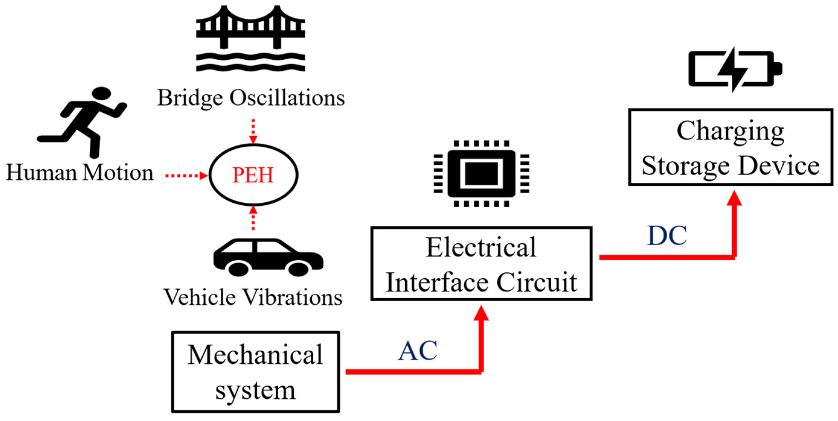
:1. Introduction
- The proposed circuit implemented a single MOSFET switch. This reduced stress in the switching process, thus achieving a higher output voltage (Vdc) and power.
- As highlighted in the literature, it is developed without employing complex, extraneous circuits and polarity indicators, which leads to lower conversion losses and complexity.
2. Piezoelectric Energy Harvesting Circuits
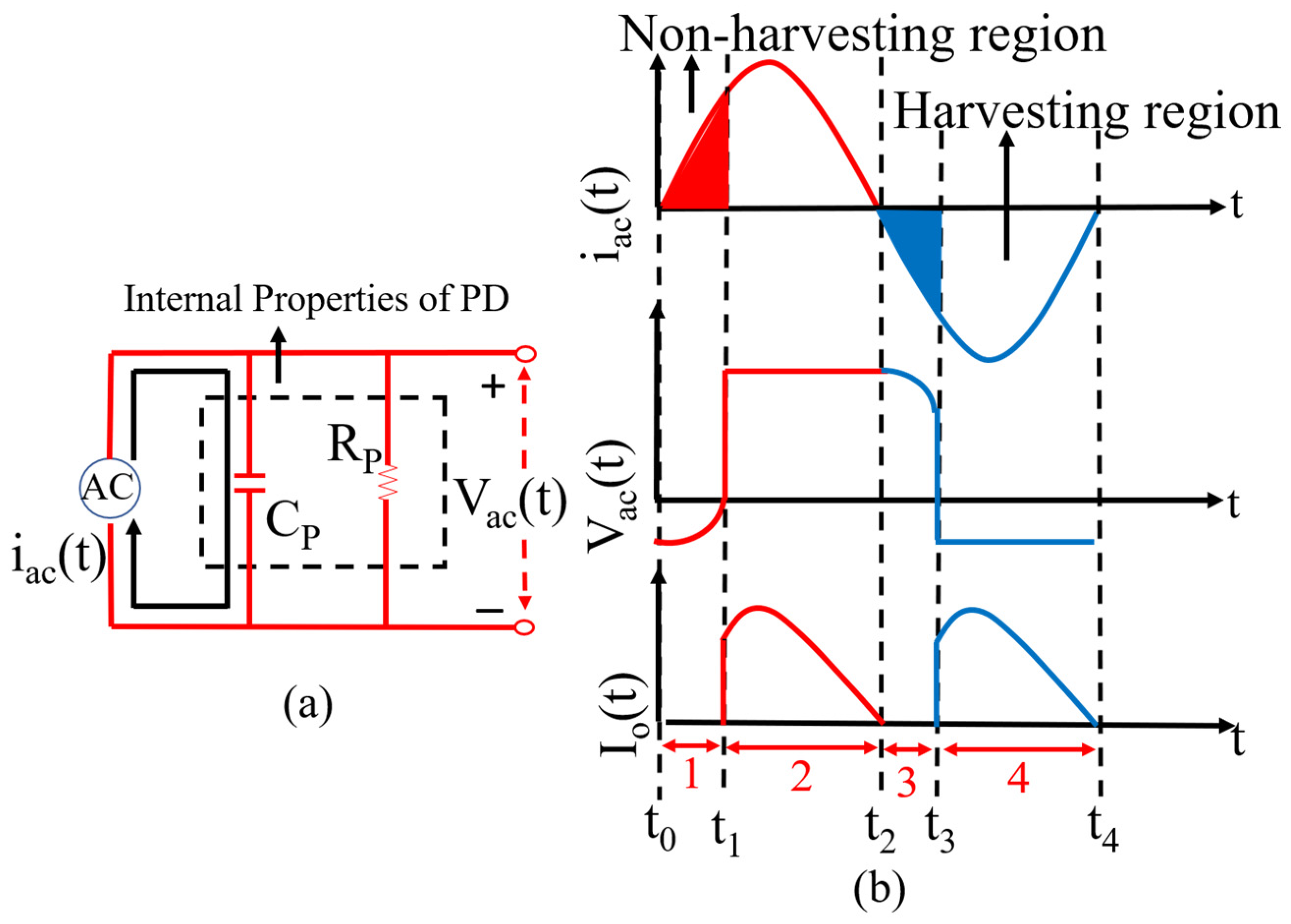
2.1. Internal Circuit of a Piezoelectric Device
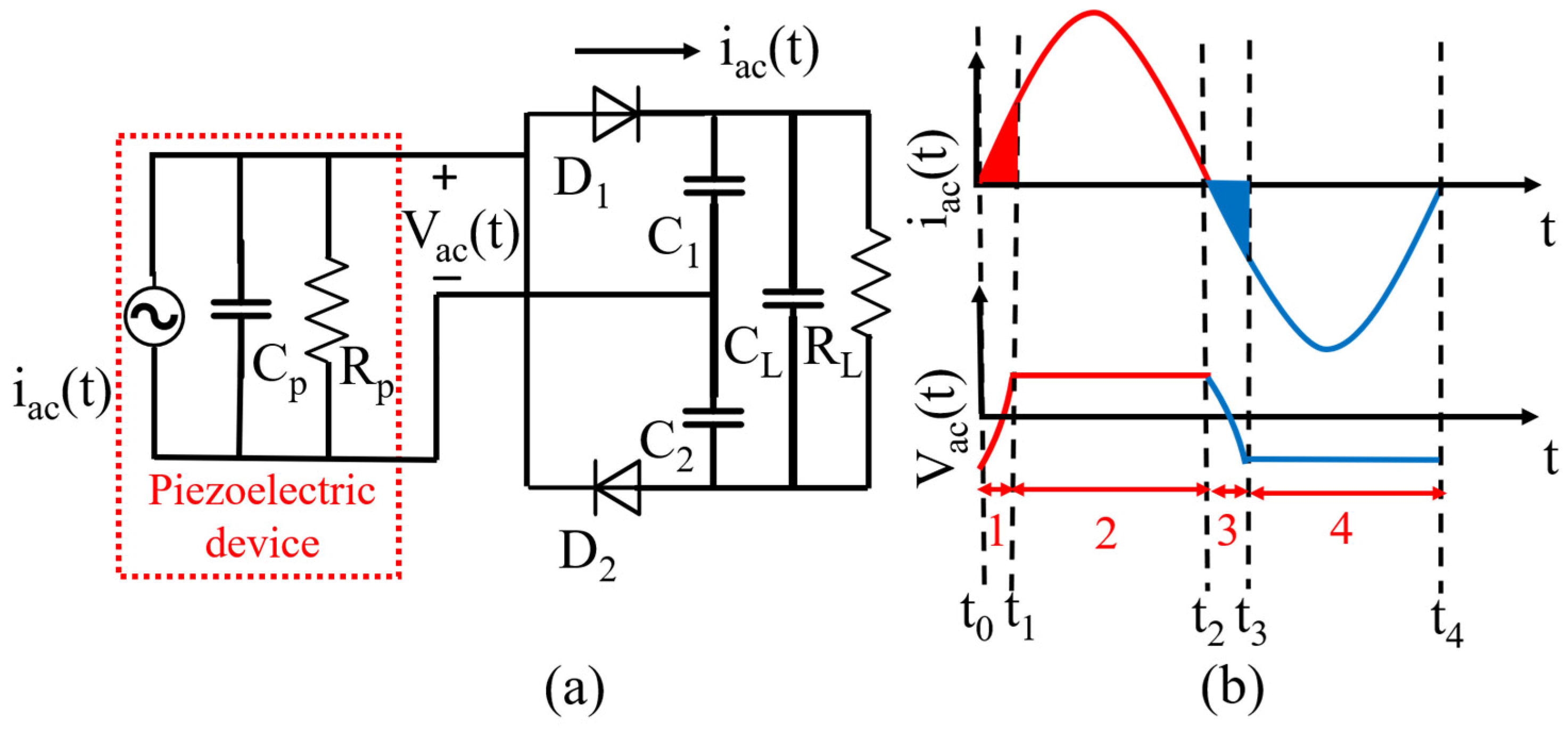
2.2. Voltage Doubler Circuit
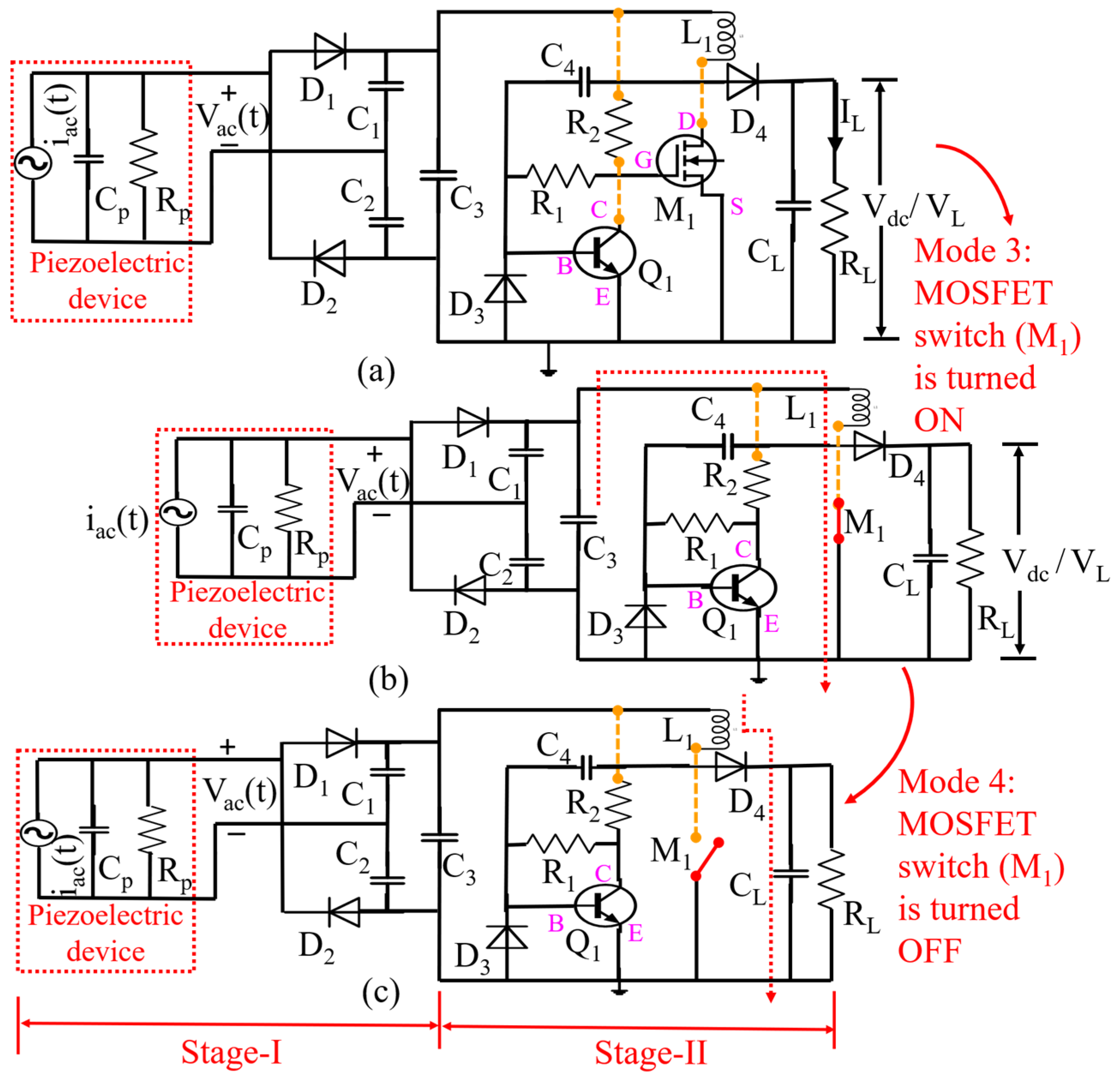
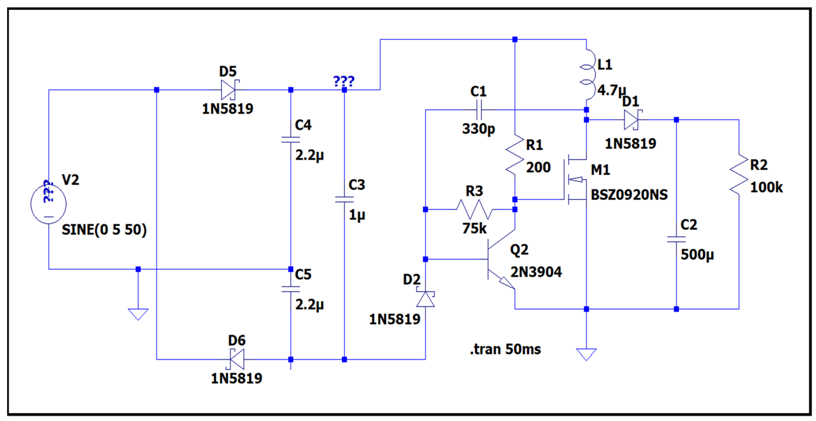
2.3. Operation Modes of the Dual-Stage Boost Convereter Circuit
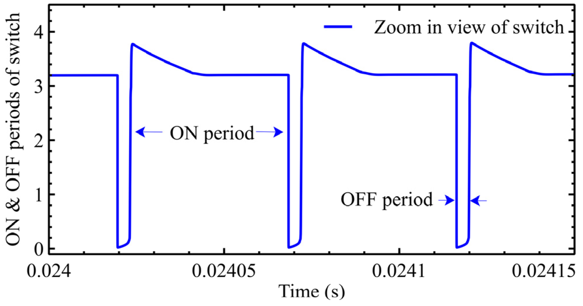
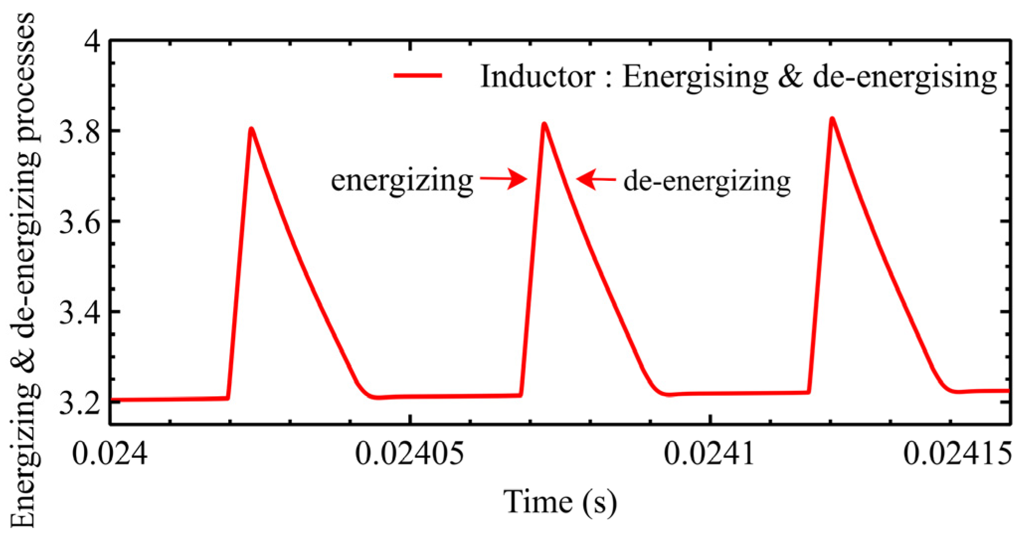
- Mode 3: (When the MOSFET switch (M1) is ON)
- Mode 4: (When the MOSFET switch (M1) is OFF)
3. Simulation Study
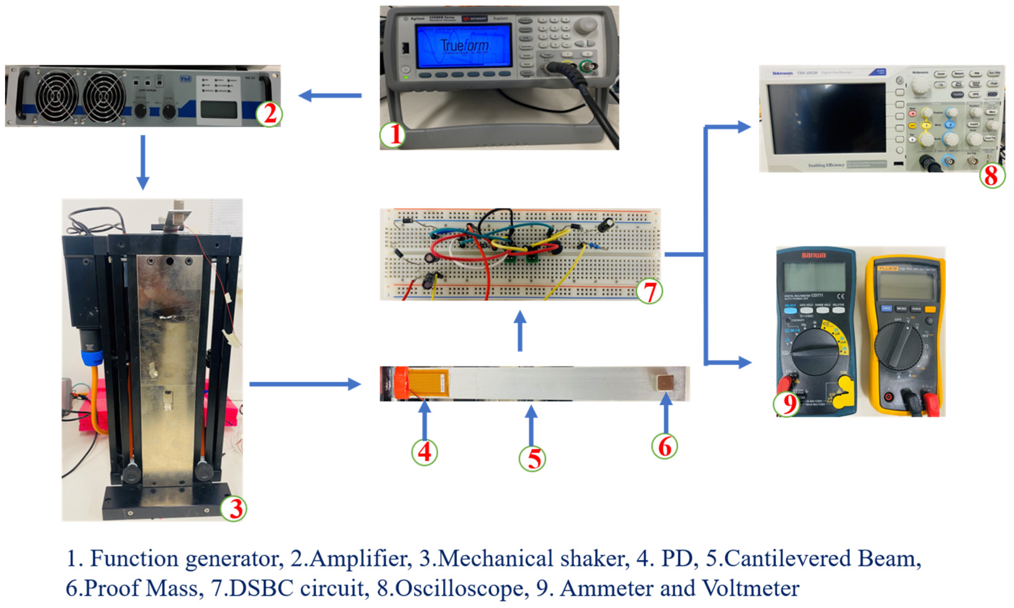
4. Experimental Study
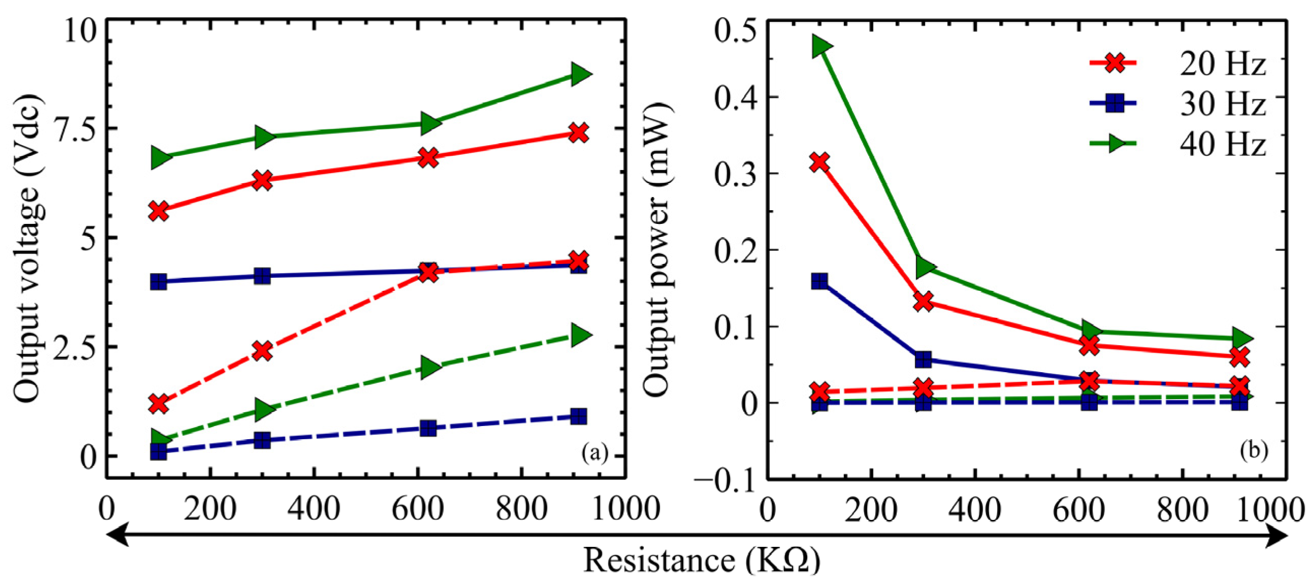
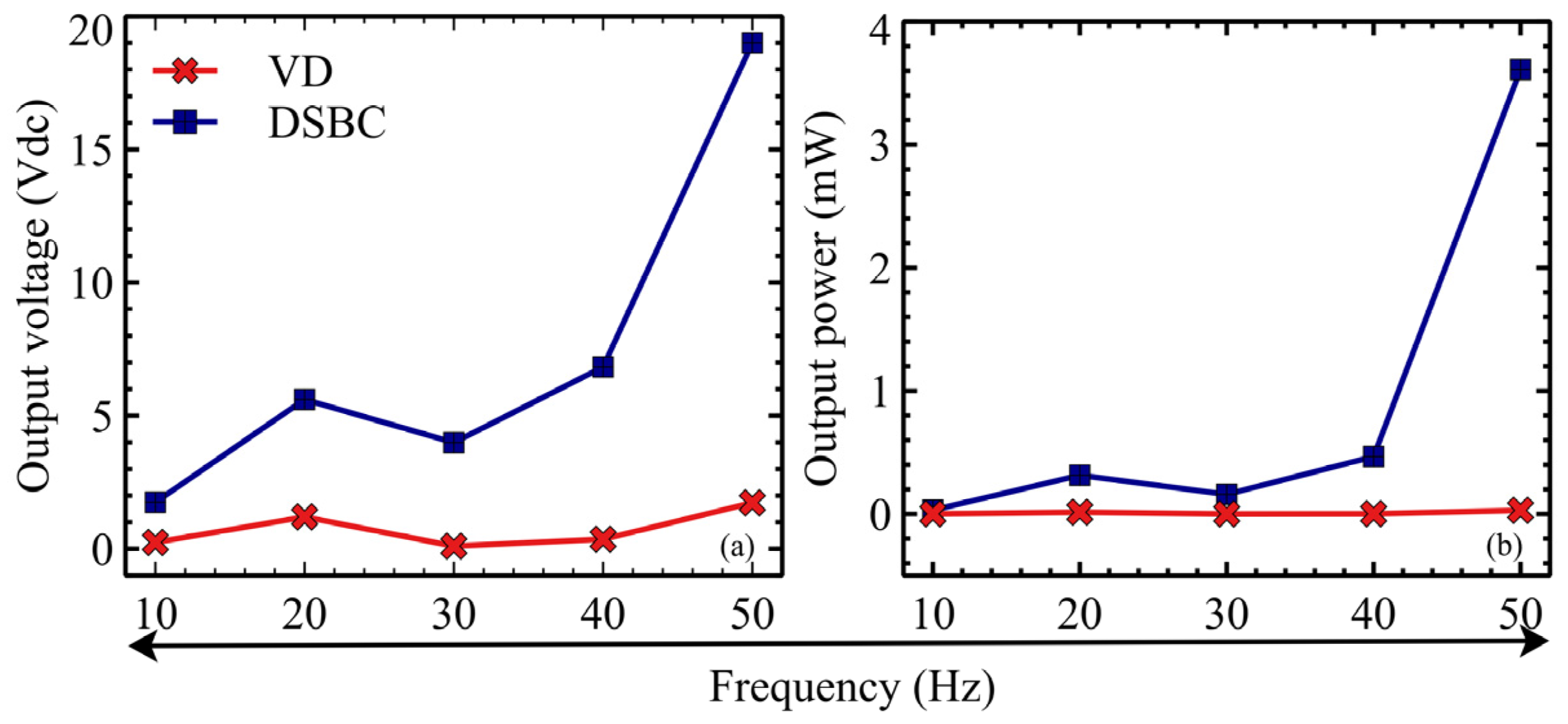
4.1. Test 1: Varying Excitation Frequency under a Constant Input Voltage
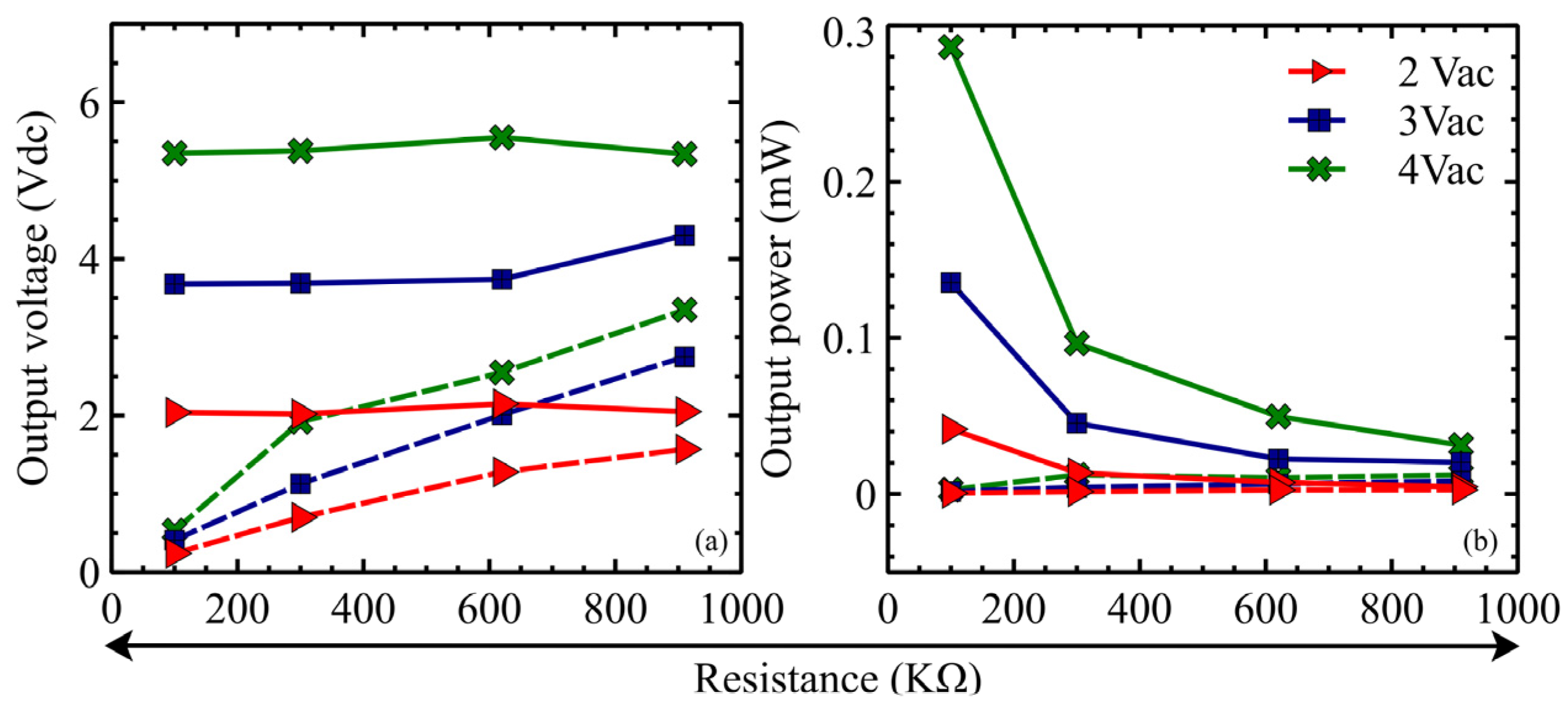
4.2. Test 2: Varying Input Voltage under a Constant Excitation Frequency
5. Conclusions
Author Contributions
Funding
Data Availability Statement
Conflicts of Interest
References
- Rand, B.P.; Genoe, J.; Heremans, P.; Poortmans, J. Solar cells utilizing small molecular weight organic semiconductors. Prog. Photovolta. Res. Appl. 2007, 15, 659–676. [Google Scholar] [CrossRef] [Green Version]
- De Broe, A.M.; Drouilhet, S.; Gevorgian, V. A peak power tracker for small wind turbines in battery charging applications. IEEE Trans. Energy Convers. 1999, 14, 1630–1635. [Google Scholar] [CrossRef]
- Sebald, G.; Pruvost, S.; Guyomar, D. Energy harvesting based on Ericsson pyroelectric cycles in a relaxor ferroelectric ceramic. Smart Mater. Struct. 2007, 17, 015012. [Google Scholar] [CrossRef]
- Edla, M.; Lim, Y.Y. An improved piezoelectric energy harvesting circuit for reducing the internal loss. In Proceedings of the 83rd Researchfora International Conference, New Delhi, India, 29 January 2020; pp. 4–8. [Google Scholar]
- Izadgoshasb, I.; Lim, Y.Y.; Tang, L.; Padilla, R.V.; Tang, Z.S.; Sedighi, M. Improving efficiency of piezoelectric based energy harvesting from human motions using double pendulum system. Energy Convers. Manag. 2019, 184, 559–570. [Google Scholar] [CrossRef]
- Wu, L.; Kang, W.; Xie, M.; Zhu, P. A self-powered multi-input bridgeless series-SSHI circuit for piezoelectric energy harvesting. In Proceedings of the 2021 IEEE International Symposium on Circuits and Systems (ISCAS), Daegu, Republic of Korea, 22–28 May 2021; pp. 1–4. [Google Scholar]
- Edla, M.; Lim, Y.Y.; Padilla, R.V.; Deguchi, M. An improved rectifier circuit for piezoelectric energy harvesting from human motion. Appl. Sci. 2021, 11, 2008. [Google Scholar] [CrossRef]
- Szarka, G.D.; Stark, B.H.; Burrow, S.G. Review of power conditioning for kinetic energy harvesting systems. IEEE Trans. Power Electron. 2011, 27, 803–815. [Google Scholar] [CrossRef]
- Chalasani, S.; Conrad, J.M. A survey of energy harvesting sources for embedded systems. In Proceedings of the IEEE Southeastcon 2008, Huntsville, AL, USA, 3–6 April 2008; pp. 442–447. [Google Scholar]
- Edla, M.; Lim, Y.Y.; Deguchi, M.; Padilla, R.V.; Izadgoshasb, I. An improved self-powered H-bridge circuit for voltage rectification of piezoelectric energy harvesting system. IEEE J. Electron Devices Soc. 2020, 8, 1050–1062. [Google Scholar] [CrossRef]
- Cheng, S.; Jin, Y.; Rao, Y.; Arnold, D.P. A bridge voltage doubler AC/DC converter for low-voltage energy harvesting applications. In Proceedings of the PowerMEMS 2009, Washington, DC, USA, 1–4 December 2009; pp. 25–28. [Google Scholar]
- Du, S.; Amaratunga, G.A.; Seshia, A.A. A cold-startup SSHI rectifier for piezoelectric energy harvesters with increased open-circuit voltage. IEEE Trans. Power Electron. 2018, 34, 263–274. [Google Scholar] [CrossRef]
- Edla, M.; Lim, Y.Y.; Mikio, D.; Padilla, R.V. A single-stage rectifier-less boost converter circuit for piezoelectric energy harvesting systems. IEEE Trans. Energy Convers. 2021, 37, 505–514. [Google Scholar] [CrossRef]
- Edla, M.; Lim, Y.Y.; Deguchi, M.; Padilla, R.V. A Novel Discontinuous Mode Piezoelectric Energy Harvesting Circuit for Low-Voltage Applications. In Proceedings of the 2021 31st Australasian Universities Power Engineering Conference (AUPEC), Perth, Australia, 26–30 September 2021; pp. 1–5. [Google Scholar]
- Edla, M.; Lim, Y.Y.; Padilla, R.V.; Mikio, D. Design and Application of a Self-Powered Dual-Stage Circuit for Piezoelectric Energy Harvesting Systems. IEEE Access 2021, 9, 86954–86965. [Google Scholar] [CrossRef]
- Srinivasan, R.; Mangalanathan, U.; Gandhi, U.; Karlmarx, L.R. Bridgeless active rectifier for piezoelectric energy harvesting. IET Circuits Devices Syst. 2019, 13, 1078–1085. [Google Scholar] [CrossRef]
- Dini, M.; Romani, A.; Filippi, M.; Tartagni, M. A nanopower synchronous charge extractor IC for low-voltage piezoelectric energy harvesting with residual charge inversion. IEEE Trans. Power Electron. 2015, 31, 1263–1274. [Google Scholar] [CrossRef]
- Du, S.; Jia, Y.; Zhao, C.; Amaratunga, G.A.; Seshia, A.A. A nail-size piezoelectric energy harvesting system integrating a MEMS transducer and a CMOS SSHI circuit. IEEE Sens. J. 2019, 20, 277–285. [Google Scholar] [CrossRef] [Green Version]
- Eltamaly, A.M.; Addoweesh, K. Self Power SSHI Circuit for Piezoelectric Energy Harvester. U.S. Patent 9,548,680, 17 January 2017. [Google Scholar]
- Lee, M.; Yang, J.; Park, M.-J.; Jung, S.-Y.; Kim, J. Design and analysis of energy-efficient single-pulse piezoelectric energy harvester and power management IC for battery-free wireless remote switch applications. IEEE Trans. Circuits Syst. I Regul. Pap. 2017, 65, 366–379. [Google Scholar] [CrossRef]
- Lefeuvre, E.; Badel, A.; Brenes, A.; Seok, S.; Woytasik, M.; Yoo, C.-S. Analysis of piezoelectric energy harvesting system with tunable SECE interface. Smart Mater. Struct. 2017, 26, 035065. [Google Scholar] [CrossRef]
- Pollet, B.; Despesse, G.; Costa, F. A new non-isolated low-power inductorless piezoelectric dc–dc converter. IEEE Trans. Power Electron. 2019, 34, 11002–11013. [Google Scholar] [CrossRef]
- Xia, H.; Xia, Y.; Shi, G.; Ye, Y.; Wang, X.; Chen, Z.; Jiang, Q. A self-powered S-SSHI and SECE hybrid rectifier for PE energy harvesters: Analysis and experiment. IEEE Trans. Power Electron. 2020, 36, 1680–1692. [Google Scholar] [CrossRef]
- Xia, H.; Xia, Y.; Ye, Y.; Qian, L.; Shi, G.; Chen, R. Analysis and simulation of synchronous electric charge partial extraction technique for efficient piezoelectric energy harvesting. IEEE Sens. J. 2018, 18, 6235–6244. [Google Scholar] [CrossRef]
- Liang, J.; Liao, W.-H. Improved design and analysis of self-powered synchronized switch interface circuit for piezoelectric energy harvesting systems. IEEE Trans. Ind. Electron. 2011, 59, 1950–1960. [Google Scholar] [CrossRef]
- Tabesh, A.; Fréchette, L.G. A low-power stand-alone adaptive circuit for harvesting energy from a piezoelectric micropower generator. IEEE Trans. Ind. Electron. 2009, 57, 840–849. [Google Scholar] [CrossRef] [Green Version]
- Shareef, A.; Goh, W.L.; Narasimalu, S.; Gao, Y. A rectifier-less AC–DC interface circuit for ambient energy harvesting from low-voltage piezoelectric transducer array. IEEE Trans. Power Electron. 2018, 34, 1446–1457. [Google Scholar] [CrossRef]
- Lefeuvre, E.; Audigier, D.; Richard, C.; Guyomar, D. Buck-boost converter for sensorless power optimization of piezoelectric energy harvester. IEEE Trans. Power Electron. 2007, 22, 2018–2025. [Google Scholar] [CrossRef]
- Kushino, Y.; Koizumi, H. Piezoelectric energy harvesting circuit using full-wave voltage doubler rectifier and switched inductor. In Proceedings of the 2014 IEEE Energy Conversion Congress and Exposition (ECCE), Pittsburgh, PA, USA, 14–18 September 2014; pp. 2310–2315. [Google Scholar]
- Rashid, M.H. Power Electronics Handbook; Butterworth-Heinemann: Oxford, UK, 2017. [Google Scholar]
- Erturk, A.; Inman, D.J. Piezoelectric Energy Harvesting; John Wiley & Sons: Hoboken, NJ, USA, 2011. [Google Scholar]
- Lu, S.; Boussaid, F. A highly efficient P-SSHI rectifier for piezoelectric energy harvesting. IEEE Trans. Power Electron. 2015, 30, 5364–5369. [Google Scholar] [CrossRef] [Green Version]
- Eltamaly, A.M.; Addoweesh, K.E. A novel self-power SSHI circuit for piezoelectric energy harvester. IEEE Trans. Power Electron. 2016, 32, 7663–7673. [Google Scholar] [CrossRef]
- Mikkelsen, J.H. Ltspice—An Introduction; Technical Report; Institute of Electronic Systems, Aalborg University: Aalborg, Denmark, 2005. [Google Scholar]
- Kwon, D.; Rincón-Mora, G.A. A 2-µm BiCMOS rectifier-free AC–DC piezoelectric energy harvester-charger IC. IEEE Trans. Biomed. Circuits Syst. 2010, 4, 400–409. [Google Scholar] [CrossRef]
- Romani, A.; Filippi, M.; Tartagni, M. Micropower design of a fully autonomous energy harvesting circuit for arrays of piezoelectric transducers. IEEE Trans. Power Electron. 2013, 29, 729–739. [Google Scholar] [CrossRef]


| Electronic Circuits | Mode 1: Positive Half-Cycle | Mode 2: Negative Half-Cycle | ||
|---|---|---|---|---|
| Interval 1 | Interval 2 | Interval 3 | Interval 4 | |
| Piezoelectric device | When to < t ≤ t1
| When t1 < t ≤ t2
| When t2 < t ≤ t3
| When t3 < t ≤ t4
|
| Voltage doubler | When to < t ≤ t1
| When t1 < t ≤ t2
| When t2 < t ≤ t3
| When t3 < t ≤ t4
|
| Dual-Stage Boost Converter Circuit | Mode 3 | Mode 4 |
|---|---|---|
| Stage II | M1: ON L1: Charging D4: OFF CL: Discharging | M1: OFF L1: Discharging D4: ON CL: Charging |
| Part | Description | |
|---|---|---|
| Type | Reference | |
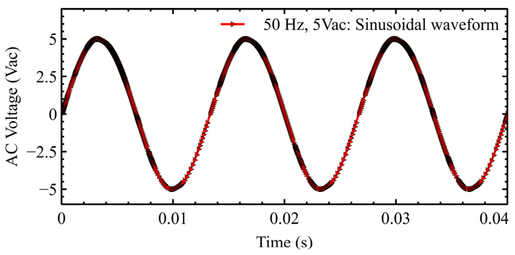
| Vac | Voltage source | 5 V, 50 Hz |
| R1 | Resistor | 75 KΩ |
| R2 | Resistor | 200 Ω |
| RL | Load Resistor | 100 Ω |
| C1–C2 | Capacitor | 2.2 uF |
| C3 | Capacitor | 330 pF |
| CL | Load Capacitor | 500 uF |
| D1–D4 | Schottky diode | 1N5819 |
| M1 | N-MOSFET | BSZ0920NS |
| Q1 | NPN-Transistor | 2N3904 |
| L1 | Inductor | 4.7 uH |
| Sources of Excitation | Test Scenarios | Frequency (Hz) | Input Voltage (Vac) | Type of Piezoelectric Device | Load Resistors (KΩ) |
|---|---|---|---|---|---|
| Mechanical Shaker | Test 1 | 1, 2, 3, 4, 5 10, 20, 30, 40, 50 | 5 3 | MFC | R1 = 100 R2 = 300 R3 = 620 R4 = 910 |
| Test 2 | 1, 2 | 1, 2, 3, 4, 5 |
| Circuit Sources | No. of Piezoelectric Devices | Input Voltage (Vac) | DC Voltage (Vdc) | Output Power (µ/mW) | External Power Supply |
|---|---|---|---|---|---|
| [35] | 1 | 1.2 | - | 30 µW | YES |
| [36] | 3 | 20 | - | 33 µW | YES |
| [15] | 1 | 5 | - | 22 µW | NO |
| [27] | 3 | 3.5 | - | 254 µW | YES |
| Proposed circuit | 1 | 3 | 19 | 3.61 mW | NO |
Disclaimer/Publisher’s Note: The statements, opinions and data contained in all publications are solely those of the individual author(s) and contributor(s) and not of MDPI and/or the editor(s). MDPI and/or the editor(s) disclaim responsibility for any injury to people or property resulting from any ideas, methods, instructions or products referred to in the content. |
© 2023 by the authors. Licensee MDPI, Basel, Switzerland. This article is an open access article distributed under the terms and conditions of the Creative Commons Attribution (CC BY) license (https://creativecommons.org/licenses/by/4.0/).
Share and Cite
Haseeb, A.; Edla, M.; Thabet, A.M.; Deguchi, M.; Kamran, M. A Self-Powered Dual-Stage Boost Converter Circuit for Piezoelectric Energy Harvesting Systems. Energies 2023, 16, 2490. https://doi.org/10.3390/en16052490
Haseeb A, Edla M, Thabet AM, Deguchi M, Kamran M. A Self-Powered Dual-Stage Boost Converter Circuit for Piezoelectric Energy Harvesting Systems. Energies. 2023; 16(5):2490. https://doi.org/10.3390/en16052490
Chicago/Turabian StyleHaseeb, Abdul, Mahesh Edla, Ahmed Mostafa Thabet, Mikio Deguchi, and Muhammad Kamran. 2023. "A Self-Powered Dual-Stage Boost Converter Circuit for Piezoelectric Energy Harvesting Systems" Energies 16, no. 5: 2490. https://doi.org/10.3390/en16052490