Article

Ionic Storage Materials for Anodic Discoloration in Electrochromic Devices

Department of Physics, National Atomic Research Institute, Taoyuan City 325207, Taiwan
*
Author to whom correspondence should be addressed.
Energies 2023, 16(24), 8119; https://doi.org/10.3390/en16248119
Submission received: 13 October 2023 / Revised: 23 November 2023 / Accepted: 13 December 2023 / Published: 17 December 2023

Abstract

:
The ion storage layer in electrochromic devices (ECDs) stores protons or lithium ions to provide electrochemical stability and extend cycle durability. This paper reports on the performance and stability of ECDs paired with various ion storage layers (NiO, V2O5, and IrO2 films). The complementary ECD using a V2O5 ion storage layer presented the fastest response time, but the lowest optical contrast. In addition, the ECD using an IrO2 ion storage layer proved the most effective as an ion storage layer, due to its high optical modulation ability capability and long-term stability. Chronoamperometry analysis revealed that IrO2-based ECD (glass/IZTO/WO3/liquid electrolyte/IrO2/IZTO/glass) can be highly effective in modulating optical transmittance, as indicated by T = 61.5% (from Tbleaching (69.6%) to Tcoloring (8.1%)) and switching times of 5.3 s for coloring and 7.3 s for bleaching at 633 nm.

1. Introduction

Electrochromic devices (ECDs) are attracting considerable attention for use in smart windows [1], optical displays [2], and rear-view mirrors [3] due to their low power usage, reversible changing, low-power driving, large optical modulation, and good memory [1,2,3,4]. Smart windows based on electrochromic (EC) materials make it easy to control the ingress of sunlight and solar heat, reducing the energy required for heating and cooling [5]. The practical applicability of ECDs can be estimated according to electrochromic efficiency, optical contrast, response time, stability, and durability [6,7]. Satisfying all of these criteria at the same time will require the development of novel materials and novel ECD structures [5,6,7].
Researchers have developed a wide variety of electrochromic (EC) materials [8,9,10,11,12], including transition-metal oxides, such as nickel oxide (NiO) [13], tungsten oxide (WO3), molybdenum trioxide (MoO3) [14,15], niobium oxide (Nb2O5), titanium dioxide (TiO2) [16], iridium oxide (IrO2) [12], and vanadium oxide (V2O5) [17]. Oxide films can be colored anodically (Ir, Ni) or cathodically (W, Mo). Complementary electrochromic devices are another class of devices in which one anodic coloration material is combined with one cathodic coloration material within a multi-layer structure. WO3 films have been widely studied for use as cathodic materials, due to their good electrochromic properties and high stability [18]. WO3 can be reversibly switched between colorless and blue under applied positive or negative voltage, respectively [19,20]. The ion storage layer in electrochromic devices (ECDs) stores protons or lithium ions to provide electrochemical stability and extend cycle durability [21]. NiO, IrO2, and V2O5 films are commonly used as ionic storage materials in ECDs.
High optical contrast and long-term durability are the two criteria of greatest importance to the practical implementation of electrochromic devices. Note, however, that ECDs are highly susceptible to degraded optical modulation when a portion of the injected ions become trapped, i.e., cannot be extracted from the ECD. The trapping of lithium ions can have a profound effect on the performance of electrochromic thin films based on WO3 and NiO layers [22,23,24,25] undergoing lithiation and delithiation. Diao et al. [22] attributed the degradation of cycled all-solid-state WO3/NiO electrochromic devices to the trapping of lithium ions. Note that the accumulation of trapped ions can lead to mechanical degradation of the ECD material; a few researchers have addressed this issue [26,27]. The mechanism by which ion trapping undermines optical modulation and subsequent electrochromic reactions has yet to be elucidated. Furthermore, researchers have yet to explain why this degradation usually occurs in conjunction with a decrease in the charge density of inserted ions [13,28].
In this study, cycle voltammetry (CV) and chronoamperometry (CA) analyses were used to study the performance and stability of ECDs based on a variety of ion storage layers (NiO, V2O5, IrO2) [17,29,30,31]. Ion quantity and the cycle-dependent evolution of open-circuit-potential (OCP) were derived from CV curves. CA and in situ optical transmittance measurements were used to assess changes in the performance and stability of ECDs. The findings obtained in this study provide a valuable contribution to the current understanding of ion storage layers and their influence on the performance and stability of electrochromic devices.

2. Materials and Methods

2.1. Preparation of Films

After evacuating a deposition chamber to a high-vacuum base pressure of less than 1 × 10⁻⁵ torr using a turbo pump, IZTO films [32] were deposited on glass substrates (10 × 10 cm2) via DC magnetron sputtering (100 W) using an IZTO target (70 at.% In2O3 + 10 at.% SnO2 + 20 at.% ZnO) under a working pressure of 2.5 × 10⁻³ torr with argon (Ar) gas without substrate heating.
Under a base chamber pressure of less than 2 × 10⁻⁵ torr, films of WO3, NiO, V2O5, and IrO2 were respectively deposited via Cathodic arc Plasma, CAP using targets of metallic tungsten (W) (99.95% purity), metallic nickel (Ni) (99.95% purity), V2O5 (99.95% purity), or metallic iridium (Ir) (99.95% purity) under Ar/O2 gas flow at a ratio of 1/3 on finished TCO/glass substrates.
Deposition parameters are detailed in Table 1.

2.2. Fabrication of Electrochromic Devices (ECDs)

The multiple layers in a typical ECDs structure are stacked as follows: transparent electrode (300 nm)/electrochromic active electrode (200 nm)/electrolyte/counter electrode (80 nm)/transparent electrode (300 nm). The ECDs in the current study comprised an IZTO transparent electrode, a WO3 active electrochromic electrode, an electrolyte of 1M LiClO4 Propylene Carbonate (PC, C4H6O3, Sigma-Aldrich, St. Louis, MO, USA), and NiO, V2O5, or IrO2 as counter electrodes.

2.3. Experiment Details

Cycle voltammetry (CV) and chronoamperometry (CA) values (Autolab PGSTAT30, Utrecht, The Netherlands) were used to derive electrochemical characteristics. The optical transmittance of the films over a wavelength range of 300 to 900 nm was measured using an ultraviolet-visible (UV-Vis) spectrophotometer (model DH-2000-BAL, Ocean Optics, Dunedin, FL, USA) with samples in colored or bleached states.

3. Results

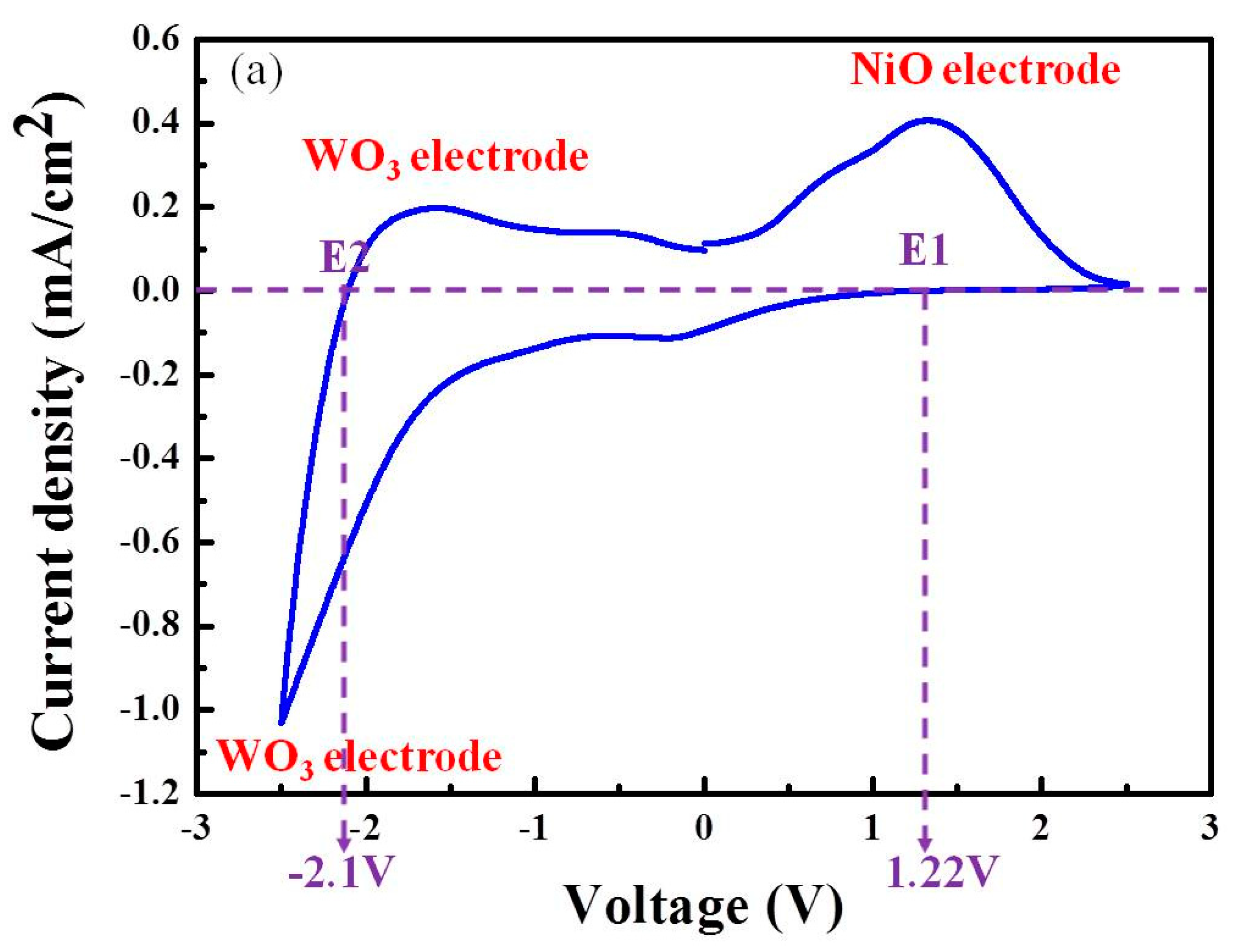
3.1. Mechanisms Underlying the Operations of Electrochromic Devices (ECD) Based on Counter Layers of NiO, V2O5, or IrO2

This study compared the electrochemical and electrochromic properties of ECDs fabricated with a matched electrochromic active layer (WO3 films) and counter layers of various materials (NiO, V2O5, or IrO2). Cycle voltammetry (CV) has been widely used to assess the electrochemical and electrochromic proprties of ECDs. CV analysis simplifies the characterization of electrochemical reactions, the charge density of inserted/extracted ions, and the elecrtrochromic efficiency of ECDs. As shown in Figure 1, under an applied negative voltage, the CV characteristics of ECDs based on IrO2 and NiO are similar to those of WO3 film, as indicated by a maximum reduction in current density at −2.5 V. Under an applied positive voltage, the NiO-based ECD underwent an initial oxidation reaction involving the WO3 electrode at −2.5 and 0 V, followed by an oxidation reaction involving NiO at 1 V. The V2O5-based ECD presented two peaks at −0.91 and −1.45 V, indicative of a reduction reaction involving a portion of the vanadium (+5) to vanadium sites (+4), which is similar to the CV characteristic curves of V2O5 films during coloration. The V2O5-based ECD also presented two peaks at −0.81 and +0.03 V, indicative of an oxidation reaction.

3.2. Electrochemical and Optical Properties as Functions of Counter Layer Types (NiO, V2O5, IrO2)

Figure 2 illustrates the in situ optical transmittance (wavelength = 633 nm) through ECDs under the effects of coloring or bleaching (voltage sweep of −2.5 V to 2.5 V) based on measurements obtained at a consistent scanning rate of 0.05 V/s. The IrO2-based ECD presented the highest optical transmittance of ∆T = 53% (from Tbleaching (67%) to Tcoloring (14%)). The optical transmittance values of the NiO-based and V2O5-based ECDs were 45% and 40%, respectively. Coloration behavior in ECDs is affected by the insertion of ions into the host structure, and ion transport behavior can be calculated according to the results of the CV envelope area under the effects of ions insertion/extraction. The charge density of inserted and extracted ions can be calculated by respectively integrating negative CV curves or positive CV curves using the following equation:
Q = I d V v
The calculated charge densities of inserted and extracted ions are shown in Figure 3. These CV test results indicate that the coloration of IrO2-based ECD and NiO-based ECDs was deeper than that of the V2O5-based ECD, due to the insertion of more ions into the electrode films. Figure 3 revealed an obvious discrepancy between inserted charge density and extracted charge density, indicating that a significant proportion of the inserted ions could not be extracted. Ions that cannot be extracted are referred to as trapped ions. The optical modulation of the NiO-based ECD failed to match that of the IrO2-based ECD, due to the trapping of an excessive number of ions in the host structure.
Ion transport behavior depends on the direction, intensity, and duration of the driving force, which is in turn dependent on the relative intensity of operation-potential (E) to open-circuit-potential (OCP). Note that OCP is defined as the voltage corresponding to net zero current flow. During a negative scan (when the response current density is zero), the voltage corresponding to this zero-current (indicated as E1) is equal to OCP1 of the ECD in a bleached state. The fact that the current generated using applied voltage E is more strongly negative than E1 induces ion insertion into the ECDs and subsequent coloring. During a positive scan (when the response current density is zero), the voltage corresponding to this zero-current (marked as E2) is equal to OCP2 of the ECD in the colored state, at which point the density of inserted ions is maximized. The fact that the current generated with applied voltage E is more strongly negative than E2 induces the extraction of ions out of the ECD and subsequent bleaching. The driving force underlying ion transport depends on the relative intensity of applied voltage E to OCP, wherein a larger gap between applied voltage E and OCP produces a stronger force to drive ion transport. The OCP values of all ECDs are listed in Table 2.
As shown in Figure 4, the ratio of inserted ions to extracted ions largely determined the driving force underlying ion transport [33]. As shown in Figure 4a, the coloration of the NiO-based ECD was examined under negative current density by sweeping the potential from 1.22 V to −2.5 V and back to −2.1 V. Figure 4b, the bleaching process of the NiO-based ECD was examined under positive current density by sweeping the potential from −2.1 V to 2.50 V and back to 1.22 V. Again, the curve representing the inserted charge ratio presented two distinct parts. The first part (voltage of 1.22 to −1.5 V) revealed gradual ion insertion, while the driving force in the second part was sufficient to induce the insertion of most ions into the WO3. Based on the same methods, the OCP values of IrO2-based ECD were as follows: OCP1 (1.03 V) and OCP2 (−2.12 V). As shown in Figure 4a, the CV curve of the IrO2-based ECD was similar to that of the NiO-based ECD; however, the curve for the inserted charge ratio could not be divided into two parts (see Figure 4). This indicates that unlike the NiO-based ECD, when E was more strongly negative than OCP1, the IrO2-based ECD did not require a strong driving force for ion insertion. When E was more strongly positive than OCP2, the curve of the extracted charge ratio appeared as a straight line, indicating that the IrO2-based ECD did not require a strong driving force for ion extraction.
As shown in Figure 4b, the coloration process of the V2O5-based ECD was examined under negative current density by sweeping the potential from 1.35 V to −2.50 V and back to −1.54 V. The bleaching process of the V2O5-based ECD was examined under positive current density by sweeping the potential from −1.54 V to 2.50 V and back to 1.35 V. The slope of the curve for the inserted/extracted charge ratio was larger in this ECD than in the other ECDs, indicating that the insertion/extraction of ions could be achieved using a weaker driving force than is required for NiO-based ECDs and IrO2-based ECDs.

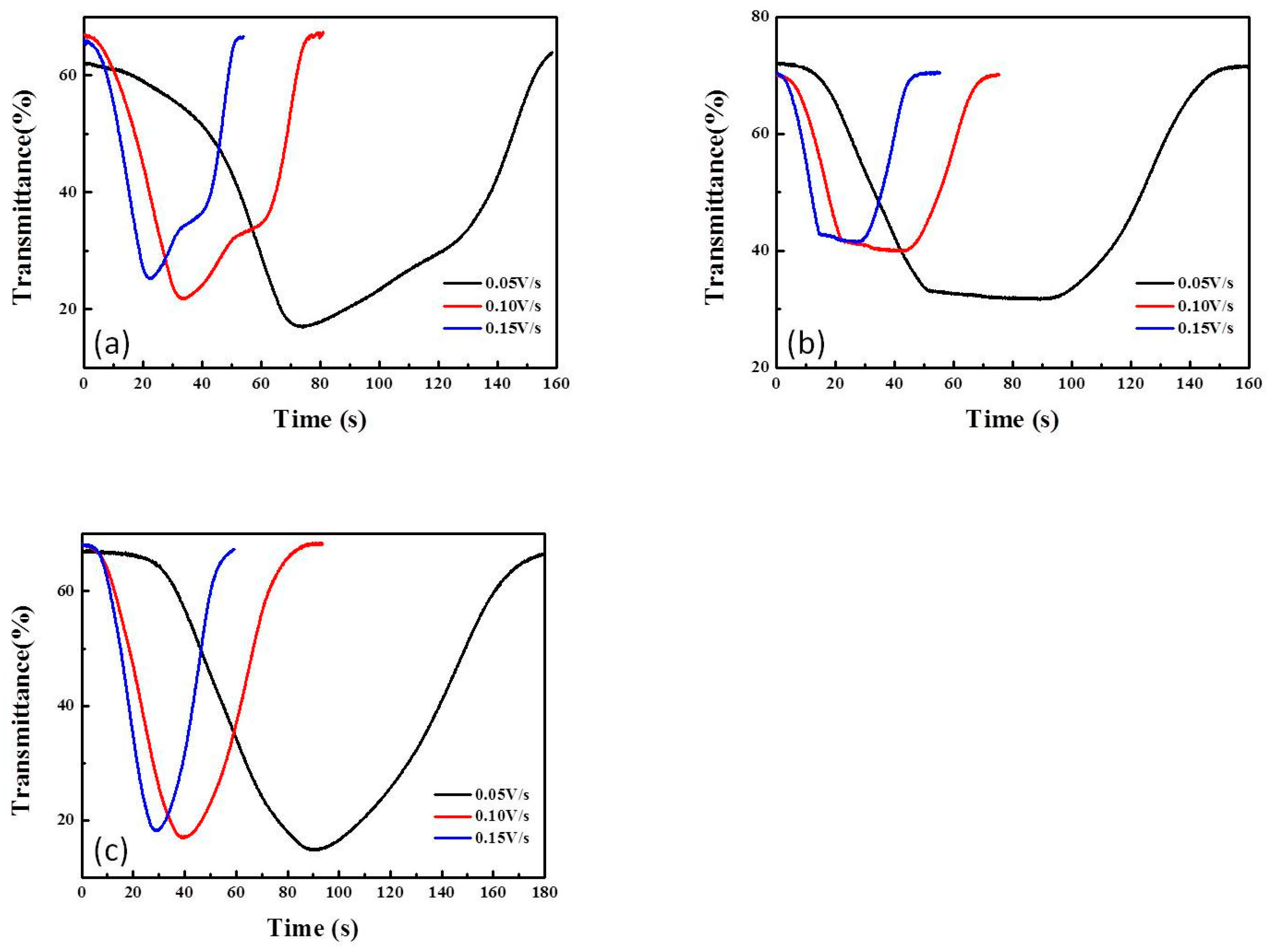
3.3. CV Curves of ECDs as a Function of Scanning Rate

Figure 5 plots current density versus voltage potential in the first cycle of applied sweep voltage ranging from −2.5 V to 2.5 V at scanning rates of 0.05, 0.10, and 0.15 V/s. The area under the CV curve of all three ECDs increased with the scanning rate. Figure 6 presents the charge density of inserted and extracted ions, as calculated using Equation (1). Our results revealed that charge density varied directly with the area under the CV curve, but inversely with scanning rate. The minimum charge density of all three ECD types was 0.15 mA/cm2 (regardless of scanning rate), with scanning rates higher than 0.1 V/s and 0.05 V/s. Figure 6d illustrates the relationship between the charge density of trapped ions versus the scanning rate. Overall, slower scanning rates were associated with the trapping of more ions.
Figure 7 presents the in situ optical transmittance (wavelength = 633 nm) of the three ECDs throughout the coloring/bleaching processes. All three ECDs presented the deepest coloration (i.e., the most pronounced optical modulation) under the slowest scanning rate (0.05 V/s). During the CV test, the ion storage capacity and optical modulation of the ECDs varied with the scanning rate.

3.4. ECD Performance: Long-Term Stability and Durability

The long-term stability of ECDs is crucial to their practical applicability in the real world. The ECD must be resistant to the accumulation of trapped ions (Qtrap), which can be calculated as follows:
Q t r a p = 1 m 1 R × Q i n d n
where Qin refers to the number of inserted ions, while R refers to ion transport reversibility expressed as the ratio of extracted ions to inserted ions. Qtrap depends on Qin and the degree of reversibility. Figure 8 compares the three ECDs in terms of long-term durability (100 CV cycles). Overall, the shapes of the CV curves and peak positions did not vary throughout the 100 cycles.
Figure 9 illustrates the evolution of the charges associated with the inserted/extracted ions (as derived using Equation (2)). Under 0.05 V, all three ECDs exhibited capacity degradation throughout the 100 cycles. As shown in Figure 9d, the reversibility (R) of the V2O5-based ECD (0.97~1.02) exceeded that of the other ECDs, and the quantity of inserted ions was lower. The NiO-based ECD presented the lowest overall R and the smallest quantity of inserted ions. Accordingly, the three materials were ranked according to the quantity of trapped ions as follows: NiO > IrO2 > V2O5. Taken together, it appears that R was inversely proportional to the quantity of trapped ions and the likelihood of ion blocking, which can affect the driving force and time-evolution required for ion insertion.
Figure 10 presents the OCP values in the 1st cycle versus the 100th cycle. We determined that in the bleaching state, the OCP of the NiO and IrO2-based ECDs shifted to a more negative potential, whereas the OCP of the V2O5-based ECD shifted to a more positive potential, due to the accumulation of trapped ions. The electric field force required to drive ions into the ECD depends on the relative intensity of operation potential to OCP in the negative direction. Figure 11 plots the inserted charge ratio versus driving force as a function of cycle number under an applied sweep voltage of −2.5 V to 2.5 V at a scanning rate of 0.05. The NiO-based ECD presented an obvious decay in the inserted charge ratio as a function of driving force, due to the accumulation of trapped ions.
Coloration in the NiO-based ECD in the 1st cycle occurred under an applied voltage of 1.22 V to −2.50 V, and the ion insertion time (based on the ratio of potential to a scanning rate of 0.05 V/s) was 82.4 s. Coloration after 100 cycles occurred under 1.07 V to −2.50 V, and the ion insertion time was 79 s. Coloration in the IrO2-based ECD required negative voltage and the ion insertion time decreased with the number of cycles. It is interesting to note that the evolution of OCP in the V2O5-based ECD was reversed. Essentially, the R value was higher in the 100th cycle than in the 1st cycle, indicating a reduction in the quantity of accumulated ions.
Figure 12 presents the CA curves of all ECDs as a function of voltage potential (−2.0 V to 2.0 V) over a period of 30 s, and the corresponding in situ transmittance response under a fixed wavelength of 633 nm. The modulation of optical transmittance by the IrO2-based ECD (∆T = 61.5%; from Tbleaching (69.6%) to Tcoloring (8.1%)) exceeded that of the other ECDs. Note that the modulation of optical transmittance based on CA curves was qualitatively the same as that based on CV curves. The speed of coloration and bleaching (i.e., switching times) are crucial to the effectiveness of ECD systems. Switching time is defined as the time required to achieve a change in transmittance equivalent to 90% of full modulation. Figure 12 was evaluated tc values were as follows: NiO-based ECD (13.9 s), V2O5-based ECD (2.1 s), and IrO2-based ECDs (5.3 s). The tb values were as follows: NiO-based ECD (5.7 s), V2O5-based ECD (2.1 s), and IrO2-based ECDs (7.3 s). Overall, the switching of the V2O5-based ECD was faster than that of the other ECDs, due presumably to the underlying electrochromic mechanism.

4. Conclusions

The practical applicability of ECDs can be assessed in terms of electrochromic efficiency, optical contrast, response time, stability, and durability. This paper reports on the use of cycle voltammetry (CV) and chronoamperometry (CA) to investigate the performance and stability of composite ECDs based on various ion storage layers (NiO, V2O5, or IrO2 films). In CV analysis, the ECD with a V2O5 ion storage layer demonstrated response times faster than those of the other devices and required less driving force, due to the fact that the electrochromic mechanism in this device is primarily affected by the V2O5 layer. Note, however, that the optical contrast of the V2O5-based ECD was lower than that of the other devices. The long-term stability of ECDs is determined largely by the quantity of trapped ions. During the CV test, the accumulation of trapped ions was shown to decrease optical modulation ability and increase the driving force required for ion transport. Thus, the reversibility of the IrO2-based ECD exceeded that of the NiO-based ECD, which accumulated a large quantity of trapped ions. Overall, IrO2 provided the most effective ion storage layer in terms of optical modulation ability and long-term stability.

Author Contributions

Formal data analysis, C.-T.C. and P.-H.K.; project administration, P.-W.C.; writing—original draft, P.-W.C. All authors have read and agreed to the published version of the manuscript.

Funding

This research was funded by the Department of Physics, National Atomic Research Institute (NARI), Taiwan.

Data Availability Statement

The data presented in this study are available on request from the corresponding author. The data are not publicly available due to privacy.

Conflicts of Interest

The authors declare no conflict of interest.

References

  1. Granqvist, C.G. Electrochromics for smart windows: Oxide-based thin films and devices. Thin Solid Films 2014, 564, 1–38. [Google Scholar] [CrossRef]
  2. Chang, J.Y.; Chen, Y.C.; Wang, C.M.; Wang, W.N.; Wen, C.Y.; Lin, J.M. Electrochromic properties of Lithium-doped tungsten oxide prepared by electron beam evaporation. Coatings 2019, 9, 191. [Google Scholar] [CrossRef]
  3. Kim, K.H.; Koo, B.R.; Ahn, H.J. Sheet resistance dependence of fluorine-doped tin oxide films for high-performance electrochromic devices. Ceram. Int. 2018, 44, 9408–9413. [Google Scholar] [CrossRef]
  4. Jiang, B.; Lou, B.; Li, J.; Peng, P.; Chen, J.W.; Chu, L.H.; Li, Y.F.; Li, M.C. Electrochemical effect of graphite fluoride modification on Li-rich cathode material in lithium ion battery. Ceram. Int. 2019, 45, 160–167. [Google Scholar] [CrossRef]
  5. Yiying, H.; Zhuo, G.; Yufei, P.; Peng, G.; Yu, P.; Jiayu, T.; Xiao-Peng, Z.; Jian, L. Molecular engineering of π-extended viologens with four arms for efficient and tunable electrochromic devices. Dye. Pigment. 2023, 219, 111556. [Google Scholar]
  6. Yu, P.; Peng, G.; Hongjin, C.; Xiao-Peng, Z.; Yiying, H.; Zhuo, G.; Jinkun, X.; Rui, Z.; Jian, L. Electropolymerization of D-A type monomers consisting of mono-triphenylamine moiety for electrochromic devices and supercapacitors. J. Mol. Struct. 2023, 1292, 136182. [Google Scholar]
  7. Jiayu, T.; Hongjin, C.; Yiying, H.; Lang, P.; Xiao-Peng, Z.; Sheng, P.; Zhirong, W.; Haitao, L.; Jian, L. Electropolymerization of D-A-D type triphenlyamine-based monomers consisting of camphor substituted quinoxaline unit for efficient electrochromism and supercapacitors. Polymer 2023, 285, 126386. [Google Scholar]
  8. Phan, G.T.; Pham, D.V.; Patil, R.A.; Tsai, C.H.; Lai, C.C.; Yeh, W.C.; Liou, Y.; Ma, Y.R. Fast-switching electrochromic smart windows based on NiO-nanorods counter electrode. Sol. Energy Mater. Sol. Cells 2021, 231, 111306. [Google Scholar] [CrossRef]
  9. Zhang, W.; Li, H.; Yu, W.W.; Elezzabi, A.Y. Excitonic complexes and optical gain in two-dimensional molybdenum ditelluride well below the Mott transition. Light Sci. Appl. 2020, 9, 121. [Google Scholar] [CrossRef] [PubMed]
  10. Lee, C.; Oh, Y.; Yoon, I.S.; Kim, S.H.; Ju, B.K.; Hong, J.M. Flash-induced nanowelding of silver nanowire networks for transparent stretchable electrochromic devices. Sci. Rep. 2018, 8, 2763. [Google Scholar] [CrossRef] [PubMed]
  11. Granqvist, C.G.; Arvizu, M.A.; Pehlivan, I.B.; Qu, H.Y.; Wen, R.T.; Niklasson, G.A. Electrochromic materials and devices for energy efficiency and human comfort in buildings: A critical review. Electrochim. Acta 2018, 259, 1170. [Google Scholar] [CrossRef]
  12. Wei, Y.X.; Ma, Y.B.; Chen, M.; Liu, W.M.; Li, L.; Yan, Y. Electrochemical investigation of electrochromic device based on WO3 and Ti doped V2O5 films by using electrolyte containing ferrocene. J. Electroanal. Chem. 2017, 807, 45–51. [Google Scholar] [CrossRef]
  13. Niklasson, G.A.; Granqvist, C.G. Sol-gel fabrication of NiO and NiO/WO3 based electrochromic device on ITO and flexible substrate. Ceram. Int. 2020, 46, 8631–8639. [Google Scholar]
  14. Chang, C.C.; Chi, P.W.; Chandan, P.; Lin, C.K. Electrochemistry and Rapid ElectrochromismControl of MoO3/V2O5 Hybrid Nano bilayers. Nat. Mater. 2019, 12, 2475. [Google Scholar] [CrossRef]
  15. Ding, J.; Abbas, S.A.; Hanmandlu, C.; Lin, L.; Lai, C.S.; Wang, P.C.; Li, L.J.; Chu, C.W.; Chang, C.C. Facile synthesis of carbon/MoO3 nanocomposites as stable battery anodes. J. Power Sources 2017, 348, 270. [Google Scholar] [CrossRef]
  16. Akkurt, N.; Pat, S.; Mohammadigharehbagh, R.; Özgür, M.; Demirkol, U.; Olkun, A.; Korkmaz, Ş. Investigation of TiO2 thin films as a cathodic material for electrochromic display devices. J. Mater. Sci. 2020, 31, 9568–9578. [Google Scholar] [CrossRef]
  17. Li, H.; McRae, L.; Elezzabi, A.Y. Solution-processed interfacial PEDOT: PSS assembly into porous tungsten molybdenum oxide nanocomposite films for electrochromic applications. ACS Appl. Mater. Interfaces 2018, 10, 10520–10527. [Google Scholar] [CrossRef]
  18. Eren, E.; Alver, C.; Karaca, G.Y.; Uygun, E.; Oksuz, L.; Oksuz, A.Y. High-performance Flexible Complementary Electrochromic Device Based on Plasma Modified WO3 Nano Hybrids and V2O5 Nanofilm with Low Operation Voltages. Electroanalysis 2018, 30, 2099–2109. [Google Scholar] [CrossRef]
  19. Kim, C.-Y.; Cho, S.-G.; Lim, T.-Y. Cycle test and degradation analysis of WO3/PC+LiClO4/CeO2·TiO2 electrochromic device. Sol. Energy Mater. Sol. Cells 2009, 93, 2056–2061. [Google Scholar] [CrossRef]
  20. Dong, D.; Wang, W.; Rougier, A.; Barnabé, A.; Dong, G.; Zhang, F.; Diao, X. Lithium trapping as a degradation mechanism of the electrochromic properties of all-solid-state WO3//NiO devices. J. Mater. Chem. C 2018, 6, 9875. [Google Scholar] [CrossRef]
  21. Wen, R.-T.; Granqvist, C.G.; Niklasson, G.A. Eliminating degradation and uncovering ion-trapping dynamics in electrochromic WO3 thin films. Nat. Mater. 2015, 14, 996. [Google Scholar] [CrossRef]
  22. Wen, R.-T.; Arvizu, M.A.; Morales-Luna, M.; Granqvist, C.G.; Niklasson, G.A. Ion Trapping and Detrapping in Amorphous Tungsten Oxide Thin Films Observed by Real-Time Electro-Optical Monitoring. Chem. Mater. 2016, 28, 4670. [Google Scholar] [CrossRef]
  23. Baloukas, B.; Arvizu, M.A.; Wen, R.-T.; Niklasson, G.A.; Granqvist, C.G.; Vernhes, R.; Klemberg-Sapieha, J.E.; Martinu, L. Galvanostatic Rejuvenation of Electrochromic WO3 Thin Films: Ion Trapping and Detrapping Observed by Optical Measurements and by Time-of-Flight Secondary Ion Mass Spectrometry. ACS Appl. Mater. Interfaces 2017, 9, 16995. [Google Scholar] [CrossRef]
  24. Runnerstrom, E.L.; Llordés, A.; Lounisac, S.D.; Milliron, D.J. Nanostructured electrochromic smart windows:traditional materials and NIR-selective plasmonic nanocrystals. Chem. Commun. 2014, 50, 10555–10572. [Google Scholar] [CrossRef]
  25. Li, H.; McRaea, L.; Firby, C.J.; Hussein, M.A.; Elezzabi, A.Y. Nanohybridization of molybdenum oxide with tungsten molybdenum oxide nanowires for solution-processed fully reversible switching of energy storing smart windows. Nano Energy 2020, 47, 130–139. [Google Scholar] [CrossRef]
  26. Chen, P.W.; Chang, C.T.; Ko, T.F.; Hsu, S.C.; Li, K.F.; Wu, J.Y. Fast response of complementary electrochromic device based on WO3/NiO electrodes. Sci. Rep. 2020, 10, 8430. [Google Scholar] [CrossRef]
  27. Li, Y.; McMaster, W.A.; Wei, H.; Chen, D.; Caruso, R.A. Enhanced electrochromic properties of WO3 Nanotree−like structures synthesized via a two-step sol-vothermal process showing promise for electrochromic window application. ACS Appl. 2018, 1, 2552–2558. [Google Scholar]
  28. Tritschler, U.; Beck, F.; Schlaad, H.; Cölfen, H. Electrochromic properties of self-organized multifunctional V2O5 polymer hybrid films. J. Mater. Chem. C 2015, 3, 950–954. [Google Scholar] [CrossRef]
  29. Chun, Y.T.; Neeves, M.; Smithwick, Q.; Placido, F.; Chu, D. High optical and switching performance electrochromic devices based on a zinc oxide nanowire with poly (methyl methacrylate) gel electrolytes. Appl. Phys. Lett. 2014, 105, 193301. [Google Scholar] [CrossRef]
  30. Xia, X.H.; Tu, J.P.; Zhang, J.; Wang, X.L.; Zhang, W.K.; Huang, H. Electrochromic properties of porous NiO thin flms prepared by a chemical bath deposition. Sol. Energy Mater Sol. Cells 2008, 92, 628–633. [Google Scholar] [CrossRef]
  31. Subrahmanyam, A.; Kumar, C.S.; Karuppasamy, K.M. A note on fast protonic solid state electrochromic device: NiOx/Ta2O5/WO3−x. Sol. Energy Mater Sol. Cells 2007, 91, 62–66. [Google Scholar] [CrossRef]
  32. Li, K.D.; Chen, P.W.; Chang, K.S.; Hsu, S.C.; Jan, D.J. Indium-Zinc-Tin-Oxide Film Prepared by Reactive Magnetron Sputtering for Electrochromic Applications. Materials 2018, 11, 2221. [Google Scholar] [CrossRef]
  33. Zhou, K.L.; Wang, H.; Liu, J.; Yan, H. The mechanism of trapped ions eroding the electrochromic performances of WO3 thin films. Int. J. Electrochem. Sci. 2018, 13, 7335. [Google Scholar] [CrossRef]
Figure 1. CV curves of ECDs fabricated using a matched electrochromic active layer (WO3 films) with counter layers comprising films of (a) NiO, (b) V2O5, and (c) IrO2.
Energies 16 08119 g001aEnergies 16 08119 g001b
Figure 2. In situ optical transmittance of ECDs at a wavelength of 633 nm under an applied sweep voltage from −2.5 V to 2.5 V with a set scanning rate of 0.05 V/s.
Energies 16 08119 g002
Figure 3. Inserted/extracted charges associated with the three ECD types.
Energies 16 08119 g003
Figure 4. Relationship between driving force and the ratio of inserted to extracted ions.
Energies 16 08119 g004
Figure 5. CV curves showing current density fluctuations as a function of scanning rate during the first cycle of sweep voltage ranging from −2.5 V to 2.5 V in ECDs based on (a) NiO, (b)V2O5, and (c) IrO2.
Energies 16 08119 g005aEnergies 16 08119 g005b
Figure 6. Charges of inserted and extracted ions based on (a) NiO, (b)V2O5, and (c) IrO2. (d) Relationship between ion trapping and scanning rate.
Energies 16 08119 g006
Figure 7. CV curves showing in situ optical transmittance (wavelength = 633 nm) as a function of scanning rate during coloring/bleaching in ECDs based on (a) NiO, (b) V2O5, and (c) IrO2.
Energies 16 08119 g007
Figure 8. CV evolutions of ECDs based on (a) NiO, (b) V2O5, and (c) IrO2.
Energies 16 08119 g008
Figure 9. Evolution of charge of inserted and extracted ions in ECDs based on (a) NiO, (b) V2O5, and (c) IrO2. (d) Evolution of reversibility.
Energies 16 08119 g009
Figure 10. Relative intensity of operation potential E to OCP and coloration range of ECDs based on (a) NiO, (b) V2O5, and (c) IrO2 (in the 1st and 100th cycles under a scanning rate of 0.05 V/s).
Energies 16 08119 g010
Figure 11. Inserted charge ratio versus driving force as a function of cycle number under an applied sweep voltage of −2.5 V to 2.5 V at a scanning rate of 0.05 for ECDs based on (a) NiO, (b) V2O5, and (c) IrO2.
Energies 16 08119 g011
Figure 12. CA curves as a function of voltage potential (−2.0 V to 2.0 V) applied for 30 s, and corresponding in situ transmittance response at a fixed wavelength of 633 nm for ECDs based on (a) NiO, (b) V2O5, and (c) IrO2.
Energies 16 08119 g012
Table 1. The deposition parameters for both the electrochromic, ion layer, and the transparent conducting layer were determined.
TargetAr/O2 (sccm)W.P.
(mTorr)
DC
Power
(W)
Deposition
Time
(min)
Deposition Rate
(nm/min)
Deposition
Temp
(°C)
Thickness
(nm)
ITO1/0
(Ar = 30)
2.5 1001030RT300
W Metal1/3
(Ar = 100)
8 1500151350200
Ni Metal1/3
(Ar = 120)
8 6503205060
V
Metal
1/3
(Ar = 20)
2.5 120012510080
Ir Metal1/3
(Ar = 120)
8 6503205060
Table 2. OCP values of the three ECD types.
OCP1OCP2
NiO-based ECD1.22 V−2.10 V
V2O5-based ECD1.35 V−1.54 V
IrO2-based ECD1.03 V−2.12 V
Disclaimer/Publisher’s Note: The statements, opinions and data contained in all publications are solely those of the individual author(s) and contributor(s) and not of MDPI and/or the editor(s). MDPI and/or the editor(s) disclaim responsibility for any injury to people or property resulting from any ideas, methods, instructions or products referred to in the content.

