Article

PV Powered High Voltage Pulse Converter with Switching Cells for Food Processing Application

1
Department of Electrical and Electronics Engineering, SRM Institute of Science and Technology, Kattankulathur 603203, India
2
Renewable Energy Lab, College of Engineering, Prince Sultan University, Riyadh 11586, Saudi Arabia
3
Department of Electrical and Electronics Engineering, B.S. Abdur Rahman Crescent Institute of Science and Technology, Chennai 600048, India
4
Mechanical Engineering Department, Faculty of Engineering, Kafrelsheikh University, Kafrelsheikh 33516, Egypt
*
Authors to whom correspondence should be addressed.
Energies 2023, 16(2), 1010; https://doi.org/10.3390/en16021010
Submission received: 2 December 2022 / Revised: 11 January 2023 / Accepted: 12 January 2023 / Published: 16 January 2023
(This article belongs to the Section A2: Solar Energy and Photovoltaic Systems)

Abstract

:
In recent years, industries in the suburb have retrofitted their power supply units with solar power supply systems. Using solar power supply systems for various applications, such as food processing, enables energy expense saving. A promising opportunity in the food industry is solar-powered Pulsed Electric Field (PEF) used in the treatment of fruits and their by-products. For this application, a converter is proposed in this paper with a combination of a passive switched inductor cell and a switched capacitor cell. Furthermore, the derived topology possesses an extendable feature. This topology generates high voltage repetitive pulses with a single semiconductor switch and a reduced component count. Dynamic study of the converter is also performed with the derivation of the transfer function. Cost effective, reliable, and simple circuitry are the critical features of this topology. The circuit topology can generate high voltage pulses by increasing the number of switched inductors and switched capacitor cells. A correlation study on the impact of the switched inductor/capacitor cell is also performed and analyzed, which is not usually performed. A 50 W prototype is designed and tested to validate the performance of the converter

1. Introduction

Recently, modern technologies have been introduced to the food processing industries to retain the nutrients in the food when it is processed. For example, moisture extraction processes to inhibit the deterioration and dehydration of vegetables and fruits have been modernized. Thermal drying, osmotic dehydration and vacuum infusions are some of the methods of dehydration. As a substitution to traditional food processing methods, non-thermal food processing techniques have gained a wide range of popularity and serve as a potential tool in fruit preservation. As a non-thermal method in food preservation, Pulsed Electric Field technology involves short electric pulses for the inactivation of micro-organisms and the dehydration of fruits and the preservation of their vital quality and nutrition. Pulsed Electric Field (PEF) stands as a low cost and low energy technology for the cell membrane permeabilization of fruit tissues [1,2]. The PEF maintains the basic structure of food without thermal degradation and a significant temperature rise [3,4]. The benefits of PEF in large scale food industry application as a standalone process, and also as a combination with various methods for the acceleration of fermented food are discussed [1].
The PEF method of microorganism inactivation is found to increase the temperature while food processing. The selection of PEF with nano second pulses can effectively minimize the temperature rise in the food process [5]. Figure 1a illustrates the magnitude of pulses used in the treatment and preservation of various forms of food. The effects of pulse parameters are discussed in the literature, such as kV/cm, pulse frequency and pulse width in the pre-treatment of food, along with conventional methods in the preservation of pine apple, coconut milk—30 kV/cm, square wave pulses, [6]; apple juice—40 kV/cm, 100 pulses per second with 1 μs pulse width [7]; tomato peeling—7.5 kV/cm, 1 kJ/kg, 1 min at 50–70 °C [8]; juice preservation—2.7 kV/cm, 15–1000μs pulses [9]; kiwi fruit dehydration—100 v/cm, 10 μs to 100 s pulses repetitive rectangular pulses [10]; sour cherry juice, apricot and peach nectars preservation—2.4 kV/cm, 210 μs [11]; frozen dry apples—1.07 kV/cm, [12]; and frozen strawberries—850 v/cm, 100μs pulses [13] in various food processing in the industry. Similarly, the energy needed in kJ/kg for the tissue drying of strawberry [14], potato [15], pepper [16], mango [17], apple [18] and carrot [19] is presented in Figure 1b. Figure 1c shows the building blocks of PEF, the compatibility of renewable energy usage in the food processing industry as the source for converters making it a stand alone hybrid system and highlighting the significance of the high voltage converter based pulse generators.
Table 1. Non thermal processing methods—limitations and advantages.
Processing KindsAdvantagesLimitations
Irradiation
[20,21,22]
  • For several foods it is very effective
  • Gamma rays and electron beam are the other sources available
  • Public acceptance is limited
  • 7 kilo gray of radiation dose is sanctioned
UV radiation
[6,7]
  • Non thermal method
  • Non usage of chemicals
  • Harmful to workers in industries when exposed on long term
Super critical carbon dioxide
[3,22]
  • Can be used in process batch (or) continuous batch
  • Solid foods does not show successful results
HPP(high pressure processing)
[22,23]
  • Can be used of treatment of both solid and liquid samples
  • Food quality changes
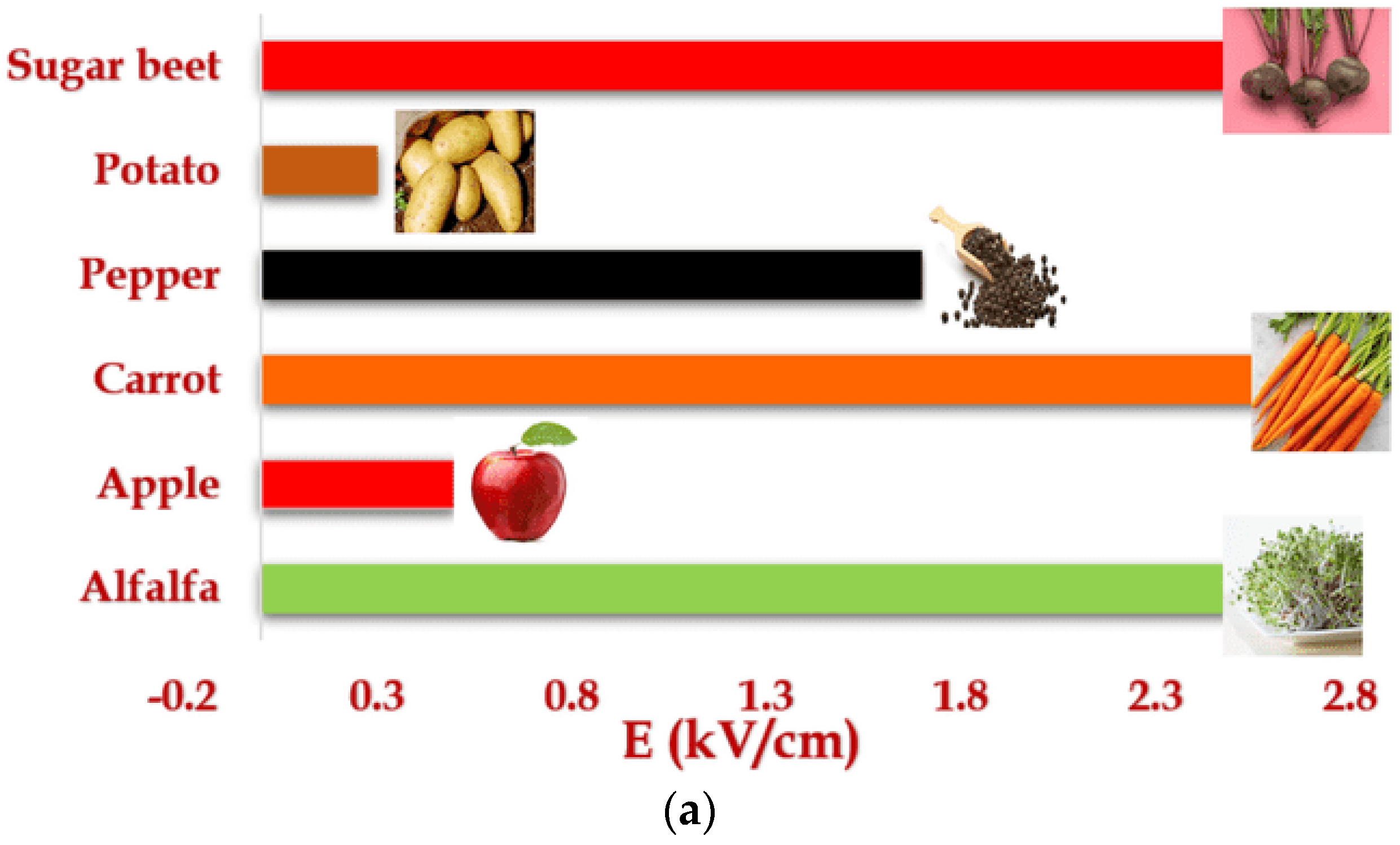
PEF(pulsed electric field)
[20,21]
  • Short duration pulses applied on short term leading to less energy usage and no heat generation
  • Not suitable for foods unable to withstand higher electric fields.
  • Well suited for liquid samples treatment.
There are converters developed widely with applications based on renewable energy though pertaining to higher efficiencies, control strategies and switching operations. Isolated and non-isolated converters are the two main divisions of DC converters. When developing isolated DC converters, a high-frequency transformer is utilized to create an electrical isolation amid the converter’s input and output. Despite having a programmable positive or negative polarity for the converter’s output and being intended to safeguard sensitive loads, this feature has a severe noise interference characteristic. Table 1 gives the comparison of the PEF method of food processing with the other non-thermal methods adapted in the food processing industry to show its superiority over other non-thermal methods of food processing.
Minimum pulsed electric field voltages in the range of 0.3 kV–5 kV is effective in food processing [24,25,26,27,28,29,30] which implies that even a conventional single stage boost converter output without multiplier stages can be employed in food preservation directly. The low voltage produced by the DC–DC generators generally needs high gain DC–DC converters to meet the requirements of the DC load [31,32]. Other than the conversion of renewable energy, DC–DC converters are used in varied applications such as uninterrupted power supply backup systems, discharge lamps of high intensity for head lamps in automobiles and some equipment in electric traction [33,34,35,36,37].Generally, the voltage stress posed on switches is equal to the output voltage in the high boost DC–DC converters conventionally used in recent years. However, to meet the stress due to high voltage, switches are selected with higher voltage ratings, resulting in high conduction loss. Also, the selection of high duty ratio switches also results in high voltage spikes, increased conduction loss and serious reverse recovery problems in diodes [38,39,40]. The desired high voltage gain can be achieved from various DC–DC isolated converter topologies proposed in the literature [41,42,43]. Saturation of the core is the problem in this type of isolated converter. Moreover, the introduced leakage inductance by the coupled inductors and transformers necessitates the need for a snubber circuit [41], voltage-clamp diode [42] and active-clamp circuit [43,44].
DC–DC converters of the non-isolated type are therefore used where the galvanized isolation is not in need. A high voltage gain is also achieved with a reduced cost and size. Quadratic boost [45], voltage shift [46], capacitor-diode voltage multiplier [47], switched-inductor and switched capacitor [48] based boost converters are some of the non-isolated boost topologies with high gain. The efficiency of a boost converter can be increased in many ways. The cascading of converter stages can increase the voltage gain. An issue of instability and control circuit complexity occurs due to an increase in the component count in cascaded cycling [49]. The gain can be increased by increasing the number of switched inductor and switched capacitor cells. Though there is an increase in the component count in this combination of switched inductor and switched capacitor, they have their own advantages. The leakage reactance stored energy can be absorbed by switched capacitors. No additional snubber circuit is required. To reduce conduction loss, MOSFET with low on-state resistor is suggested for selection [50]. A suitable converter topology efficiently boosting a low input voltage to a high output bus voltage is discussed and experimentally verified in [51,52]. To alleviate the reverse recovery problems and stress on diodes, Schottky diodes are used and a prototype designed for 40 W is experimentally verified for the converter performance [53]. With a simple topology, a high output voltage obtained with a low duty ratio can be easily obtained just by increasing the number of inductor cells of the circuit topology. The results are analyzed experimentally [54]. Another topology, applying the same gating pulses for the two switches, is proposed efficiently to obtain a high conversion ratio with a reduced loss on the converter and experimentally validated [20,21,22,23,55,56,57,58,59].
Substantial attention has been drawn over the past few years by high step ratio dc–dc converters due to their wide range of utilization. In this paper, a new improved converter is presented with an appreciable voltage gain for PEF. It is fed from an isolated DC source of low voltage with a switching inductor (SL) cell and switching capacitor (SC) cell. The output stage of the configuration has a high voltage switch which in turn stands as the main disadvantage of the circuit owing to its high voltage chopping functionality and capacity in turn. High voltage unipolar pulses are produced by the chopping of DC voltage elevated by the high voltage switch. The gain can be increased to a very high value by increasing the number of SL and SC cells.
The advantages of the proposed converters are as follows:
(i)
Single switch topology;
(ii)
Scalable;
(iii)
Regulated output voltage;
(iv)
High efficiency;
(v)
Less stress on semiconductor devices;
(vi)
High voltage output.
The above advantages are verified suitably using simulation results, mathematical derivations and a prototype. The simulation and hardware specifications are tabulated and the results are provided in the following sections.

2. Passive Switched Inductor Switched Capacitor (PSLSC) Converter

The boosted voltage level is achieved by combining a switched inductor cell and a switched capacitor cell, as shown in Figure 2a,b. The boost converter proposed is a combination of switched inductor and switched capacitor cells, as shown in Figure 2c. The proposed converter comprises of a dynamic switch (SW), an output capacitor (C0), output inductor (L0), load resistance (RL), a switched inductor cell and a switched capacitor (SC) cell.

3. PSLSC Converter CCM Analysis

In this segment, the operating principle of a PSLSC converter with a SL and SC cell is discussed. The proposed converter shown in Figure 3 is effective in food processing applications. Figure 3 depicts the circuit of the PSLSC converter and further analysis will be carried out with this circuit. The switched inductor (SL) cell consists of two diodes (DSL1 and DSL2), an inductor (L and LSL1) and a capacitor (CSL1). The SC cell consists of two diodes (DSC1 and DSC2) and two capacitors (CSC1 and CSC2). The SL cell charges during the ON period and discharges to the load during the OFF condition of the dynamic switch.

3.1. Operating Modes of Converter Proposed in CCM

Mode 1:
The switch ‘SW’ conducts at t = t0. Diodes DSL1 and DSL2 are forward biased. The inductors ‘L’ and ‘LSL1’ are excited by the input DC source Vg. The inductors ‘L’ and ‘LSL1’ are connected in parallel with capacitor CSL1. The DC energy source is transferred to the inductor ‘L’. The current Ig is equal to the accumulation of the currents IL, ILSL1 and ICSL1. The capacitors CSC1 and CSC2 are connected in series with inductors L0 as the two diodes DSC1 and DSC2 are reverse biased and supply the load resistance RL. Figure 4 shows the flow of current in the converter circuit during this interval.
Considering the ‘ON’ stage of the switch ‘SW’ in the main circuit and applying the principle of inductor voltage-second balance, the following equations are obtained:
0 DT s V L dt = 0 DT s V SL 1 dt   = 0 DT s V CSL 1 dt   = 0 DT s V g dt
0 DT s V LO dt = 0 DT s ( 2 V CSC 1 V 0 ) dt  
On the application of the principle of capacitor current-second balance to the main circuit while the switch ‘SW’ is in ON state, the following relationships are obtained:
0 DT s I CSL 1 dt = 0 DT s I g 3   dt
0 DT s I CSC 1 dt = 0 DT s I CSC 2 dt = 0 DT s I L 0 dt
0 DT s I C 0 dt = 0 DT s ( I L 0 I 0 ) dt
Mode 2:
During the instant the switch ‘SW’ is turned off, the inductor ‘L’ capacitor CSL1 and inductor LSL1 are connected in series as the diodes DSL1 and DSL2 are reverse biased. The diodes DSC1 and DSC2 are forward biased and they connect the capacitors CSC1 and CSC2 in parallel. This makes the voltage boosted to a high value and available across C0 and RL. The current flow path of the converter circuit during this interval is shown in Figure 5.
On the application of the principle of inductor voltage-second balance, to the PSLSC circuit while the switch ‘SW’ is in OFF state, the following relationships are obtained:
DT s T s V L dt = DT s T s ( V g V CSC 1 ) 3 dt = DT s T s VL SL 1   dt  
DT s T s V L 0 dt = DT s T s ( V CSC 1 V CO ) dt  
On the application of the principle of capacitor current-second balance to the PSLSC circuit while the switch ‘SW’ is in OFF state, the following relationships are obtained:
DT s T s I CSL 1 dt = DT s T s I L dt  
DT s T s I CSC 1 dt = DT s T s I CSC 2 dt = DT s T s I L I L 0 2 dt  
DT s T s I C 0 dt = DT s T s ( I L O I 0 ) d t

3.2. Derivation of PSLSC Converter Voltage Gain

The waveforms related to the voltage and the current of active and passive components of the PSLSC converter in CCM mode are given in Figure 5. On simplifying (1), (2), (6) and (7) the following voltage equations are obtained.
V CSL 1 = V g  
V CSC 1 = V CSC 2 = V g   ( 1 + 2 D ) ( 1 D )
The voltage gain ratio of PSLSC converter is
V 0 V g = ( 1 + 2 D ) ( 1 + D ) ( 1 D )
On simplifying (3), (4), (5), (8), (9) and (10) the following current equations are obtained.
I L = I LSL 1 = I 0 ( 1 + D ) 1 D
I LO = I O
Equation (13) is the voltage ratio of the proposed converter. When the numbers of SL and SC cells are increased, the gain of the converter increases. The increase in the number of switched inductor cell increases the voltage ratio and makes no change with respect to the gain ratio with respect to odd (or) even numbers of switched inductor cells. Whereas the addition of switched capacitor cells in odd (or) even numbers makes considerable changes of the voltage boost ratio. The generalized voltage boost ratio with ‘M’ number of cells added is given below.
G V ( M = 1 , 3 , 5 , .. ) = V 0 V g = [ 1 + 2 M SL D ] [ M SC + D ] [ 1 D ]
G V ( M = 2 , 4 , 6 , .. ) = V 0 V g = [ 1 + 2 M SL D ] [ M SC + 1 ] D ] [ 1 D ]
The proposed topology waveforms are given in Figure 6a,b. Figure 6a shows the wave forms of voltages depicting the gate pulse of switch ‘SW’, VCSL1, VDSL1, VDSL2, VCSC1, VCSC2 and VSW from top to bottom. Figure 6b shows the wave forms of currents that are related to gate pulse of switch ‘SW’, ILSC1, IL0, Vg and VOUT from topmost to bottom.
A correlation table is made with the increase in odd and even number of switched inductor and switched capacitor cells and is shown in Table 2 and Table 3.
It is observed from Table 2 and Table 3 that the increase in switched capacitor cells gives more gain when compared with the gain obtained with an increase in switched inductor cells. The increase in odd or even numbers of switched capacitor cells poses no change in switch stress in terms of Vg as can be found from Table 3. Increase in number of switched capacitors further decreases the switch stress in terms of V0. The voltage stress on switch in terms of V0 remains constant irrespective of the increase in switched inductor cells in odd (or) even numbers as can be observed from Table 2. The voltage stress on the switch in terms of Vg is considerably high with an increase in the number of cells of the switched inductor. A proper selection of MSC and MSL can give a very high voltage gain suitable for the generation of high voltage pulses with minimal stress on the switch.

4. Analysis of PSLSC Converter in DCM (Discontinuous Conduction Mode)

When a converter is designed for an application, it is necessary to study the operation of the converter in DCM and BCM conditions. This section elaborates on the operation of the proposed PSLSC converter in discontinuous conduction.
Figure 7b shows the current flow in inductor during D1TS, D2TS and D3TS. The average current through the inductor L0 is found. From Figure 7a, the current in inductor is obtained as
i L 0 ( t ) = i C 0 ( t ) + v ( t ) R 0
Average   current = i L 0 = 1 T 0 T S i L 0 ( t ) d t = V 0 R 0
The area of the triangle also gives the average current through the inductor L0.
Area   of   Triangle = 1 2 [ 2 V C V 0 L 0 ] D 1 T S [ D 1 + D 2 ]
Equating (19) and (20), the (21) is obtained.
V 0 R 0 = 1 2 [ 2 V g V 0 L 0 ] D 1   T S [ D 1 + D 2 ]
Considering Figure 7b, the gain of the converter is determined. The volt-second balance expression in ON mode is obtained as
V g D 1 T S + ( V g V C ) 3 D 2 T S = 0
Simplifying (22), the following expression is obtained as
V C = [ 1 + 3 D 1 D 2 ] V g
Similarly, the volt-second balance law is applied on the non-conducting period of the converter in DCM mode and the obtained expression is
2 V C D 1 V 0 D 1 + V C D 2 V 0 D 2 = 0
After simplifying the gain of the converter under DCM is given as
V 0 = [ 1 + 3 D 1 D 2 ] [ 2 D 1 + D 2 D 1 + D 2 ] V g
where K = 2 L 0 R 0 T S .

5. Analysis of PSLSC Converter Topology in BCM (Boundary Conduction Mode)

The boundary between CCM and DCM is BCM. While the converter proposed operates in BCM, the gain of CCM and DCM are equal. The critical value of ‘K’ obtained is given in Equation (29). Figure 8 shows the curve of ‘Kcrit’ in terms of ‘D’. At the boundary of DCM and CCM, the converter operates in a condition where K=Kcrit. When K>Kcrit, the converter functions in CCM ( I L > i L ) and when K<Kcrit the converter functions in DCM ( I L < i L ) .
The inductor current ripple is given as
i L = i L S L 1 = V g D T S 2 L
Considering the operation of the converter at the boundary condition
I 0 ( 1 + D ) 1 D > V g D T S 2 L
On substituting (26) in (27) and rearranging the Kcrit value is obtained as
2 L f s R 0 > ( 1 D ) D G V C C M
K c r i t ( D ) = D ( 1 D ) G V C C M
From Figure 8 it is observed that at D = 0.2, the value of Kcrit is 0.07619. When K > 0.07619, the PSLSC functions in CCM and when K < 0.07619 it functions in DCM.

6. Design of PSLSC Converter and Stress Analysis

a 
Inductors Design
The input inductor ‘L’ of the converter proposed is calculated in the CCM as follows:
L = R L   ( 1 D ) 2 D 2 ( 2 D 2 + 3 D + 1 ) ( 1 + D ) f s
The inductor of switched inductor cell is found to be same as that of input inductor. It is expressed as
L S L 1   = R L   ( 1 D ) 2 D 2 ( 2 D 2 + 3 D + 1 ) ( 1 + D ) f s
whereas the fs represents the switching frequency and R0 is the load resistance. The input inductor is also a function of frequency, load resistance and duty ratio. It is expressed as
L 0 = R L ( 1 D ) D 2 ( 1 + D ) f s
b 
Capacitor Design
The average current passing through the capacitors during their conduction period is considered and the relationship of the capacitors is obtained as follows using the Equations (11) and (12). The ripple voltage is considered as 10% of the capacitor voltage. The various capacitor expressions are as follows:
C S L 1 = ( 2 D 2 + 3 D + 1 ) I 0 D V c S L 1 f s ( 1 D )
C S C 1 = C S C 2 = I 0 D V C S C 1 f s
C 0 = I 0 D V C 0 f s
c 
PSLSC converter Switch Stresses
Based on the analysis of the PSLSC converter in CCM, the switch stresses on the components are calculated and tabulated in Table 4. The parasitic factors are ignored for the convenience of calculating the voltage current stress. All the stress depends on the duty ratio and by the proper selection of the duty ratio the efficiency can be maintained high with nominal stress on the components.

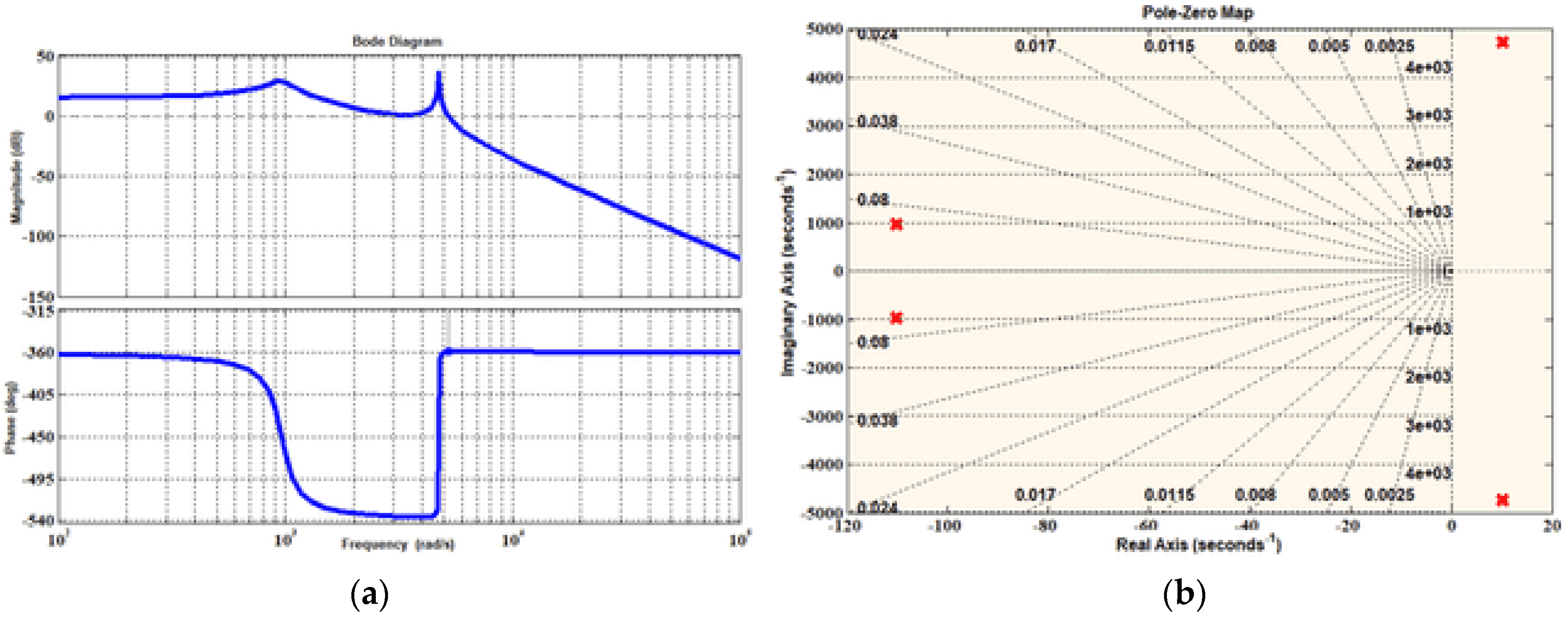
7. Dynamic Analysis of PSLSC Converter

The state space equations are used to obtain a piecewise linear model in order to describe the behavior of the converter proposed. State space equations are obtained resulting in electrical trajectories, owing to the turn ON/OFF conditions of switch and diodes. Vg and V0 are the input and output variables, respectively. The inductor currents iL, iLSL1 and iL0 and capacitor voltages VCSL1, VCSC1, VCSC2 and VC0 form the variables of the state space equations. The inductors L and LSL1 are selected to be of the same value while all the capacitors in the circuit are selected to be of the same value. The same value components usage results in same voltage and current across them when they are connected in series and parallel with respect to the ON/OFF condition of the switch. The inductor currents and capacitor voltages are treated as single variable with the assumption that there is no generality loss. From Figure 5, it can be observed that the inductors L and LSL1 are in series and capacitors CSC1, CSC2 and C0 are in parallel, which means the currents through L and LSL1 are equal and the voltages of CSC1, CSC2 and C0 are same. Therefore, the state variables VCSC1, VCSC2 and iLSL1 are invalid, while the state variables iL, iL0, VC and VC0 are considered. Similarly, the voltages in capacitors CSC1, CSC2 and C0 are equal and the currents through L and LSL1 are equal as shown in Figure 4. The state variables VCSC1, VCSC2 and iLSL1 are invalid, the variables iL, iL0, VC and VC0 are considered. The PSLSC system is represented in a steady state with state variables iL, iL0, VC and VC0 and the input-output variables Vg and V0.
The steady-state representation of a system in general is given by
x ( t ) ˙ = A x ( t ) + B u ( t )
y ( t ) = C x ( t ) + D u ( t )
During the ON and OFF conditions, the state equation of the system in general form is given as follows:
x ( t ) ˙ = A 1 x ( t ) + B 1 u ( t )
y ( t ) = C 1 x ( t ) + D 1 u ( t )
x ( t ) ˙ = A 2 x ( t ) + B 2 u ( t )
y ( t ) = C 2 x ( t ) + D 2 u ( t )
The proposed PSLSC converter state equations during the ON and OFF conditions are given as follows:
During ‘ON’ condition of the switch
[ i L ˙ i L 0 ˙ v C ˙ v C 0 ˙ ] = [ 0 0 0 0 0 0 2 L 0 1 L 0 0 1 C 0 0 0 1 C 0 0 1 R L C 0 ] [ i L i L 0 v C v C 0 ] + [ 1 L 0 0 0 ] [ v g ]
during ‘OFF ‘condition of the switch
[ i L ˙ i L 0 ˙ v C ˙ v C 0 ˙ ] = [ 0 0 1 3 L 0 0 0 1 L 0 1 L 0 1 2 C 1 2 C 0 0 0 1 C 0 0 1 R L C 0 ] [ i L i L 0 v C v C 0 ] + [ 1 3 L 0 0 0 ] [ v g ]
the output voltage is given as
[ V 0 ] = [ 0 0 0 0 ] [ i L i L 0 v C v C 0 ] + [ 0 ] [ v g ]
The generalized input to output transfer function is given as
V 0 ( S ) V g ( S ) = C [ S I A ] 1 B
On substituting the values for A, B, C and D matrices, the gain expression under dynamic analysis is as follows:
V 0 ( S ) V g ( S ) = [ 0 0 0 1 ] [ [ S 0 0 0 0 S 0 0 0 0 S 0 0 0 0 S ] [ 0 0 D 3 L 0 0 0 1 + D L 0 1 L 0 D 2 C ( 1 + D ) 2 C 0 0 0 1 C 0 0 1 R 0 C 0 ] ] 1 . [ 1 + 2 D 3 L 0 0 0 ]
where
A = [ 0 0 D 3 L 0 0 0 1 + D L 0 1 L 0 D 2 C ( 1 + D ) 2 C 0 0 0 1 C 0 0 1 R 0 C 0 ]
B = [ 1 + 2 D 3 L 0 0 0 ]
C = [ 0 0 0 1 ]
D = [ 0 ]
By simplifying and rearranging, the input to output transfer function is obtained as
V 0 ( s ) V g ( s ) = ( 1 D ) ( 1 + 2 D ) D 6 L L 0 C C 0 S 4 6 L L 0 C C 0 R 0 + S 3 6 L L 0 C + S 2 [ D 2 L 0 C 0 R 0 + ( 1 + D ) 2 3 L C 0 R 0 + 6 L C R 0 ] + S [ D 2 L 0 + ( 1 + D ) 2 6 L ] + R 0 D 2 6 L L 0 C C 0 R 0
On further simplification, the transfer function of the PSLSC converter is finally obtained as
V 0 ( S ) V g ( S ) = ( 1 + 2 D ) ( 1 + D ) ( 1 D ) [ 1 + S [ L 0 R 0 + 6 ( 1 + D ) 2 L D 2 R 0 ] + S 2 [ L 0 C 0 + 3 L C 0 ( 1 + D ) 2 D 2 + 6 L C D 2 ] + S 3 6 L L 0 C D 2 R 0 + S 4 6 L L 0 C C 0 D 2 ]
The transfer function in Equation (52) is used to design the voltage feedback compensation. To determine the stability of the system, the following parameters are used. Vg = 300 V, Vo = 1.8 kV, Ro = 500 Ω, D = 0.5 and fs = 50 kHz. The reason for this operating voltage for the proposed converter is that the converter is designed for food processing applications. The power rating of this application is around 50–100 W. The bode plot and pole-zero map of the transfer function given in Equation (52) is given in Figure 9. It can be found from the plot and map that the system is not stable and the selection of a suitable converter can make the system stable. Red cross denotes the poles in the map.

8. Efficiency Analysis

This section discusses the proposed converter efficiency. Figure 10 shows the equivalent circuit of the proposed converter. The internal resistances of the diodes DSL1, DSL2, DSC1 and DSC2 are represented as RfDSL1, RfDSL2, RfDSC1 and RfDSC2, respectively. The ESR of the inductors L, LSL1 and L0 are represented as RL, RLSL1 and RL0. Similarly, ESR of capacitors CSL1, CSC1, CSC2 and C0 are represented as RCSL, RCSC1, RCSC2 and RC0, respectively. The ‘ON’ state resistance of the switch is denoted as RSW.
The power loss on the switch is denoted as PSW and it is given as
P S W = P S W ( c o n d u c t i o n ) + P S W ( s w i t c h i n g )
P S W ( c o n d u c t i o n ) = I 0 2 ( 1 + 2 D ) 2 ( 1 + D ) 2 D R D S ( o n ) ( 1 D ) 2
P S W ( s w i t c h i n g ) = f s C 0 V m a x 2 2       = f s C 0 V g 2 ( 1 + 2 D ) 2 2 ( 1 D ) 2
The power losses on the diodes are given as PD and PD as follows:
P D = 2 I 0 ( 1 + 2 D ) ( 1 + D ) D V F   3 ( 1 D ) + 4 I 0   D V F   + 2 I 0 2 ( 1 + D ) 2 ( 1 + 2 D ) 2 9 ( 1 D ) 2 D R F +   4 I 0 2 D 2 1 D R F
PL and PC denotes the inductor and capacitor loss and is given as
P L = 2 [ I 0   ( 1 + D ) ] 2 R L ( 1 D ) 2     + I 0 2 R L
P C = [ I 0 2 ( 1 + 2 D ) 2 ( 1 + D ) 2 ( 3 2 D ) ( 1 + D ) D V F   3 ( 1 D ) 2   + 2 I 0 2 D ( 1 D ) +   I 0 2   D ] R C
The total power loss (PLOSS) in the converter is given as
P L O S S = P S W + P D + P L + P C
The efficiency ( η )   of the proposed high step-up converter is given by
E f f i c i e n c y = η = P 0 P i n = 1 1 + ( P L O S S P 0 )

9. Comparative Study

Table 5 presents the comparison of the proposed converter and other DC–DC converters developed recently in terms of voltage gain, component count, extendibility and switch count. Figure 11 demonstrates the voltage ratio versus the duty cycle for the converters in [51,52,53,54,55,56]. It is clear that the boost ratio of the converter PSLSC is higher when compared with the converters in [52,53,54,55,56]. This characteristic feature makes the converter PSLSC much more suitable for step-up application in a higher range. At the expense of a higher component quantity, the converters [51,52,53,54,55,56] are shown to have a high voltage gain compared with the proposed topology. For instance, the [53] has a single switch topology as that of the proposed one but the extendibility and boost ratio is less when compared with the proposed converter. Though a converter [54] offers extendibility, it has more switch counts and switch stresses than the PSLSC converter.
Table 5. Comparison of PSLSC converter and existing high gain converters.
ConverterVoltage GainComponent CountExtendableSingle Switch Topology
SwDLC
Proposed converter ( 1 + 2 M S L D ) ( 1 + M S C D ) 1 D 12(MSL + MSc)MSL + 21 + MSL + 2MScYes
APIC converter [54] 1 + ( n + 1 ) D 1 D n + 22nn + 21YesX
ASLPSC converter [55] 1 + 3 D 1 D 2233NoX
Modified sepic [52] 1 + 3 D 1 D 2233NoX
SH-SLC converter [56] 1 + 3 D 1 D 2741NoX
Switched inductor [51] 3 D 1 D 2323NoX
Boost with VM cell [53] 2 + D 1 D 1425No

10. Simulation Results

A simulation circuit is designed with the rating of 65 W and 1.8 kV output voltages. From the Expressions (34)–(39), the values of inductors and capacitors are calculated as given in Table 6. Table 6 gives the chosen design specifications of the proposed converter. This simulation analysis is performed to validate that the PSLSC converter is suitable for pulsed electric field (PEF) in the food industry. For vegetable tissue drying, the required pulsed electric field is 0.5–5 kV/cm. In this aspect, we have assumed the distance between the electrode as 1 cm and the area of the plate as 1 cm2. With these specifications, the equivalent resistance of the sample to be dried is calculated as 500 Ω (1 cm/(2000 µs/cm × 1 cm2)).
The simulation is carried out in an nl5 simulator. The reason for choosing the output voltage of the converter as 1.8 kV is illustrated in Figure 11a. For vegetable and fruit juice expression and tissue drying, the required high voltage pulses ranges from 0.3 to 5 kV. Figure 11b shows the simulation circuit with the design values of each of the components exactly as used in the simulator. The obtained output voltage, switch and diodes’ stress in terms of voltage are given in Figure 11c–f.
Figure 11e presents the regulated voltage obtained from the PSLSC converter with 300 V input voltage and a gain of six. A high voltage switch is used to chop this regulated dc voltage with a 10% duty cycle and a switching frequency of 1 kHz. The repetitive high voltage pulse is presented in Figure 11f.
Table 7 presents the comparative result which depicts the validation of theoretical study with the simulation results. From this table, it is clear that the voltage rating of the components in the converter is lesser than the output voltage with the single SL and SC cells. In this case, if the SL and SC cells are extended to generate high voltage pulses then the voltage rating of the components will be further reduced due to the division of the voltage in the components. The efficiency of the converter is noted to be 93% for this rating. Figure 12 shows the comparison of the proposed PSLSC converter with the converters in [33,58] to highlight the advantage of the converter.

11. Experimental Results

The proposed PSLSC converter is tested for its design effectiveness for a 10 V input voltage and a 42 V output with 50 W to verify the theoretical analysis in CCM mode of the operation. The list of hardware components taken for the construction of prototype is given in Table 8. The prototype is scaled down and tested to confirm the potential ability of the proposed PSLSC high voltage pulse generator. The photograph of the experimental setup with the results obtained is presented in Figure 13a–h. the pulse generator is fed with the input voltage of 10 V and it operates with the duty cycle of 0.4 to generate the output voltage of 42 V. Pulsed output voltage is obtained with a 10-microsecond pulse width and the obtained data are presented in Figure 13b.
From the results obtained from the prototype, it is more obvious that the scaled down prototype generates the desired voltage required for the mentioned application. It generates the pulse with the width of 10 µs and a repetition rate of 500 per second. The operation of switched inductor cell is validated with the results obtained across the L and LSL1. This is verified with the results illustrated in Figure 13e,f. These two inductors are parallelly charged and discharged serially at the ON and OFF conditions of the switch.

12. Conclusions

In this paper, a high voltage pulse generator is proposed for food processing which can be used for mechanical extraction, solid-liquid extraction, dehydration, freezing, etc. The design steps involved in this topology are presented. Steady-state and dynamic study is performed in a continuous conduction mode and the necessary waveforms are presented. It is noted that the topology has an attractive feature of extendable capability for increasing the voltage gain. This topology is also more suitable to domestic use if it is presented with multiple SL and SC cells and it can be integrated with the available standard voltage source in the domestic location. Furthermore, the converter can employ lower rating components with the integration of multiple cells with the feature of extendibility. This feature allows us to generate high voltages in a kV range with low voltage components. To meet up to the high voltage need of practical food processing applications, the number of multiplier stages need to be increased. This increases the number of components, cost and thereby the weight of the converter. However, the operation of the circuit is simple as it is a single switch topology. High rated switches need to be selected when the numbers of converter stages are increased for higher voltage applications and operations.
Dynamic study is performed using state–space analysis and the inference from the frequency response is discussed. The efficiency of the converter is observed to be 93%. A simulation study is performed with 1.8 kV, 65 W rating to generate a repetitive high voltage pulse at 500 pulses/second with a 100 µsec pulse width. Finally, a scaled down prototype is tested with a 50 W rating and the repetitive pulse is obtained with 42 V. The way to perform the MPPT action for the proposed converter is the future scope.

Author Contributions

Conceptualization, P.S., J.D.N., A.L. and J.S.; methodology, J.D.N., P.S.; software, J.D.N. and A.L.; validation, J.D.N. and P.S.; formal analysis, A.L., R.Z., F.A.E. and J.S.; investigation, J.D.N., R.Z. and F.A.E.; resources, P.S., J.D.N., A.L. and J.S.; data curation, J.D.N., A.L. and J.S.; writing—original draft preparation, J.D.N., R.Z., F.A.E. and A.L.; writing—review and editing, P.S. and J.D.N.; supervision, J.D.N.; project administration, J.D.N. All authors have read and agreed to the published version of the manuscript.

Funding

This research received no external funding.

Data Availability Statement

All data generated or analyzed during this study are included in this article.

Conflicts of Interest

The authors declare no conflict of interest.

Abbreviations

VgInput Voltage
VOOutput Voltage
VLInductor Voltage
VCCapacitor Voltage
ΔVCCapacitor Voltage Ripple
ΔILInductor Current Ripple
RLLoad Resistance
DDuty Ratio
PinInput Power
POOutput Power
PLOSSPower Loss
PSWPower Loss on switch
PDPower Loss on diode
PLPower Loss on inductor
PCPower Loss on capacitor
SCSwitched capacitor
SLSwitched inductor
RfDSL1, RfDSL2, RfDSC1, RfDSC2Parasitic resistance of inductor
RLSL1,RL1, RL0Parasitic resistance of capacitors
RCSC1, RCSC2, R0Parasitic resistance of diodes
HEfficiency

References

  1. Niu, D.; Zeng, X.-A.; Ren, E.-F.; Xu, F.-Y.; Li, J.; Wang, M.-S.; Wang, R. Review of the application of pulsed electric fields (PEF) technology for food processing in China. Food Res. Int. 2020, 137, 109715. [Google Scholar] [CrossRef]
  2. Pataro, G.; Falcone, M.; Donsì, G.; Ferrari, G. Metal release from stainless steel electrodes of a PEF treatment chamber: Effects of electrical parameters and food composition. Innov. Food Sci. Emerg. Technol. 2014, 21, 58–65. [Google Scholar] [CrossRef]
  3. Syed, A.I.Q.A.; Rahman, S.A.U.U.; Shukat, R. Pulsed Electric Field Technology in Food Preservation: A Review. J. Nutr. Health Food Eng. 2017, 6, 168–172. [Google Scholar] [CrossRef] [Green Version]
  4. Ricci, A.; Parpinello, G.P.; Versari, A. Recent Advances and Applications of Pulsed Electric Fields (PEF) to Improve Polyphenol Extraction and Color Release during Red Winemaking. Beverages 2018, 4, 18. [Google Scholar] [CrossRef] [Green Version]
  5. Kirawanich, P.; Satusap, P.; Chavasit, V.; Islam, N.E. Microorganism Inactivation by Nano second Pulsed Electric Fields: Full-wave Analysis and Experiment. In Proceedings of the International Conference on Food Engineering and Biotechnology, Bangkok, Thailand, 7–9 May 2011. [Google Scholar]
  6. Dastgheib, A.M.; Buntat, Z.; Sidik, M.A.B. Chemical Analysis on the Effect of Pulsed Electric Fields in Pineapple Juices Preservation. Appl. Mech. Mater. 2014, 554, 588–592. [Google Scholar] [CrossRef]
  7. Noci, F.; Riener, J.; Walkling-Ribeiro, M.; Cronin, D.; Morgan, D.; Lyng, J. Ultraviolet irradiation and pulsed electric fields (PEF) in a hurdle strategy for the preservation of fresh apple Juice. J. Food Eng. 2008, 85, 141–146. [Google Scholar] [CrossRef]
  8. Pataro, G.; Carullo, D.; Siddique, M.A.B.; Falcone, M.; Donsì, F.; Ferrari, G. Improved extractability of carotenoids from tomato peels as side benefits of PEF treatment of tomato fruit for more energy-efficient steam-assisted peeling. J. Food Eng. 2018, 233, 65–73. [Google Scholar] [CrossRef]
  9. Timmermans, R.; Mastwijk, H.; Berendsen, L.; Nederhoff, A.; Matser, A.; Van Boekel, M.; Groot, M.N. Moderate intensity Pulsed Electric Fields (PEF) as alternative mild preservation technology for fruit juice. Int. J. Food Microbiol. 2019, 298, 63–73. [Google Scholar] [CrossRef]
  10. Tylewicz, U.; Tappi, S.; Genovese, J.; Mozzon, M.; Rocculi, P. Metabolic response of organic strawberries and kiwifruit subjected to PEF assisted-osmotic dehydration. Innov. Food Sci. Emerg. Technol. 2019, 56, 102190. [Google Scholar] [CrossRef]
  11. Evrendilek, G.A.; Agcam, E.; Akyildiz, A. Effects of pulsed electric fields on sour cherry juice properties and formations of furfural and hydroxymethylfurfural. Int. J. Food Eng. 2020, 17, 217–226. [Google Scholar] [CrossRef]
  12. Ribas-Agustí, A.; Martín-Belloso, O.; Soliva-Fortuny, R.; Elez-Martínez, P. Influence of pulsed electric fields processing on the bioaccessible and non-bioaccessible fractions of apple phenolic compounds. J. Funct. Foods 2019, 59, 206–214. [Google Scholar] [CrossRef]
  13. Velickova, E.; Tylewicz, U.; Rosa, M.D.; Winkelhausen, E.; Kuzmanova, S.; Romani, S. Effect of pulsed electric field coupled with vacuum infusion on quality parameters of frozen/thawed strawberries. J. Food Eng. 2018, 233, 57–64. [Google Scholar] [CrossRef]
  14. Taiwo, K.A.; Eshtiaghi, M.N.; Ade-Omowaye, B.I.; Knorr, D. Osmotic dehydration of strawberry halves: Influence of osmotic agents and pretreatment methods on mass transfer and product characteristics. Int. J. Food Sci. Technol. 2003, 38, 693–707. [Google Scholar] [CrossRef]
  15. Angersbach, A.; Knorr, D. High intensity electric field pulses as pretreatment for affecting dehydration characteristics and rehydration properties of potato cubes. Nahrung-Food 1997, 41, 194–200. [Google Scholar] [CrossRef]
  16. Ade-Omowaye, B.I.O.; Rastogi, N.K.; Angersbach, A.; Knorr, D. Combined effects of pulsed electric field pre-treatment and partial osmotic dehydration on air drying behaviour of red bell pepper. J. Food Eng. 2003, 60, 89–98. [Google Scholar] [CrossRef]
  17. Tedjo, W.; Taiwo, K.A.; Eshtiaghi, M.N.; Knorr, D. Comparison of pretreatment methods on water and solid diffusion kinetics of osmotically dehydrated mangos. J. Food Eng. 2002, 53, 133–142. [Google Scholar] [CrossRef]
  18. Taiwo, K.A.; Angersbach, A.; Ade-Omowaye, B.I.O.; Knorr, D. Effects of pretreatments on the diffusion kinetics and some quality parameters of osmotically dehydrated apple slices. J. Agric. Food Chem. 2001, 49, 2804–2811. [Google Scholar] [CrossRef]
  19. Rastogi, N.K.; Eshtiaghi, M.N.; Knorr, D. Accelerated mass transfer during osmotic dehydration of high intensity electrical field pulse pretreated carrots. J. Food Sci. 1999, 64, 1020–1023. [Google Scholar] [CrossRef]
  20. Kasri, N.F.; Piah, M.A.M.; Adzis, Z. Compact High-Voltage Pulse Generator for Pulsed Electric Field Applications: Lab-Scale Development. J. Electr. Comput. Eng. 2020, 2020, 6525483. [Google Scholar] [CrossRef]
  21. Song, H.-J.; Lee, J.-H.; Bin Song, K. Effects of irradiation and fumaric acid treatment on the inactivation of Listeria monocytogenes and Salmonella typhimurium inoculated on sliced ham. Radiat. Phys. Chem. 2011, 80, 1291–1293. [Google Scholar] [CrossRef]
  22. Navamani, J.D.; Lavanya, A.; Vijayakumar, K. Modified SEPIC converter with high boosting capability. Electron. Lett. 2019, 55, 759–761. [Google Scholar] [CrossRef]
  23. Kumar, Y.; Patel, K.; Kumar, V. Pulsed Electric Field Processing in FoodTechnology. Int. J. Eng. Stud. Tech. Approach 2015, 1, 6–17. [Google Scholar]
  24. Shtiaghi, M.N.; Knorr, D. High electric field pulse pretreatment: Potential for sugar beet processing. J. Food Eng. 2002, 52, 265–272. [Google Scholar] [CrossRef]
  25. Lebovka, N.I.; Praporscic, L.; Vorobiev, E. Enhanced expression of juice from soft vegetable tissues by pulsed electric fields: Consolidation stages analysis. J. Food Eng. 2003, 59, 309–317. [Google Scholar] [CrossRef]
  26. Ade-Omowaye, B.I.O.; Angersbach, A.; Eshtiaghi, N.M.; Knorr, D. Impact of high intensity electric field pulses on cell permeabilisation and as pre-processing step in coconut processing. Innov. Food Sci. Emerg. 2001, 1, 203–209. [Google Scholar] [CrossRef]
  27. Ade-Omowaye, B.I.O.; Angersbach, A.; Taiwo, K.A.; Knorr, D. The use of pulsed electric fields in producing juice from paprika (Capsicum annuum L.). J. Food Process. Preserv. 2001, 25, 353–365. [Google Scholar] [CrossRef]
  28. Knorr, D.; Geulen, M.; Grahl, T.; Sitzmann, W. Food application of high-electric-field pulses. Trends Food Sci. Technol. 1994, 5, 71–75. [Google Scholar] [CrossRef]
  29. Bazhal, M.I.; Lebovka, N.I.; Vorobiev, E. Pulsed electric field treatment of apple tissue during compression for juice extraction. J. Food Eng. 2001, 50, 129–139. [Google Scholar] [CrossRef]
  30. Gachovska, T.K.; Adedeji, A.A.; Ngadi, M.O. Influence of pulsed electric field energy on the damage degree in alfalfa tissue. J. Food Eng. 2009, 95, 558–563. [Google Scholar] [CrossRef]
  31. Forouzesh, M.; Siwakoti, Y.P.; Gorji, S.A.; Blaabjerg, F.; Lehman, B. Step-Up DC–DC Converters: A Comprehensive Review of Voltage-Boosting Techniques, Topologies, and Applications. IEEE Trans. Power Electron. 2017, 32, 9143–9178. [Google Scholar] [CrossRef]
  32. Bi, H.; Wang, P.; Che, Y. A Capacitor Clamped H-Type Boost DC-DC Converter with Wide Voltage-Gain Range for Fuel Cell Vehicles. IEEE Trans. Veh. Technol. 2019, 68, 276–290. [Google Scholar] [CrossRef]
  33. Yang, L.-S.; Liang, T.-J.; Chen, J.-F. Transformerless DC–DC Converters with High Step-Up Voltage Gain. IEEE Trans. Ind. Electron. 2009, 56, 3144–3152. [Google Scholar] [CrossRef]
  34. Aiswarya, T.M.; Prabhakar, M. An Efficient High Gain DC-DC Converter for Automotive Applications. Int. J. Power Electron. Drive Syst. 2015, 6, 242. [Google Scholar] [CrossRef]
  35. Sayed, K.; Almutairi, A.; Albagami, N.; Alrumayh, O.; Abo-Khalil, A.G.; Saleeb, H. A Review of DC-AC Converters for Electric Vehicle Applications. Energies 2022, 15, 1241. [Google Scholar] [CrossRef]
  36. Lopatkin, N.; Zinoviev, G.S.; Zotov, L.G. Bi-directional high-voltage DC-DC-converter for advanced railway locomotives. In Proceedings of the 2010 IEEE Energy Conversion Congress and Exposition, San Jose, CA, USA, 20–24 September 2010; pp. 1123–1128. [Google Scholar] [CrossRef]
  37. Al Sakka, M.; Van Mierlo, J.; Gualous, H. DC/DC Converters for Electric Vehicles; InTech: Rijeka, Croatia, 2011. [Google Scholar] [CrossRef] [Green Version]
  38. Shaneh, M.; Niroomand, M.; Adib, E. Non-isolated interleaved bidirectional DC–DC converter with high step voltage ratio and minimum number of switches. IET Power Electron. 2019, 12, 1510. [Google Scholar] [CrossRef]
  39. Pourfarzad, H.; Pourfarzad, H.; Saremi, M.; Saremi, M.; Jalilzadeh, T.; Jalilzadeh, T. An extended high-voltage-gain DC–DC converter with reduced voltage stress on switches/diodes. Electr. Eng. 2020, 102, 2435–2452. [Google Scholar] [CrossRef]
  40. Koç, Y.; Birbir, Y.; Bodur, H. Non-isolated high step-up DC/DC converters—An overview. Alex. Eng. J. 2021, 61, 1091–1132. [Google Scholar] [CrossRef]
  41. Mirzaei, A.; Rezvanyvardom, M. High voltage gain soft switching full bridge interleaved Flyback DC-DC converter for PV applications. Sol. Energy 2020, 196, 217–227. [Google Scholar] [CrossRef]
  42. Tom, D.; Balapattabi, S. Coupled-inductor based high gain dc-dc converter. Int. J. Technol. Res. Eng. 2015, 2, 2347–4718. [Google Scholar]
  43. Guangqun, N.; Xue, H. Novel Full-bridge ZVS DC-DC Converter with an Clamp Diodes. Phys. Procedia 2012, 33, 1964–1970. [Google Scholar] [CrossRef]
  44. Prabhakar, M. High Gain DC-DC Converter using Active Clamp Circuit. Int. J. Eng. 2013, 27, 123–130. [Google Scholar] [CrossRef] [Green Version]
  45. Zaid, M.; Ahmad, J.; Sarwar, A.; Sarwer, Z.; Tariq, M.; Alam, A. A Transformerless Quadratic Boost High Gain DC-DC Converter. In Proceedings of the 2020 IEEE International Conference on Power Electronics, Drives and Energy Systems (PEDES), Jaipur, India, 16–19 December 2020; pp. 1–6. [Google Scholar] [CrossRef]
  46. Krishnakumar, V.; Anbarasan, P.; Thamizharasan, S.; Vasanprabhu, V. An Integrated Non-Isolated DC-DC converter with Voltage Multiplier Cell for Microgrid Applications. In Proceedings of the 2019 2nd International Conference on Power and Embedded Drive Control (ICPEDC), Chennai, India, 21–23 August 2019; pp. 421–426. [Google Scholar] [CrossRef]
  47. Alzahrani, A.; Shamsi, P.; Ferdowsi, M. An interleaved non-isolated DC-DC boost converter with diode-capacitor cells. In Proceedings of the 2017 IEEE 6th International Conference on Renewable Energy Research and Applications (ICRERA), San Diego, CA, USA, 5–8 November 2017; pp. 216–221. [Google Scholar] [CrossRef]
  48. Faridpak, B.; Bayat, M.; Nasiri, M.; Samanbakhsh, R.; Farrokhifar, M. Improved Hybrid Switched Inductor/Switched Capacitor DC–DC Converters. IEEE Trans. Power Electron. 2021, 36, 3053–3062. [Google Scholar] [CrossRef]
  49. Varesi, K.; Hosseini, S.H.; Sabahi, M.; Babaei, E. Modular non-isolated multi-input high step-up dc–dc converter with reduced normalised voltage stress and component count. IET Power Electron. 2018, 11, 1092–1100. [Google Scholar] [CrossRef]
  50. Zhu, X.; Zhang, B.; Li, Z.; Ran, L. Extended Switched-Boost DC-DC Converters Adopting Switched-Capacitor/Switched-Inductor Cells for High Step-up Conversion. IEEE J. Emerg. Sel. Top. Power Electron. 2016, 5, 1020–1030. [Google Scholar] [CrossRef]
  51. Tang, Y.; Fu, D.; Wang, T.; Xu, Z. Hybrid Switched-Inductor Converters for High Step-Up Conversion. IEEE Trans. Ind. Electron. 2015, 62, 1480–1490. [Google Scholar] [CrossRef]
  52. Ismail, E.H.; Al-Saffar, M.A.; Sabzali, A.J.; Fardoun, A.A. A Family of Single-Switch PWM Converters with High Step-Up Conversion Ratio. IEEE Trans. Circuits Syst. I Regul. Pap. 2008, 55, 1159–1171. [Google Scholar] [CrossRef]
  53. Maheri, H.M.; Babaei, E.; Sabahi, M.; Hosseini, S.H. High Step-Up DC–DC Converter with Minimum Output Voltage Ripple. IEEE Trans. Ind. Electron. 2017, 64, 3568–3575. [Google Scholar] [CrossRef]
  54. Ansari, S.A.; Moghani, J.S. A Novel High Voltage Gain Noncoupled Inductor SEPIC Converter. IEEE Trans. Ind. Electron. 2019, 66, 7099–7108. [Google Scholar] [CrossRef]
  55. Salvador, M.A.; Lazzarin, T.B.; Coelho, R.F. High Step-Up DC–DC Converter with Active Switched-Inductor and Passive Switched-Capacitor Networks. IEEE Trans. Ind. Electron. 2017, 65, 5644–5654. [Google Scholar] [CrossRef]
  56. Jambari, H.; Azli, N.; Piah, M.; Afendi, M. Comparison of Pulsed Electric Field Generation Techniques for Microbial Inactivation Application. J. Theor. Appl. Inf. Technol. 2011, 33, 22–31. [Google Scholar]
  57. Khan, S.; Zaid, M.; Mahmood, A.; Ahmad, J.; Alam, A. A Single Switch High Gain DC-DC converter with Reduced Voltage Stress. In Proceedings of the 2020 IEEE 7th Uttar Pradesh Section International Conference on Electrical, Electronics and Computer Engineering (UPCON), Prayagraj, India, 27–29 November 2020; pp. 1–6. [Google Scholar] [CrossRef]
  58. Navamani, J.D.; Vijayakumar, K.; Jegatheesan, R. Non-isolated high gain DC-DC converter by quadratic boost converter and voltage multiplier cell. Ain Shams Eng. J. 2016, 9, 1397–1406. [Google Scholar] [CrossRef] [Green Version]
  59. Navamani, J.D.; Vijayakumar, K.; Jegatheesan, R.; Lavanya, A. High Step-up DC-DC Converter by Switched Inductor and Voltage Multiplier Cell for Automotive Applications. J. Electr. Eng. Technol. 2016, 12, 189–197. [Google Scholar] [CrossRef]
Figure 1. (a) PEF required for various process in food industry; (b) energy required for vegetable tissue drying; (c) general block diagram of PEF setup with high voltage pulse generator
Energies 16 01010 g001aEnergies 16 01010 g001b
Figure 2. (a) SLcell; (b) SC cell; (c) PSLSC converter topology with single SL and SC cell; (d) Cascaded structure of Switched Inductor cell; (e) Cascaded structure of Switched Capacitor cell.
Energies 16 01010 g002
Figure 3. Proposed PSLSC converter.
Energies 16 01010 g003
Figure 4. Current flow path of the converter circuit during the interval ton.
Energies 16 01010 g004
Figure 5. Current flow path of the converter circuit during the interval toff.
Energies 16 01010 g005
Figure 6. The proposed PSLSC converter waveforms (a) voltage waveforms; (b) current waveforms along input and output voltage waveforms.
Energies 16 01010 g006
Figure 7. (a) Proposed Converter configuration in DCM; (b) Proposed converter DCM waveforms illustrated.
Energies 16 01010 g007
Figure 8. Proposed converter Boundary condition.
Energies 16 01010 g008
Figure 9. Dynamic analysis (a) bode plot of input to output transfer function; (b) pole-zero map of input to output transfer function.
Energies 16 01010 g009
Figure 10. Equivalent circuit of PSLSC converter.
Energies 16 01010 g010
Figure 11. (a) Required electric field in kV/cm for food processing; (b) simulation circuit of PSLSC converter; (c) voltage across the switch; (d) voltage across the capacitor of the switched inductor cell (VSCL1), voltage across the diode of the switched inductor cell (VDSL1), voltage across the switched capacitor diode (VDSC1); (e) the voltage before the high voltage switch (SW) and voltage across the switched capacitor cell (VCSC1); (f) high voltage pulse across the load (RL).
Energies 16 01010 g011aEnergies 16 01010 g011b
Figure 12. Efficiency comparison at the rated power [33,57].
Energies 16 01010 g012
Figure 13. (a) input voltage; (b) output voltage; (c) diode voltage; (d) switch voltage; (e) inductor L voltage; (f) inductor LSL1 voltage; (g) converter setup; (h) entire setup.
Energies 16 01010 g013aEnergies 16 01010 g013b
Table 2. Correlation for 1, 2…MSLn switched-inductor cell (MSL) with single Switched-capacitor cell.
Switched-inductor ell (MSL)Number of SL CellVoltage RatioSwitch Stress in Terms of VgSwitch Stress in Terms of Vo
1 ( 1 + 2 D ) ( 1 + D ) 1 D V g ( 1 + 2 D ) 1 D V O 1 + D
2 ( 1 + 4 D ) ( 1 + D ) 1 D V g ( 1 + 4 D ) 1 D
3 ( 1 + 6 D ) ( 1 + D ) 1 D V g ( 1 + 6 D ) 1 D
N ( 1 + 2 M S L D ) ( 1 + D ) 1 D V g ( 1 + 2 M S L D ) 1 D
Table 3. Correlations for 1, 2…MSCn Switched-capacitor cell (MSC) with single Switched-inductor cell.
Switched-capacitor cell (MSC)Number of SC CellVoltage GainSwitch Stress in Terms of VgSwitch Stress in Terms of Vo
1 ( 1 + 2 D ) ( 1 + D ) 1 D V g ( 1 + 2 D ) 1 D V O 1 + D
2 ( 1 + 2 D ) ( 3 D ) 1 D V O 3 + D
3 ( 1 + 2 D ) ( 3 + D ) 1 D V O 3 + D
n odd ( 1 + 2 D ) ( M S C + D ) 1 D V O M S C + D
n even ( 1 + 2 D ) ( ( M S C + 1 ) D ) 1 D V O ( M S C + 1 ) D
Table 4. Switch stresses of PSLSC converter.
ParametersPSLSC Converter
Voltage stress of the diodes in switched inductor cellDSL1 V g ( 1 D )
DSL2
Voltage stress of the diodes in switched capacitor cellDSC1 V g ( 1 D ) 2
DSC2
Voltage stress on switchSW V g ( 1 D ) 2
RMS current of diodes in SL cellDSL1 I 0 [ 1 + 2 D ] [ 1 + D ] 3 [ 1 D ]   . D
DSL2
RMS current of the diodes in SC cellDSC1 2 I 0 1 D   . D
DSC2
RMS current of the switchSW I 0 [ 1 + 2 D ] [ 1 + D ] [ 1 + D ]   . D
RMS value inductor current of the PSLSC topologyL I 0 [ 1 + D ] [ 1 D ]
LSL1
L0 ( 1 D ) I g [ 2 D 2 + 3 D + 1 ]
RMS value capacitor current of the PSLSC topologyCSL1 I 0 ( 1 + 2 D ) ( 1 + D ) ( 1 D ) 3 2 D 3
CSC1 I 0 D 1 D
CSC2
C0 I 0 D
Average load currentRL ( 1 D ) I g [ 2 D 2 + 3 D + 1 ]
Table 6. Design parameters of PSLSC converter.
SnoParametersValues
High gain converter-Specifications
1Input voltage300 V
2Output voltage1.8 kV
3Duty cycle0.5
4Switching frequency50 kHz
5Gain6
6Inductor2 mH, 10 mH
7Capacitor10 µF
8Load resistance500 Ω
HV switch specification
9Switching frequency300 V
10Pulse width1.8 kV
11Repetitive pulse rate0.5
12Duty cycle50 kHz
Table 7. Comparison of simulation and theoretical results.
SnoParametersTheoretical FormulaeTheoretical ResultsSimulation Result
1Output voltage V g ( 1 + 2 D ) ( 1 + D ) 1 D 1.8 kV1.8 kV
2Switched capacitor voltage V g ( 1 + 2 D ) 1 D 1.2 kV1.19 kV
3Switch voltage V g ( 1 + 2 D ) 1 D 1.2 kV1.19 kV
4Capacitor in switched inductor cell V g 300 V299.6 V
5Average diode voltage in switched inductor cell V g ( D ) 1 D 300 V299.6 V
6Average diode voltage in switched capacitor cell V g ( 1 + 2 D ) D 1 D 600 V603 V
Table 8. Hardware Specifications of PSLSC converter.
Sl.noParametersValuesPrototype Tested
PSLSC converter-SpecificationsEnergies 16 01010 i001
1Input voltage10 V
2Output voltage42 V
3Duty cycle0.4
4Switching frequency50 kHz
5Gain4.2
6Inductor15 µH, 50 µH
7Capacitor10 µF
8Power rating40 W
HV switch specification
9Switching frequency50 kHz
10Pulse width10 µs
11Repetitive pulse rate50,000/s
Disclaimer/Publisher’s Note: The statements, opinions and data contained in all publications are solely those of the individual author(s) and contributor(s) and not of MDPI and/or the editor(s). MDPI and/or the editor(s) disclaim responsibility for any injury to people or property resulting from any ideas, methods, instructions or products referred to in the content.

