1. Introduction
With the increasing awareness of green environmental protection, the new energy-friendly vehicle industry has been developed rapidly in many countries [
1], which has led to a large amount of residual energy from recyclable batteries for energy storage to meet other applications [
2]. Therefore, the recycling and utilization of waste batteries have attracted much attention in the past several years [
3]. DC-DC converter is a key component for the reuse and reliable management of waste batteries [
4]. Due to the low output voltage of the battery, a high-gain DC-DC boost is usually required to meet the voltage requirements of the power supply. In addition, high-gain DC-DC converters are also widely used in fields such as DC micro-grids [
5] and photovoltaic power generation [
6].
With the development of power electronics technology, DC-DC converters have become popular recently due to their high-efficiency character in high-power applications [
7]. To maintain the efficiency advantage, on the one hand, the design of passive components is important for DC-DC converters. This is because the inductor and capacitor, which are common components in DC-DC converters, have relatively large volumes and masses. With a reasonable design, the required space can be minimized to effectively improve the power density of the converter. On the other hand, high efficiency (with a small loss) in the energy-transfer process of the converter is directly determined by the switching frequency, which also affects the design process of passive components. Therefore, the switching frequency, as well as passive components, should be optimized for high-efficiency DC-DC converters.
Reference [
8] traversed the conversion ratio, operation frequency, and Leakage inductance of the coupling inductance within a certain range to optimize the efficiency of the boost converter, but it only considered the efficiency; the mass of this converter was not included. Reference [
9] used multi-objective optimization algorithms to design the inductance and capacitance of BUCK circuits, but the switching frequency was subjectively set and thus might not be optimal, and the influence of internal resistance was not considered. Reference [
10] comprehensively considers efficiency, volume, and ripple in the optimization process of inductance, capacitance, and switching frequency of BUCK converters, achieving the optimal efficiency of the converter. In this article, for an optimal converter design, the inductance and switching frequency are considered design variables aimed at finding the best solution with high performance, high efficiency, and high power density.
In the past two decades, computer technology has developed rapidly, and many scholars have studied the optimization of circuit parameters. For example, Reference [
11] used a multi-objective optimization algorithm based on a genetic algorithm to design LC-filter parameters for aircraft DC power supply systems, but it took about 9 h to terminate; Reference [
12] applied the NSGA-II algorithm to design the parameters of the laser equivalent circuit model. Although it only took 1.5 s, the solving process was relatively complex, and its applicability in other circuits still needs to be studied further.
Machine learning (ML) technology has provided new ideas for breakthroughs in the field of power electronics. The artificial neural network (ANN), one of the most popular ML techniques, has shown unique advantages in short-term prediction compared to other ML methods, mainly due to its fast learning ability and adaptability [
13]. Reference [
14] used an ANN for the open-circuit fault diagnosis of three-phase converters, demonstrating a good example of a data-model-hybrid-driven method. In [
15,
16], an ANN was trained to explicitly map the parameters of power electronic systems into lifetime consumption. Reference [
17] compared the traditional finite element analysis method of permanent magnet synchronous motors with the ANN-aided analysis model, which can speed up the optimization process with a high accuracy. In a similar way, [
18] utilized an ANN to overcome the limitations of traditional motor loss estimation.
Another supervised ML method, Support Vector Machine (SVM), can achieve the classification of data into two categories based on given features. It has been applied to fault diagnosis of rotation machinery [
19], signal classification for epilepsy detection [
20], smart emotion recognition [
21], etc. It has been proved that applying filtered data to ANNs can help achieve better prediction results [
22]. Reference [
23] used SVM-ANN integration to predict the mass and loss of aircraft drive system filters, demonstrating good predictive performance. Reference [
24] optimized the membership function of fuzzy controllers in the same way, which greatly improved the efficiency of energy management systems
At present, the integration of SVM and ANN in the design of circuit parameters is still relatively rare. References [
25,
26] adopted the SVM-ANN integration method to optimize the design of filter inductance and capacitors at different frequencies and verified the advanced nature of this method through simulation experiments and hardware experiments. Inspired by these articles [
25,
26], this article focuses on a high-gain boost converter–synchronous rectification low-inductance current secondary boost converter (SLIC-QBC) and uses SVM and ANN integration to optimize the design of inductance and switching frequency to achieve optimal converter mass and efficiency. Due to the use of chip capacitors in the design process, the changes in capacitor mass and power loss are relatively small and can be ignored, so there is no optimization design for capacitors. However, it is important to note that this multi-parameter optimization method can cover both the inductor and capacitor and is also applicable to other circuits.
The remaining part of this paper is organized as follows: In the
Section 2 of this article, the topology and working principle of the converter, as well as the traditional design method, are introduced. The
Section 3 introduces the design principle and general design process of the converter. The
Section 4 introduces the parameter design scheme of the converter based on machine learning. The
Section 5 includes the experimental verification, and the
Section 6 summarizes and draws conclusions.
2. Topology and Traditional Converter Design Method
Based on the low-inductance current secondary boost converter [
27], two MOSFETs with low conduction resistances are used to replace the diodes to reduce the loss of the converter. To achieve synchronous rectification, the driving signals of these MOSFETs are synchronized with the current flowing through them. That is why this topology is called a synchronous rectification low-inductance current secondary boost converter (SLIC-QBC), and the topology is shown in
Figure 1.
Vin is the input voltage,
Vo is the output voltage, and S
1~S
4 are four MOSFETs. Due to the consideration of actual dead time, these MOSFETs are combined with diodes to continue the current during the dead time. S
2 and S
4 are the two MOSFETs that replace diodes.
L1,
C1, S
1, and S
2 form the first-stage boost circuit, while
L2,
C2, S
3, and S
4 form the second-stage boost circuit.
RL is the load resistance.
Figure 2 shows the ideal working waveforms of the converter under steady-state conditions. In order to reduce the ripple of input current, the circuit adopts a phase-shifted control method. The driving signals of switch
S1 and
S2 complement each other, and the driving signals of switch
S3 and
S4 complement each other.
T represents one working cycle. The driving signal of
S1 is a square wave with a duty cycle of
DA, while the driving signal of
S3 is a square wave with a duty cycle of
DB. The driving signal phase of
S1 is ahead of
S3.
In order to balance the currents of two inductors during converter operation, the following equation needs to be set:
2.1. Traditional Design Method for Inductor and Capacitor of Converter
According to the working waveform of the converter, the expression for voltage, current, and their ripple are as follows:
where Δ
iL1 is the current ripple of
iL1, Δ
iL2 is the current ripple of
iL2, Δ
vC1 is the voltage ripple of
vC1, and Δ
vo is the voltage ripple of
vo.
The value range of inductance (
L1,
L2) and capacitance (C
1,
C2) in the converter is traditionally determined by the current ripple ratios (
and
) and voltage ripple ratios (
and
) [
27].
The design specification of the current ripple ratio and voltage ripple ratio is shown in
Table 1.
Based on Formulas (10)–(13) and
Table 1, the conditions for the inductance value and capacitance value can be deduced as follows:
In traditional design method [
25], firstly, select the magnetic core model based on the current. Then, the number of wire reaches
,
AL is the nominal inductance coefficient of the magnetic core; under DC current, the magnetic field intensity of magnetic core is biased to
.
le is the length of the magnetic circuit. According to the percentage permeability-DC bias curve γ(H), determine the percentage decrease in magnetic permeability. After increasing the number of wire turns to make the inductance value close to the target value, select the wire type according to the winding table. The traditional design scheme is
L1 = 150 μH; the magnetic core is made of Hi Lux material, model 58195, and is wound with AWG12 wire for 30 turns. The DC resistance of the winding is 0.013 Ω.
L2 is chosen to be 300 μH; the magnetic core is made of Hi Lux material, model 58438, and is wound with AWG12 wire for 65 turns. Its DC resistance of the winding is 0.023 Ω. Capacitor
C1 is chosen to be 176 μF;
C2 is chosen to be 88 μF.
2.2. Transformer Loss Analysis
The loss of this converter mainly includes the loss of magnetic components and switches. The loss of switches includes turn-on loss, turn-off loss, and conduction loss.
The turn-on and turn-off loss of the switch are approximately as follows:
where
f is the switching frequency,
Vds(on) represents the drain source voltage before opening,
Vds(off) represents the drain source voltage after shutdown,
Ids(on) represents the current when the switch is turned on,
ton represents the opening time, and
toff represents the closing time.
The conduction loss of MOSFET (
) is as follows:
The loss of magnetic components is divided into core loss and winding loss. Based on the core loss density (
PL), magnetic circuit length (
le), and cross-sectional area (
Ae), the core loss (
PFe) can be calculated as follows:
In the above equations, a, b, and c are constants obtained by curve fitting, and Bpk represents half of the change in AC magnetic flux.
The winding loss of magnetic components (
Pwind) can be divided into AC loss
Pac and DC loss
Pdc. The calculation formula for the winding loss of inductance is as follows:
where
Rdc represents the DC resistance of the winding, and
Rac represents the AC resistance of the winding.
A simulation model for SLIC-QBC was built using PLECS 4.5 software. The following
Table 2 shows the circuit parameters of the simulation model.
Based on the simulated current data and the Formulas (18)–(26), the loss of each part is shown in
Table 3. The total loss of the converter is 4.25 W, the loss of the switches is 3.42 W, and the loss of the inductor is 0.8 W.
The pie chart of converter loss distribution with the traditional method is shown in
Figure 3. With traditional design method, the selection of inductance and capacitance is mainly based on empirical data and manual adjustment; thus, it may not be optimal. As shown in
Figure 3, switching loss accounts for 60% of the total converter loss, and it is necessary to optimize the switching frequency of the converter.
Based on the design and calculation results, the traditional design result is shown in
Table 4. Below is an optimization design method based on machine learning.
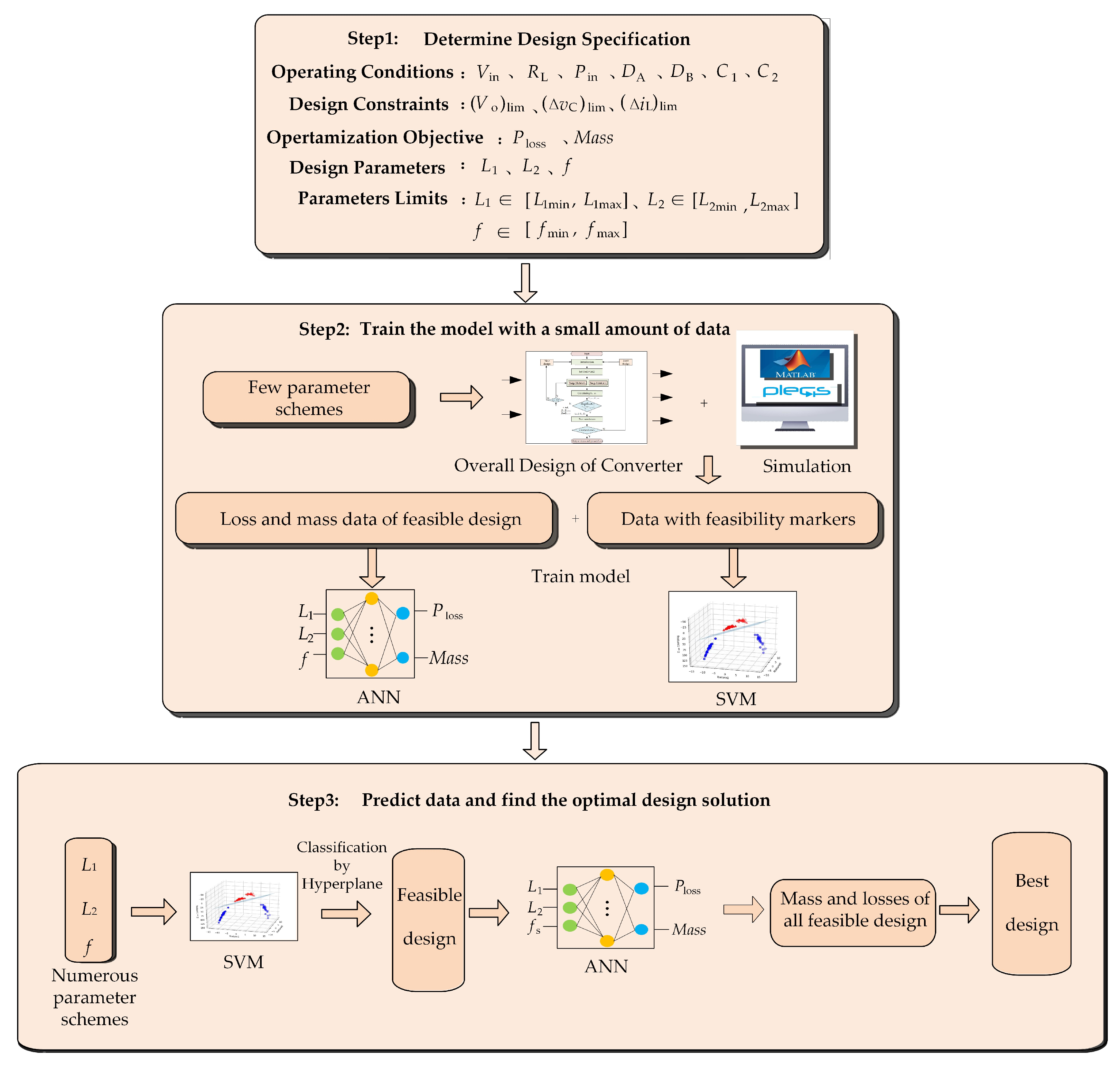
4. Optimal Converter Design Method Based on Machine Learning
On the basis of
Section 3, this study adopts an integrated approach of two machine learning methods to optimize the design of converter circuit parameters. The flow chart of this ML optimization structure implementation scheme is shown in
Figure 6.
The specific steps are as follows:
Step 1: The first step is to determine the design specifications. The design specifications include the operating conditions, optimization objectives, design constraints, design parameters, and parameter limits. This method optimizes
L1,
L2, and switching frequency
f for the mass and loss of the converter. Their optimization limits have different settings at different stages. The constraints and operating conditions of the converter have been mentioned in
Section 3.2.
Step 2: The second step is to train the model with a small amount of data. At this step, this method firstly relies on the overall design flow chart of the converter shown in
Figure 5 and combines circuit simulation to obtain a small amount of data with feasibility marks. These feasible design schemes also contain the corresponding loss and mass data. Then, use these few design schemes and their feasibility markers to train the support vector machine (SVM) classification model. After training the SVM-constrained classification model, these feasible designs, along with their corresponding mass and loss data, are used as training sets for ANN to map circuit parameters to optimization objectives.
Step 3: The third step is to predict data and find the optimal design solution. This step is based on the trained SVM classification model and ANN prediction model to classify and predict numerous circuit parameter design schemes and then find the optimal circuit parameter design scheme from the predicted results. Firstly, the SVM classification model is used to screen feasible design schemes, and then ANN is used to predict the loss and mass of feasible design schemes. Finally, find the optimal design based on comprehensive index ri.
The main motivation for using ML is that, after training ML models with a small dataset, the final optimal design can be quickly found using the exhausted algorithm rather than running the time-consuming simulations over and over again. More details about the use of SVM and ANN will be given below.
4.1. Support Vector Machine for Classification
In this article, SVM is used to classify circuit parameter schemes. The hyperplane in this classification problem refers to the interface that can divide the data in the data space into two categories according to its characteristics in a broad sense. After visualization, it is a line for data containing two characteristics/inputs and a surface for data containing three. The principle of SVM is finding the maximum hyperplane between two types of data, which is in the middle of the interval between two types of data. This optimal hyperplane is unique.
During the training step, the range of inductance
L1 values is set as [20 μH, 420 μH], with a total of 21 discrete values taken at intervals of 20 μH. The value range of inductance
L2 is [50 μH, 1050 μH], with a total of 21 discrete values taken at intervals of 50 μH. The value range of switching frequency
f is [25,000 Hz, 100,000 Hz], with a total of 11 discrete values taken at an interval of 7500 Hz. This generates a total of 4851 points of circuit parameter design schemes to be verified. For the three-dimensional feature space in this article, the original data of SVM is filtered according to the model in
Section 3, where feasible designs are marked as 1 and infeasible designs are marked as 0. Among these 4851 points of circuit parameter schemes, 1816 schemes are feasible, and 3035 schemes are not.
Using these 4851 data points with feasibility markers for SVM model training, in order to improve the accuracy of the SVM model, the raw data are normalized and then input into the model for training. The SVM model is implemented using the ‘fitcsvm’ function in MATLAB 2021b, and its related settings are shown in
Table 5. Calculate the validation loss of the SVM model based on ‘kfoldloss’ to reflect the performance of the SVM model. The smaller its value, the more accurate the model is.
Use 3500 random data points from the original 4851 as the training set and the remaining data as the test set. The training time of the SVM model is 1.84 s, the computational cross-validation takes 14.34 s, and the computational validation loss takes 0.06898 s. The training results show that the validation loss of the model is 0.7%, indicating that the model has good classification performance. Comparing the training results with the actual results, the accuracy of model classification reaches 98%. The training result of the SVM model is shown in
Figure 7.
In
Figure 7, the yellow points are feasible design points, the blue points are infeasible design points, the points surrounded by black circles are support vectors, and the purple surface is the hyperplane of the SVM model.
Generate more parameter schemes in the design space, with 51 values of inductance
L1 taken at intervals of 8 μH in the range of [20 μH, 420 μH]. Inductance
L2 should be uniformly taken as 51 values with intervals of 20 μH in the range of [50 μH, 1050 μH]. In the same way, there are a total of 76 uniform values for switching frequency
f within the range of [25,000 Hz, 100,000 Hz] with an interval of 1000 Hz. In this way, a total of 197,676 data points of parameter schemes are generated in the design space. These parameter schemes are input into the SVM model to obtain their feasibility prediction results, which take about 5 min to predict. Among these 197,676 parameter design schemes, there are 88,591 feasible design schemes. The SVM prediction result is shown in
Figure 8.
4.2. Artificial Neural Network for Mapping
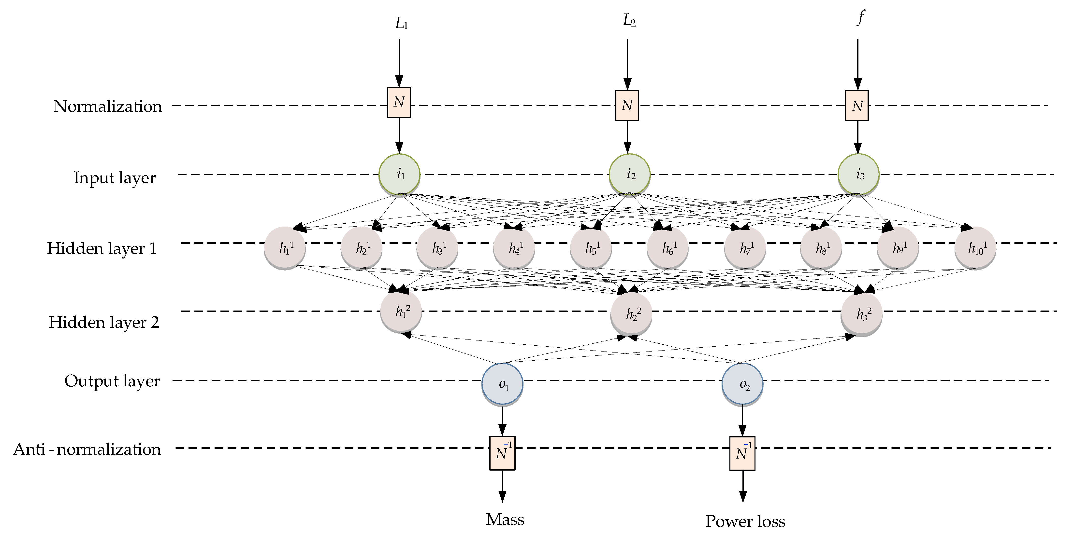
An artificial neural network (ANN) is an algorithm used for information processing. It simulates the way the brain processes information, consisting of a large number of highly interconnected neurons. It solves specific problems by changing the structure, weight, and bias of the network.
Figure 9 shows the ANN structural model used in this article. The input design parameters are normalized and fed into an artificial neural network. Then, after anti-normalization, corresponding mass and loss can be obtained. The established ANN is divided into three parts, including one input layer, one output layer, and two hidden layers. After trial and error in setting ANN hidden layers, it is found that the training performance would be quite good and robust as long as there are two hidden layers and more than three neurons in each layer. Here, the number of neurons in the two hidden layers is 10 and 3, respectively. The ‘
logsig’ function is selected as the transfer function of the hidden layer, the ‘
purelin’ function is selected as the transfer function of the output layer, and the ‘
traingdx’ function is selected as the function of backpropagation.
Use 1816 feasible data points from the training step mentioned in
Section 4.1, along with corresponding mass and loss data, to train the ANN model. The training goal is set to 0.0001, the learning rate to 0.01, and the maximum number of training epochs to 1000. It takes 2.35 s, and the actual training uses 266 iteration cycles. The root mean square error is only 0.0003.
Input 88,591 feasible parameter design schemes obtained from the SVM classification model into the trained ANN model, predict the loss and mass of these schemes, and then select the optimal design scheme based on the comprehensive index
ri from the predicted results. When the comprehensive index
ri reaches the minimum value, the parameter design is considered to achieve the optimal solution. The comprehensive index
ri is defined as follows:
where
Mi is the mass obtained by the i
th solution,
Mmax is the maximum mass,
Plossi is the loss obtained by the i
th solution, and
Plossmax is the maximum loss.
Input the optimized parameter design scheme into the design model of the inductor to obtain the revised design scheme, and then substitute the obtained inductance internal resistance value into the simulation model. Finally, calculate the loss of each part of the converter under the optimized parameter scheme. The design and calculation result are shown in
Table 6.
It can be seen in
Table 6 that compared with the traditional design in
Table 4, although the inductance value of
L1 and
L2 increases, the use of more suitable magnetic cores reduces the total mass.
After optimization, the loss of each part is shown in
Table 7. Compared with
Table 3, the loss of each switch tube and inductance are reduced.
The pie chart of converter loss distribution with the ML method is shown in
Figure 10. Compared with the pie chart of the traditional method shown in
Figure 3, the parameter scheme obtained by the optimization design method reduces the total loss of the converter by about 1.44 W, with a switching loss reduction of about 1.31 W.
5. Experimental Result
According to the results obtained in
Section 2.2 and
Section 4.2, the converter parameters design results based on the traditional method and ML method are shown in
Table 8.
Through simulation analysis, the loss of the optimized converter was reduced from 4.21 W to 2.81 W, and the total mass of the inductor was reduced from 0.19 kg to 0.12 kg. In order to verify the proposed optimization design method, an experimental prototype was built. The rated output voltage is 24 V. The picture of the prototype is shown in
Figure 11.
The prototype includes a main circuit module, a driver circuit module, and a control circuit module.The main circuit module corresponds to the circuit in
Figure 1, achieving power conversion. The driver module used a Si271 isolated gate driver chip and Mornsun’s module power supply to provide sufficient driving energy for the MOSFET. The control module used the DSP28335 chip as the control chip to output the required PWM signal.
It can be seen that capacitors C1 and C2 are composed of patch capacitors in parallel. The switches were selected as IRF3205ZPBF model N-channel MOSFET, with a drain source rated voltage of 55 V, a drain current of 75 A, and a conduction resistance of 7.5 mΩ.
Design the inductance according to the data in
Table 4 and
Table 6. The physical photos of the inductors are shown in
Figure 12; the total mass of the inductors with the ML method is 0.29 kg, which is less than the mass of the inductor with the traditional method of 0.45 kg. Although there is some error between the ML method’s predicted results and the actual values, the mass was reduced by 35.6%.
The converter is designed based on the indicators shown in
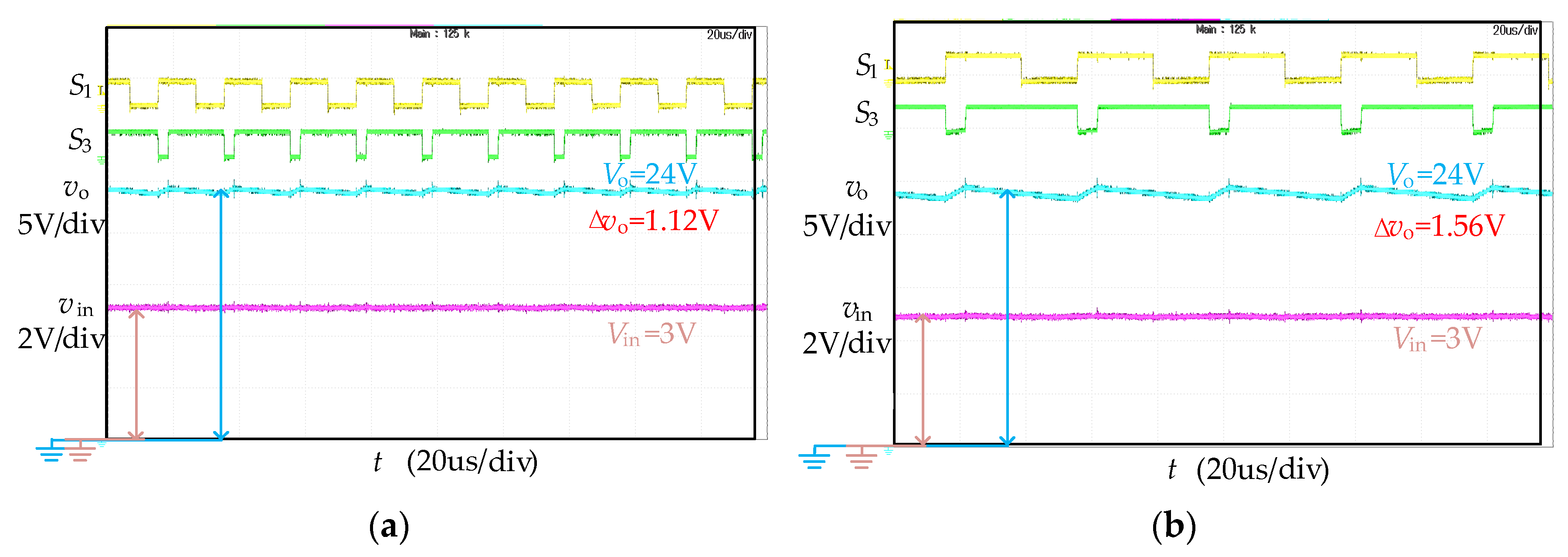
Table 9. Different from simulation, by changing the load resistance to ensure the same boost ratio, we can compare the mass and power loss of the two schemes via experiments. The voltage waveforms and switching drive waveforms with the two methods are shown in
Figure 13. The yellow waveform represents the driving signal of
S1, the green waveform represents the driving signal of
S3, the blue waveform represents the output voltage
vo, and the pink waveform represents the input voltage
vin.The input voltage
Vin and output voltage
Vo of the converter with the two methods are the same. Due to the reduced switching frequency, the voltage ripple of the converter with ML increases from 1.12 V to 1.56 V, but the voltage ripple ratio
ρo still meets the constraints mentioned in
Section 3.2.
The current waveforms and the ripple of the converter with two methods are shown in
Figure 14. The yellow waveform represents the driving signal of
S3, the green waveform represents the input current
iin, the blue waveform represents
i1, and the pink waveform represents
i2.Similar to the conclusion of the voltage waveform, the current ripple of the converter with the ML method increases, but the current ripple ratio
ρL1,
ρL2 still meets the constraints mentioned in
Section 3.2.
The experimental results show that under the same input voltage and power, the converter can operate stably and maintain a constant boost ratio under the set optimization parameters. Due to the decrease in switching frequency, the voltage and current ripple of the converter with the ML method increase but still remain within the constraint range mentioned in
Section 3.2. After calculation, the loss of the converter with the traditional method is 6.55 W, while the ML method is 4.39 W. The loss of the converter was reduced by 32.9%.
6. Conclusions
In this article, a machine learning-based integrated optimization method for SLIC-QBC is proposed to minimize the mass and power loss. This method can automatically use Magnetics’ data to design the inductance model and select the design scheme with the best mass and power loss from all feasible design methods. It has two outstanding advantages: (1) High design accuracy due to the used components’ data; (2) This method avoids the repetitive running process of traditional complex algorithms and saves a lot of time in running simulations.
In the proposed method, based on a component-based inductance design model, SVM and ANN are used to map design parameters to the mass and power loss of the converter. The optimal design scheme is selected using the value of the comprehensive index r. The simulation and experimental results show that the proposed optimized design method can reduce the mass of the converter by 35.6% and power loss by 32.9% compared with the traditional design method in the range of voltage and current ripple.
The main implications of this study are as follows:
(1) Research on the design and optimization of high-gain DC-DC converters for the recycling and utilization of waste batteries.
(2) Proposal of a machine learning-based integrated optimization method to automatically design passive components and switching frequency.
(3) The scheme designed by this method has been verified through simulation and experiments to achieve the optimal combination of converter mass and power loss.
Although this method achieves optimal design for mass and power loss by optimizing inductance and switching frequency, this method relies on a large amount of data to train the neural network, and the lack of data may not achieve the desired training effect. Also, this optimization is achieved within a certain limited design space. If it exceeds this design space, new data need to be collected again. In future research, as this method only targets the passive components of the converter and has no limitation to the topology structure of the converter, we will consider using this method in the topology of other converters to achieve optimal design. Also, more accurate inductance design models can be further established to cover more alternative inductance cores. On this basis, we will research circuit parameter optimization methods with wider applicability.


