Review

Thermoelectric Materials and Applications: A Review

Department of Mechanical Engineering, Politecnico di Milano, 20156 Milano, Italy
*
Author to whom correspondence should be addressed.
Energies 2023, 16(17), 6409; https://doi.org/10.3390/en16176409
Submission received: 14 June 2023 / Revised: 11 July 2023 / Accepted: 22 July 2023 / Published: 4 September 2023
(This article belongs to the Topic Thermoelectric Energy Harvesting)

Abstract

:
Solid-state energy conversion has been established as one of the most promising solutions to address the issues related to conventional energy generation. Thermoelectric materials allow direct energy conversion without moving parts and being deprived of greenhouse gases emission, employing lightweight and quiet devices. Current applications, main thermoelectric material classes, and manufacturing methods are the topics of this work; the discussion revolves around the crucial need for highly performing materials in the mid-temperature range, and around the development of more scalable fabrication technologies. The different manufacturing methods for thermoelectric bulk materials and films are also discussed. Small-scale technologies are generating increasing interest in research; the high potential of aerosol jet printing is highlighted, stressing the many advantages of this technology. A promising approach to scale the production of miniaturized thermoelectric devices that combines high energy ball milling and aerosol jet printing is proposed in the conclusion.

1. Introduction

The worldwide energy and pollution crisis is forcing the industry to innovate in sustainable directions: new ways to harvest and save energy are necessary [1,2,3]. Thermoelectric generators (TEGs) and coolers (TECs) are technological solutions which can address such issues. The operating principle of thermoelectric materials (TEMs) is based on the Seebeck effect, discovered as a thermomagnetic effect by Seebeck in 1821, and correctly addressed as a thermoelectric effect by Oersted in 1825 [4,5]. A thermoelectric (TE) generator is used to convert thermal energy into electrical energy. When a temperature gradient (ΔT) is applied to the opposite ends of a TE device, power is generated according to this temperature difference: the power generated therefore increases linearly with ΔT [6,7,8]. Oppositely, a thermoelectric cooler can generate a temperature gradient between two opposite ends when a current passes through the material from the appropriate pins of the thermoelements. In the first case, converted heat is referred to as the Seebeck effect. In the second case, the phenomenon is called the Peltier effect [1,2,9].
For an ideal thermoelectric generator (e.g., constant TE properties), the maximum heat-to-power conversion efficiency (ηmax) and output power density (ωmax) can be expressed as η max = T H T C T H · 1 + ZT ¯ 1 1 + ZT ¯ + T C T H ; where TC (K) and TH (K) are the cold-side and hot-side temperatures, respectively. The term ZT ¯ (arb. units) indicates the TEG figure of merit (ZT) average value. ZT is defined as ZT = S 2 ρ k T = S 2 σ k T ; here, S (µV⸱K1) indicates the Seebeck coefficient, ρ (Ω⸱m) the electrical resistivity, σ (S⸱m1) indicates the electrical conductivity, k (W⸱m1K1) the thermal conductance and T (K) the applied temperature.
The numerator in the previous equation is known as power factor (PF, Wm1K2) [10]. Therefore, PF is calculated as PF = S 2 · σ . Bell, according to other fellow researchers, concluded that the minimum ZT value to enable the applications of such materials in energy harvesting is equal to 1.5 [11,12,13]. However, despite the non-existing ZT upper limit, applicable TEGs have demonstrated a figure of merit value lower than 1 [14,15].
The disruptive impact of solid-state thermoelectric generators on the world is related to the possibility of directly converting waste heat into electrical energy; currently, research is therefore focusing on these materials thanks to the coupling of sustainable energy production and waste energy re-utilization. The lack of moving parts makes the devices relatively scalable, greenhouse gas emission-free, lightweight, and quiet; furthermore, thanks to these characteristics, thermoelectric devices are extremely reliable. Since these electricity generators do not depend on the nature of the consumable heat, the fields of application are quite numerous and diverse. The five main categories in which thermoelectric generators are used are: medical and wearable devices (e.g., wristband energy harvesters), microelectronics (e.g., wireless sensor networks nodes), electronics (e.g., reutilization of waste heat for energy harvesting), automotive (e.g., re-utilization of engine waste heat to power up devices installed on the vehicle), and aerospace (e.g., energy generation in extreme conditions, such as outer space) [16,17,18,19,20]. TEGs fit these applications because of their reliability, which is the main concern in such cases, not efficiency. Furthermore, in high tech applications such as aerospace and microelectronics, costs are of secondary concern, enabling even more TE material utilization [21,22,23,24]. The last 3 years of state-of-the-art, best performing TE materials (ZT) are summarized in Figure 1. Among the materials cited, those showing the best performance (ZT ≥ 2.4) are GeTe, PbTe, SbSe, and Cu2Se; however, these values did not exhibit high reproducibility, remaining laboratory results never applied in in situ applications. The ZTmax values of similar materials of the years before 2021 are charted in the diagram in the work of Shin et al. [24].
Recent studies about the market of TEMs revealed that in 2019, bismuth telluride accounted for the 66% of the total thermoelectric market. This material is chosen by most companies because today’s commercial applications are close to room temperature, where the highest figure of merit is claimed by Bi2Te3 and its alloys (it can function up to 600 K). Interestingly, the second material in this classification is lead telluride (PbTe) which is used at higher temperatures than bismuth telluride (up to 900 K). Furthermore, PbTe is a chalcogenide as well, indicating the potential of this material class.
Said studies also highlighted that the thermoelectric market is predicted to increase from the 51.9 million USD of 2019 to the 96.2 million USD of 2027, with a compound annual growth rate (CAGR) of 8.0% [25]. This demand derives from the increasing applications in industrial, automotive, healthcare, microelectronics, and aerospace. The advantages of using these materials are related to energy saving (e.g., in many applications conventional batteries could be substituted by these devices, for instance thermo-powered security systems in apartments), the reuse of waste heat (e.g., the heat dispersed by a vehicle engine can be used to power up different accessories of the car), and reducing greenhouse gases emissions, non-renewable sources, and fossil fuel utilization [21,22,24].
Up to 2027, different growth rates have been forecast for the application fields of TEMs (industrial, automotive, electric and electronics, healthcare, and others). Automotive and electric and electronics are the fields where the market is growing the fastest; the value of CAGR is around 9.7% for both, differently from the other fields where it is lower [25].
However, as can be seen from the prices summed up in Figure 1, the high production costs of these devices could lower TEMs’ market growth. An example is in photovoltaic energy generation; a 1000 W photovoltaic panel currently costs less than 3000 USD, whereas a 125 W TEG (where the energy source is sun irradiation) costs 1200 USD. The use of TEMs for such an application has wide potential because when there is no sunlight, an in-house heat source can be used to re-charge the generator. However, the high production prices are not enabling this solution yet [26]. For example, relatively high efficiency values were reached using an n-type (Bi-Te-Se, PbTe) and a p-type (Bi-Te-Sb) for the TEG; however, as summed up in Figure 1, the ZTmax/cost effectiveness is low (0.9 for Bi-Te-Sb and Bi-Te-Se alloys and 1.2 for PbTe), slowing the unveiling on the market [24,26,27,28]. The main research goal is in fact to achieve relatively high efficiency values with scalable processes, delivering TE devices to markets where price is a main concern [25,26,29].
The achievement of high ZT values is related to high values of electrical conductivity and low values of thermal conductivity [15,30,31,32].
The proposed solution to address these issues is to reduce the dimensions and features of TE devices to the nanoscale. This way of boosting ZT was proposed in the 1990s by Hicks and Dresselhaus [33,34], and then supported by other works [29,35,36]. As an example, papers on Bi2Te3/Sb2Te3 superlattices demonstrated a ZT value as high as 2.4, lighting up a spot over this approach. However, these values do not transfer in high performances, because of the high production prices and the low industrial yield [1,9,20].

2. Commercial Thermoelectric Modules

2.1. Characteristics and Manufacturing

TE modules are devices used to exploit thermoelectric phenomena for refrigeration or power generation. These objects consist of semiconductor couples electrically in series and thermally in parallel while being positioned between two ceramic substrates (usually made of alumina, Al2O3, silica, SiO2, or beryllium oxide, BeO); the thermocouples are connected through metal contacts (commercially available products employ thick films of copper Cu between the leg ends and the substrate, which are called ‘interconnects’). Furthermore, an anti-diffusion layer (often nickel, Ni, in one layer or silver, Ag, and tin, Sn, in two stacked layers) is soldered on every element to avoid the phenomenon when the module operates at high temperatures [21,22,37]. More specifically, thermoelectric couples are installed as alternating n- and p-doped semiconducting legs, where the electrons in the n-type legs move like the holes in the p-type legs with heat [13,15]. Doping a semiconductor corresponds to introducing impurities in the material to add an extra electron or a hole. In the conventional case of silicon, p-doping means introducing in the semiconductor 3-valent dopants (e.g., boron) which can catch an outer electron, generating a hole in the material. Oppositely, n-doping means inserting in the semiconductor 5-valent dopants (e.g., phosphorus) which can lose an outer electron, donating an extra electron to the material. Therefore, a p-dopant is an electron acceptor, and an n-dopant is an electron donor [32,38,39].
A single and generic thermoelectric couple is represented in Figure 2.
TE modules can be categorized depending on the configuration: planar, vertical, or mixed. The nomenclature ‘planar’ and ‘vertical’ refer to the direction towards which heat moves relative to the module basal plane.
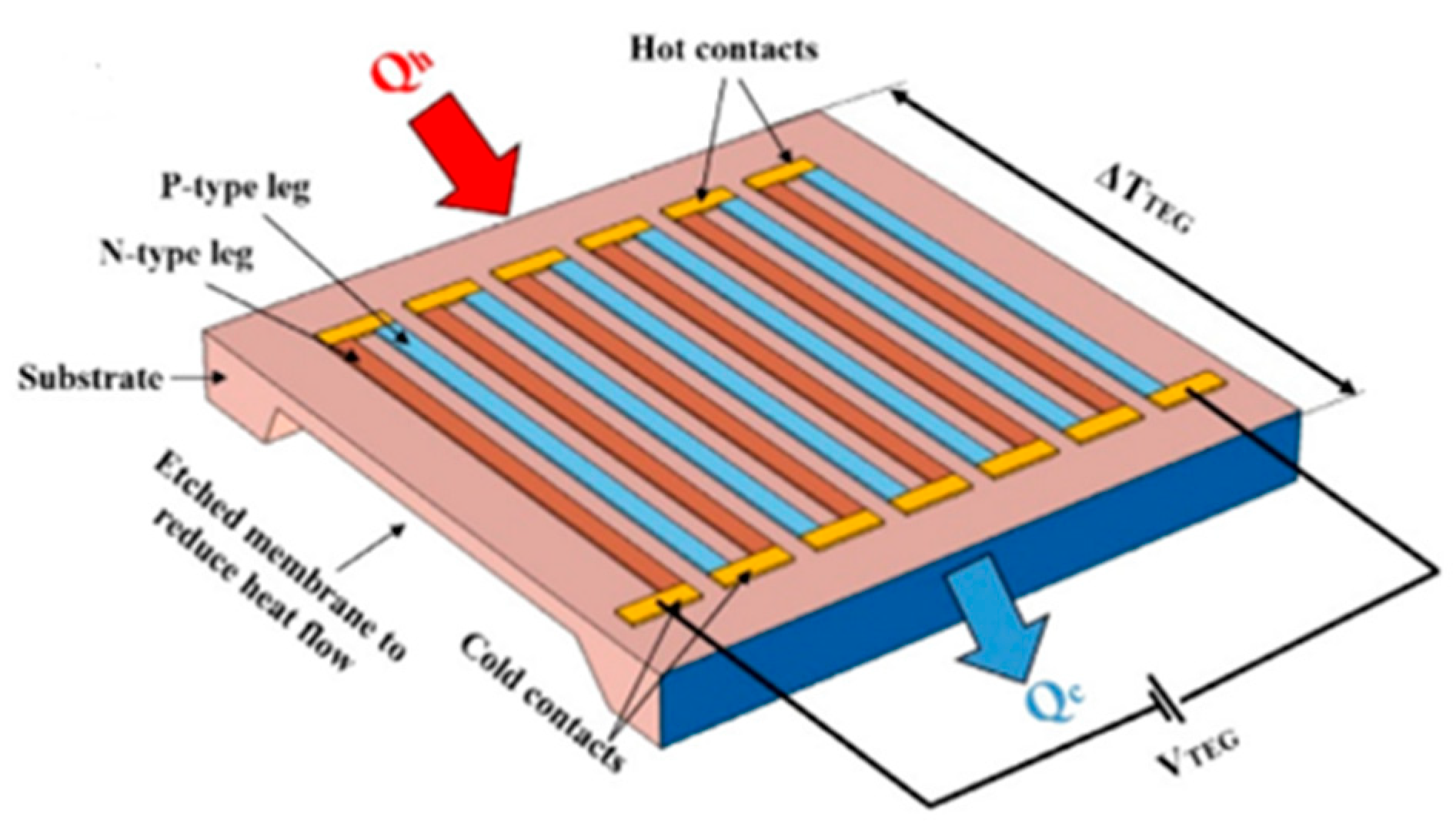
  • Planar design: thermoelectric legs are deposited in such a way that all the cold ends are located on one side of the substrate, and the hot ends on the other one; therefore, the temperature gradient for thermoelectric generation (ΔTTEG) is applied along the substrate surface. This configuration never reached real commercialization because it does not fit most commercial applications. A generic thermoelectric module in planar configuration is shown in Figure 3.
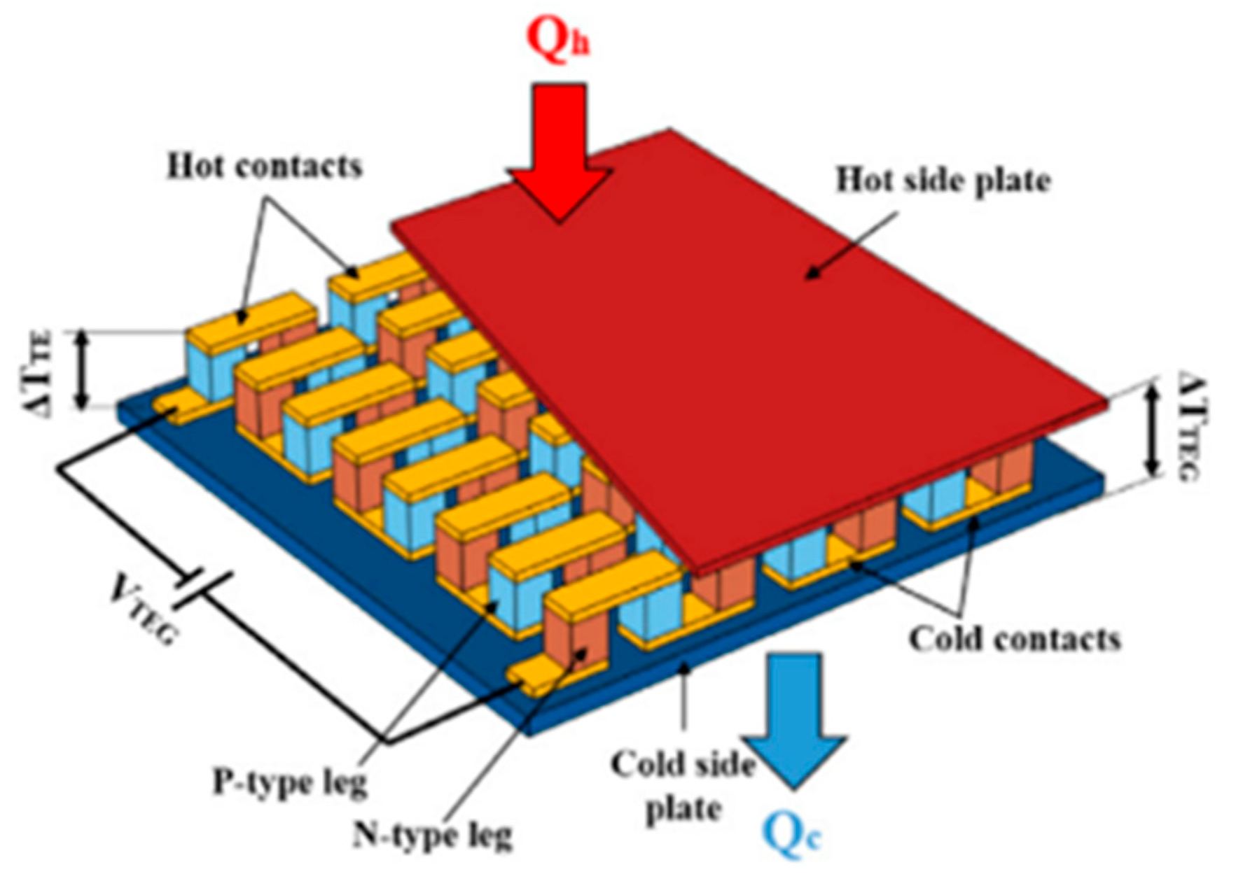
  • Vertical design: in this configuration, the cold ends are located at the opposite sides of the substrate, while the hot ends are in intermediate positions; the deposited thermoelectric legs are shorter and larger in number. In this case, ΔTTEG is perpendicular to the ceramic substrate. This configuration is the most commercialized one and may be found in many appliances. A generic thermoelectric module in vertical configuration is shown in Figure 4.
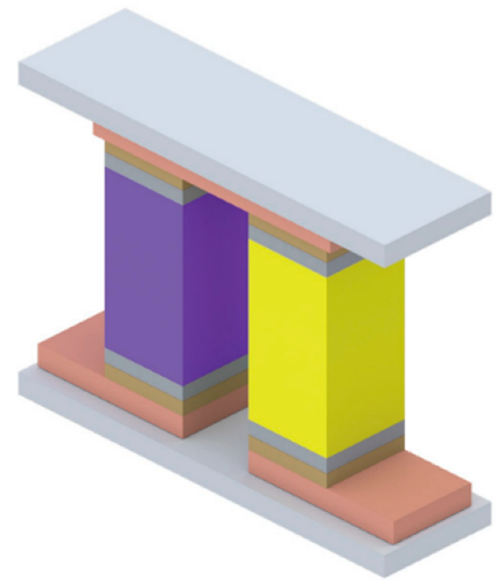
  • Mixed design: this configuration is considered “mixed” because ΔTTEG is located perpendicularly to the module basal plane (vertical design) but the temperature gradient for thermoelectric refrigeration (ΔTTE) is vertical (planar design). Today, this configuration is commercialized for TE refrigeration; however, thanks to its good applicability, it is currently being studied for other applications. A generic mixed configurated TE module is represented in Figure 5 [22,23,37].
A Peltier module SP1848-27145 by Oumefar 40 mm × 40 mm is shown in Figure 6; the device is in mixed configuration and can generate or exploit up to 423 K (150 °C) temperature difference.
No standard for thermoelectric generators dimensions exists; however, it is possible to divide these devices in two categories depending on sizes:
  • Large (or bulk) TEGs: these devices have millimetric sizes and can provide power up to hundreds of Watts when subjected to large heat ranges. TE modules in this category are used for industrial applications.
  • Micro-TEGs: the sizes of these devices are in the range of hundreds of micrometers. These devices work with low waste heat and generate electrical power up to a few mW [15,22,37,40].
The choice between large or micro-TEGs depends on their utilization; a general picture of current applications of commercial thermoelectric generators is presented in Section 2.3.
Furthermore, thermoelectric modules can be classified depending on the substrate chemical composition:
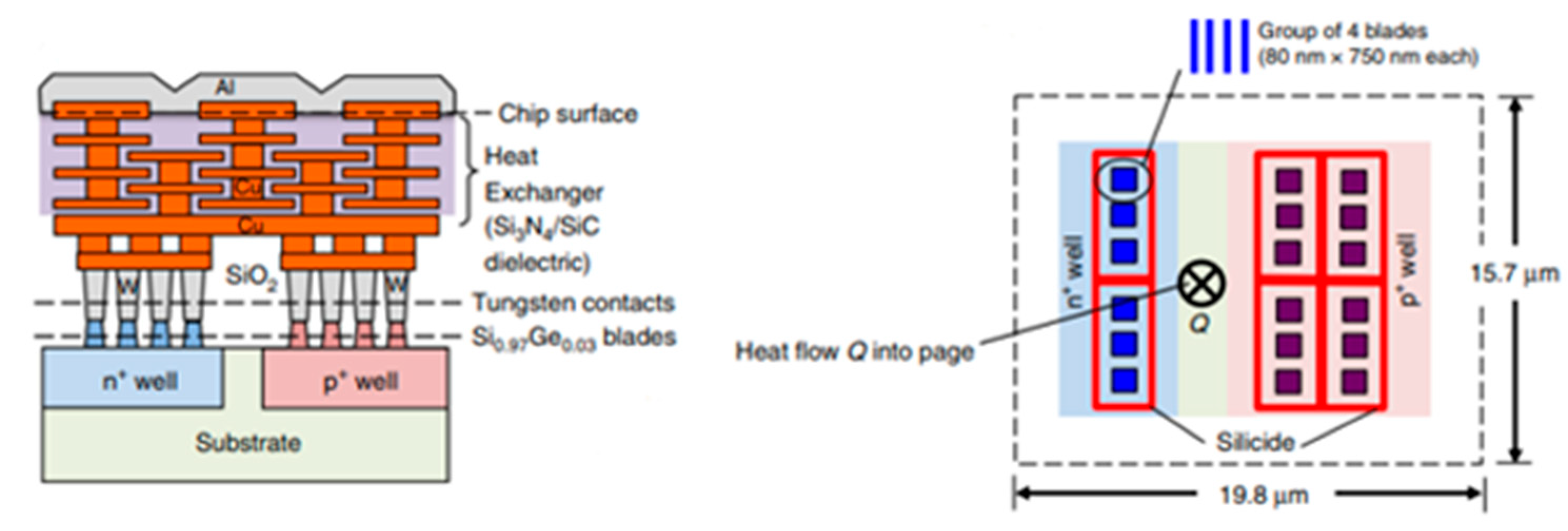
  • Silicon technology (SiO2-based substrates): these substrates are used to fabricate micro-TEGs. The most commonly used materials in these substrates are Si-Ge and Bi-Sb-Te alloys. Given the high temperature resistance and the diffusion shield capacity of silicon dioxide (SiO2), these devices are used for electronics, and more specifically integrated circuits (IC) technology [21,41,42]. The TE n- and p-legs in this case are called n+-wells and p+-wells; often the materials are doped with implantation of arsenic (As) and phosphorus (P) ions for the n+-wells and boron (B) ions for the p+-wells [21,43,44].
  • Alumina (Al2O3): this substrate is often used for high density multi-layered bulk TEGs. Due to the low cost, time-effectiveness, simplicity, and good chemical and temperature resistance, it is used in the industry at high temperatures for high electrical current generation. These substrates can also be used for the fabrication of micro-generators but are more practical for bulk generators [21,45,46].
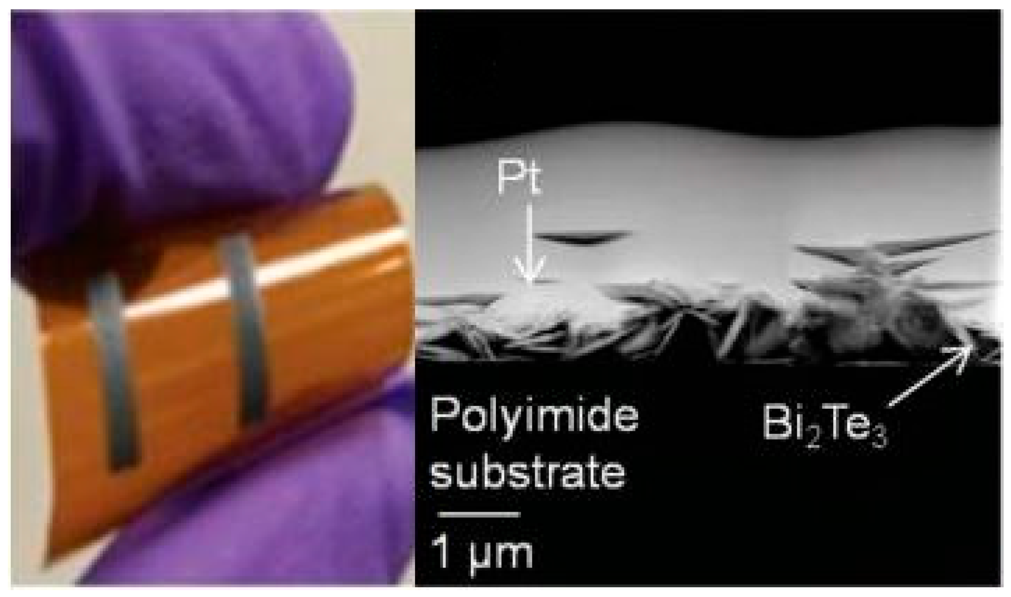
  • Polymers: the most common polymer used for this application is polyimide (PI), cellulose fibers-based materials are also often used. These materials are characterized by a low chemical and thermal resistance while demonstrating high flexibility; micro-generators are fabricated using such substrates for near room temperature applications such as wearable devices or health monitoring applications [21,47,48].
A consolidated industrial manufacturing method has not been defined yet; however, the process can be summarized by an example:
  • Fabrication of the thermoelectric piles (current and promising methods are discussed in Section 4): in industrial plants, it takes place by hot extrusion of thermoelectric materials.
  • The side surfaces of the TE legs are treated to have protection over the environment: a polymeric coating (e.g., water-based paint with fluorine rubber) is deposited by electrodeposition.
  • The TE piles are washed and cured, and then cut to fit a certain module design.
  • Lithography and electrodeposition are used to deposit on the thermopiles surface:
    The metal contacts (usually a single Ni layer)
    The anti-diffusion layer (one Ni layer or two stacked Sn + Ag layers)
    Cu interconnects are often deposited to increase the electrical contact in the circuit (it is a single thick film which does not exceed 5 µm in thickness)
  • The TE modules are assembled by soldering using the applied coating in the form of a tin alloy and gold alloy and using alumina plates as supports [49].
Figure 3. Representation of a TEG in planar configuration. The blue side represents the cold side, the light blue and orange rectangles represent p-type and n-type legs, respectively. Finally, the yellow rectangles represent the metal contacts. Reprinted with permission [21].
Energies 16 06409 g003
Figure 4. Representation of a TEG in vertical configuration. Reprinted with permission [21].
Energies 16 06409 g004
Figure 5. Representation of a TEG in mixed configuration. Reprinted with permission [21].
Energies 16 06409 g005
Figure 6. Oumefar SP1848-27145 Peltier module split in half. Original image.
Energies 16 06409 g006

2.2. Functionally Graded and Segmented Thermoelements

Every thermoelectric material performs better in a certain temperature range; for example, Si-Ge alloys perform better at high temperatures (T > 900 K) and bismuth telluride alloys at lower temperatures (T < 500 K). The most studied approach nowadays is to change microstructural and compositional features of TE materials to achieve higher performances in certain temperature ranges. However, in most applications, the material undergoes wide temperature gradients: regardless of the chosen material, it will not perform as well in one temperature range as it does in another [22,23]. An example is automotive: TEGs composed of segmented thermoelements are applied on the exhaust or radiator of car engines to transform waste heat in electrical current. This choice is due to the large temperature range that occurs close to a vehicle engine during utilization (from 100 to 800 °C) [21,50,51]. The ad-hoc structuring of thermoelectric modules (and therefore the thermoelectric elements composing it) for a certain application has been studied for years to address the above issue [22,23]. Two methods are discussed in current research:
  • Functionally graded TE elements: during the material fabrication, a gradient of dopants is introduced to have a different carrier concentration in the material; specifically, higher towards the hot side to favor the TEG performance. Fabrication of these thermoelements is carried out with the Bridgman technique. This solution proved useful with non-crystal structured TE materials (e.g., bismuth telluride alloys) exploiting the double doping technique.
  • Segmented elements: This solution consists of joining two different thermoelectric materials with different carrier concentration, obtaining the same results as above. This is done with crystal TE materials because grading is not enough to achieve this properties gradient (e.g., skutterudites); currently, these elements are fabricated via sintering of pressed powders [22,23].
Functionally graded and segmented thermoelements are represented in Figure 7.

2.3. Applications of Thermoelectric Modules

Thermoelectric generators can be employed for applications requiring high reliability and where efficiency is not a first requirement, such as micro self-powered wireless devices, health monitoring systems, automotive engines, aerospace, and industrial electronics [9,21,22,23]. As an example, a medical device monitoring the cardiac activity of an individual suffering from heart diseases must be reliable and durable, and efficiency is not a main concern. The categories discussed in this section are medical and wearable devices, wireless sensor networks (WSNs), automotive, aerospace, and electronic and microelectronic devices.

2.3.1. Medical and Wearable Devices

Body heat is a sustainable heat source, and it can be used to supply thermoelectric devices which require small quantities of thermal energy; wearable and medical devices implanted in human bodies fit such requirement [9,21,52]. In several applications such as sports and fitness wearable devices and wireless health monitoring systems, the human body can act as thermal source. The temperature gradient provided to the system mainly depends on two factors: body activities and environmental conditions. However, considering a room temperature of 23 °C and a body temperature of 36 °C, the average temperature gradient is 13 °C, which must be used to provide less than 5 mW (this is for medical devices; sports devices require even less energy).
In the field of implanted medical devices (IMDs), high reliability (fundamental for these applications) and unnecessity of batteries (time consuming and expensive) make TE materials the best choice [9,21,22,53,54,55].
Torfs et al. [53] successfully fabricated a wireless pulse oximeter [56] totally powered by a commercial Bi2Te3-based TEG located on the wrist. The oximeter requires 89 µW to function, and at 22 °C, the TEG generates 100 µW, more than enough to power the system. The watch-like system is represented in Figure 8.
Leonov et al. [57] fabricated a wearable Bi2Te3-based TEG characterized by an output power of 1 µW when subjected to a 13 °C temperature difference. The ceramic plates of the module were made in poly-crystalline Si, normally used for IC technology. This device was applied on a T-shirt, therefore exploiting the heat released by the chest skin of the individual. This application has enormous potential since the person does not have to wear any additional item, but the power is generated from the T-shirt that they would wear anyway during physical activity. The device fabricated by Leonov et al. is shown in Figure 9.
Liu et al. [58] successfully fabricated a wearable TE device for power generation based on n-type Mg3.2Bi1.498Sb0.5Te0.002 and p-type Bi0.4Sb1.6Te3 legs. When the temperature difference was 13 °C (skin-room temperature gradient), the peak output power was 0.206 W·m−2. The TEG also showed good resistance to bending cycles (1000 bending cycles with 13.4 mm bend radius), meaning that it is applicable to flexible substrates. In this case, the power generator was applied on a polymeric matrix (polyurethane) and worn as a wristband. Considering the radius of an adult wrist, the surface can be high enough to enable high energy outputs.

2.3.2. Wireless Sensor Networks (WSNs)

Wireless sensor networks (WSNs) coordinate wireless communication with smart and advanced sensor networks. Today, these systems work with disposable batteries, which release polluting chemicals after their utilization (i.e., Pb, Cr, Cd, etc.); the achievement of battery-free WSNs would be important for green technologies’ implementation in future industry [9,21,59,60]. As the sensor nodes in such devices are miniaturized (microscale), the thermocouples should be very sensitive to temperature gradients and limited in their dimensions. Typically, WSNs in active mode require input power in the range from 10 to 100 µW, and in sleep mode from 10 to 50 µW [9,21,59,61]. WSNs are applied where remote controlled systems are used like heat pipes, water heaters, central heating, and air conditioning systems, thus ranging from building energy management to the industry. Furthermore, these systems are used in the military field, where sensors are used for aircraft security and flight tests, for example [21,61,62].
Lin et al. [61] fabricated a TE-powered WSN for the low-cost environmental sensing in building external structures (building energy management, BEM) through energy harvesting and ultra-low power management. The system was designed in a window frame, exploiting the temperature difference between the interior of the building and the external environment. The experimental part was done using the low-power system on a chip with wireless and Bluetooth functionalities ESP32 by Espressif Systems as a WSN node; it consumes 0.42 mW every 2 h. The system built with a commercial TEG (the material was not clearly identified in the paper; however, since it is a commercial grade material, it was reasonably based on bismuth telluride) generated 1.5 mW under a 6 °C temperature gradient, more than enough for powering the system.
Iezzi et al. [60] manufactured flexible TEGs applicable to commercial steel pipe insulation systems to power the microcontroller for temperature measurements. The fabrication was done by screen-printing commercial low-cost Ag and Ni inks on 125 µm thick polyimide substrate. The device produced an output power of 308 µW when subjected to 127 K temperature difference, which suffices to power up a standard commercial temperature sensing circuit. They demonstrated this point by powering up a standard RFduino system sending temperature readings of the local environment every 30 s to a cell phone via Bluetooth functionalities.
Lineykin et al. [63] developed a thermoelectric energy harvester to replace a 20 Ah disposable battery for a wireless water quality sensor located in a water pipe. They built this device directly on the pipeline surface using commercial bismuth telluride-based TEGs, therefore exploiting the temperature difference between pipeline wall and external environment. The device transmitting the water measurement results via Bluetooth was successfully powered. They demonstrated that with a temperature difference up to 2 K, the device was generating up to 2 mW, enough to power the wireless sensor.

2.3.3. Automotive

High costs of fuel and high carbon dioxide (CO2) emissions are forcing the automotive industry to study new solutions to improve engine performance; currently, many companies (e.g., BMW, Honda, etc.) are showing great interest in thermoelectric generators to address such issues [9,21,64]. Modern studies aim to introduce TEGs that can convert heat coming from internal combustion, thus wasted by the engine exhaust, into electrical energy in commercial vehicles. Depending on the car speed and class, the temperature of the source in the engine can vary from 100 to 800 °C, with a thermal power up to 10 kW. Employing this heat would be vital to increase the engine performance and to power up additional devices in the car (navigation system, telematics, etc.), therefore being helpful in atmospheric pollution reduction [21,65,66]. Segmented thermoelectric modules must be used in this application: the wide temperature range experienced by the TEGs does require different properties for the module. N- and p-type Bi2Te3 are best for the low temperature range (<250 °C), whereas p-type (GeTe)85(AgSbTe2)15 alloys and n-type PbTe alloys for the intermediate temperature range (250–500 °C) are the best choice; lastly, for the high temperature range (500–700 °C), skutterudites (p-type CeFe3RuSb12 and n-type CoSb3) [21,23] are used. Two different locations for the TEGs were presented: between the radiator surface and the fins (maximum temperature difference of 80 °C) and on the exhaust heat system (the heat can be higher than in the previous case, so much so that complex-shaped TEGs may be necessary) [21,50,67,68]. When discussing this application, the term ‘energy saving’ is mentioned, which refers to saving in fuel consumption, costs, and CO2 emissions.
Yáñez et al. [69] applied a commercial Bi2Te3-based thermoelectric generator on the exhaust of two different engines to demonstrate the high recovery of energy in spark-ignited (diesel used as fuel) and compression-ignited (gasoline used as fuel) engines in Ford ecoboost and Nissan YD22 car models, respectively. The applied temperature difference was 50 °C; they also applied different modes for the engine (different rounds per minute, rpm; torque, N·m; and different engine power, kW). However, for the gasoline engine (1700 rpm, 60 N·m, and 10.7 kW), the TEG generated an output power of 16.6 W (potential 0.37% energy saving); for the diesel engine (1250 rpm, 80 N·m and 10.5 kW), the TEG generated instead an output power of 41.6 W (potential 0.84% energy saving). The power generated is enough to possibly power more than one electrical device on the car (such as a navigator).
Orr et al. [51] mounted a TEG on the exhaust of a 3.0 L V6 Diesel Engine. The device consisted of eight commercial Bi2Te3-based TE modules distributed on the exhaust system. The TE device generated up to 37.85 W when the engine was running at 4000 rpm, with no torque applied and at 50 °C temperature difference; they calculated that this could result in a potential 1.57% energy saving.

2.3.4. Aerospace

TEGs for aerospace, or radioisotope thermoelectric generators (RTGs), are spread for space crafts, satellites, and space probes. These devices use the heat transferred by radioactive materials undergoing natural decay to generate electricity. Over the years, different isotopes have been used (Cerium-144, Polonium-210, etc.) but the best, and still in use, is Plutonium-238: high melting point, low gamma radiation, and high half-life (almost 90 years) make it the best choice for this application [9,21,70,71]. The devices must be made of TE materials operating at high temperatures; usually, PbSnTe is used as p-legs and (GeTe)85(AgSbTe2)15 (known as TAGS alloys) as n-legs. In the past, SiGe was often used as well. Today, the costs for single RTGs fabrication are enormous (from 100 to 120 million USD) due to high safety protection costs and low disposal of Pu-238 (1968 USD a gram): the improvement of the radioisotope power system is necessary [21,72,73,74].
In 1989, NASA launched the Galileo space craft, which was installed with the first module, known as GPHS-RTG. The thermal source was Pu-238 and the TEG was mounted as 18 SiGe/SiMo modules. The hot side operated at 1308 K and the cold ones at 566 K, the device provided 245 W of electrical power [21,74,75,76].
About 15 years later, new generation RTGs were installed on spacecrafts. The Multi-Mission Radioisotope TEG (MMRTG) powered by Pu-238 was mounted on the space probe Pioneer 10 for outer space exploration. The devices consisted of 16 PbTe/TAGS modules, where the hot legs operated at 510 °C and the cold ones at 121 °C. The system worked for longer than it was designed for, and it was generating power for 110 W [21,73,74,76]. A cutaway of a MMRTG is shown in Figure 10.
Currently, new solutions are being studied. Holgate et al. [77] fabricated a MMRTG alimented with Pu-238 and composed by 768 skutterudite-based thermocouples. The hot sides of the system operated at 625 °C and the cold ones at 200 °C, generating up to 105 W of electrical power; despite being composed of non-conventional materials for this application, their power value is in the range of the other MMRTGs.

2.3.5. Electronic and Micro-Electronic Devices

When studying microelectronic devices, products such as miniaturized circuits, integrated circuits, and central processing units (CPU) are discussed. Today, processors can produce thermal power in the range from 6 to 320 W and waste heat up to 110 °C. In general, this heat must be removed or used to cool down the device via thermal management technologies to ensure a longer battery life and a better battery performance; the lack of cooling in these utilities can lead this technology to prematurely end its life and to malfunction [9,21,78,79]. Conventional cooling systems for electronics (rotary fans and cooling pipes) were successful in the past, but with the advent of microelectronics and their fast technological advancement, they have partly lost their utility. This technological breakthrough has limited the number of cooling systems applicable to these technologies since the increase in component density and heat flux generation (decrease in size of electronic devices) [21,44,80,81].
The electronic utilities market of 2011–2012, analyzed in 2013, showed that the fabrication of small-sized laptops in those two years grew by around 10 times [21]. This evidences that there is an urgent need to develop thermal modules that ensure the functionality of small electronic devices in terms of size, heat transport capability, and reliability; the main obstacle now is the inability to achieve power densities which are enough to provide an adequate output power to current microelectronic devices, which have areas in the order of mm [2,21,82].
Furthermore, the compatibility between silicon technology and TEGs has not been developed yet, limiting applications in microelectronics [79,80]. Thermal management technologies are currently divided into four classes:
  • Airside: these are the conventional cooling technologies, including rotary fans and heat sinks. The main application of heat sinks is in laptops and located at the heat transfer interface between the heat source and the rotary fans. More innovative solutions in this group are piezoelectric fans and electrostatic fluid accelerators (EFAs).
  • Heat transporters: these solutions were designed for higher heat flux applications. The most common solutions are heat pipes, vapor chambers, cold plates, and liquid and spray cooling; they are always used with rotary fans for thermal management of laptops and computer servers.
  • Active solid-state heat spreader: Thermoelectric devices are part of this group, along with thermotunneling and thermoionic devices. Currently, used TE devices are thermoelectric coolers (Peltier effect usage); however, these are used for niche applications because of their high price. In this field, TE materials are also studied as TEGs, thus using waste heat as source for electrical energy generation: not only by powering other components of the electronic device but also by supplying current to the cooling fans, being active thanks to the waste heat dispersed by their own system.
  • Passive thermal interface material: these solutions are used for cooling by heat transfer and include greases (the most common one based on a silicon matrix), gels, adhesives, and graphene. These materials have extremely lower thermal resistance than air or commercial materials for such purposes (e.g., silver epoxy) and therefore allow for interface cooling [21,79].
Currently, commercially available thermoelectric devices for microelectronics are integrated thermoelectric micro-coolers (ITM), which are employed to stabilize the temperature of solid-state lasers, to cool infrared detectors, and to enhance the performance of integrated circuits. The dimensions of commercially available thermoelectric coolers vary from about 50 × 50 × 5 mm to a lower limit of around 4 × 4 × 3 mm. These devices are structured as Peltier modules and usually are based on bismuth telluride alloys or silicon carbide (SiC) on SiO2 substrates [15,22,23,81].
As a valid example, Huang et al. [81] developed a poly-silicon-based micro-thermoelectric cooler based on bismuth telluride (n-type Bi2Te3 and p-type Sb2Te3) in mixed and bridged configuration; the device is meant to be applied on ICs, and when a current of 80 mA is applied, the generated temperature gradient was of 5.6 K.
As for TEGs, there is currently little use of microelectronics: they can be applied in niche applications where their cost is of secondary concern; therefore, large-scale scalability has not been achieved yet. The most discussed application of TEGs in microelectronics is in WSNs and in technologies such as laptops, smartphones, and tablets [9,21]; therefore, if we identify ‘microelectronics’ as any field of technology where micro components are needed, then this application range is extremely wide. The most studied technology is thin films, since the miniaturized dimensions of the allocations for eventual micro-TEGs.
As an example, Dhawan et al. [43] fabricated a rigid microelectronic device (area < 1 mm2) in Si0.97 Ge0.03 using standard silicon by processing (the n+-wells were fabricated through arsenic ion, As, and phosphorus ion, P, implantation in Si0.97 Ge0.03. The p+-wells were prepared by implanting boron ion, B, in the material); these micro-TEGs would be appropriate for on-chip or in-package integration with energy autonomous ICs. When the applied temperature difference was equal to 15 K, the device produced an output power of 0.3 µW. The whole module dimensions were 15.7 × 19.8 µm, whereas the single thermoelement was 80 × 750 nm, and every single blade of the four composing the module was 65 nm large. The comparison with commercial microelectronic devices based on bismuth telluride demonstrated that this technology has good potential for future applications. A schematic of the device structure is shown in Figure 11.
Hu et al. [44] fabricated a TEG using nanostructured silicon thermopiles produced on an industrial silicon Complementary Metal–Oxide-Semiconductor (CMOS) process line. Studies about this implementation of TEGs are crucial, because making the TE world closer to the microelectronics world is fundamental. The selected substrate was commercial silicon used on a process line for the fabrication of microelectronic devices. The assembly process and the device dimensions are complementary to the work by Dhawan et al. (Figure 11), and the n+-wells were fabricated through arsenic ion, As, and phosphorus ion, P, implantation in silicon and the p+-wells were produced by implanting boron ion, B, in the material. SiO2 was used for filling the space between the legs for mechanical reinforcement. The device showed an output of 0.2 µW when the temperature difference was equal to 20 °C; this result is comparable to common TEG for microelectronics based on bismuth telluride alloys.
Kuang et al. [83] fabricated (via radio frequency magnetron sputtering) n-type Bi2Te2.7Se0.3 and p-type Bi0.5 Sb1.5Te3 based thin films for TE modules in WSNs sensors for energy harvesting. The thin films were deposited on a polyimide substrate in an annular configuration and were composed of a set of 8 to 16 TE legs; the thickness of both n- and p-type legs was about 1 µm and the total diameter of the module was 6 mm. Furthermore, the thin films underwent annealing for 30 min in a controlled atmosphere at 573 K. The TE modules composed of 12 legs showed the best performance: with a temperature difference of 23 K the output power was equal to 169 nW, a value comparable with literature, considering the small surface area of the samples.
As a last example, Kobayashi et al. [84] prepared n-type Bi2Te3 and p-type Sb2Te3-based thin films TE modules in WSN sensors via radio frequency magnetron sputtering. The thin films were deposited on flexible polyimide substrates and the TE modules were characterized by a tubular configuration and 16 p-n paired thermoelements. The overall TE device length was up to 36 mm and the tube radius equal to 7.5 mm, whereas the thin film thickness was equal to 1.5 µm. Finally, the samples were annealed in a controlled atmosphere at 323 K for 60 min. The tubular TEG generates an output power equal to 306.8 nW when subjected to a 20 K temperature difference, which is better performing than Kuang et al. samples. Literature results on the performance of different TE materials by application are summarized in Table 1.

3. Thermoelectric Materials

Thermoelectric materials can be categorized depending on chemical composition, application, temperature of application, and other approaches. In this review, classification is done depending on the material composition and secondarily depending on the application temperature.
Eight main categories can be identified in state-of-the-art thermoelectric materials: skutterudites (SKUs) [86,87], half-Heusler [8,88], clathrates [89,90], zintls [91,92], oxyselenides [32,93], silicon–germanium alloys (Si-Ge) [94,95], organic and hybrid materials [96,97], and chalcogenides [22,32,98]. Furthermore, these materials can be labeled with one of three different temperature ranges:
  • Low temperature range (up to 600 K): common low temperature applications are wearable and medical devices, where the devices are working near room temperature (Section 2.3.2). Microelectronics applications, such as nodes for WSN devices, may be included in this category due to the low heating of such utilities (Section 2.3.1 and Section 2.3.5).
  • Medium temperature range (from 600 to 1000 K): thermoelectric materials are commonly employed in this range in automotive and in industries, where waste heat can be converted into electrical current directly from the engine in the former case and from plants (e.g., heat pipes) in the latter (Section 2.3.3).
  • High temperature range (from 1000 K): this range of application is mainly involved in aerospace to harvest energy for space missions and exploration of outer space, where photovoltaic energy harvesting fails (Section 2.3.4) [21,22,23,24,32].

3.1. Skutterudites

Skutterudites derive from the aristotype cobalt triantimonide (CoSb3), a semiconductor characterized by high carrier mobility (narrow band gap) and relatively large effective electron mass; maximum ZT value for CoSb3 is not higher than 0.8 at around 900 K [86,87]. The most performing and used skutterudites for TE applications are filled SKUs: their structural-chemical formula is EPyT4×12, where EP is an electropositive element species (i.e., iron Fe, nickel Ni, gallium Ga, indium In, etc.), T a transition metal atom (i.e., cobalt Co, rhodium Rh, etc.), and X is a metalloid (i.e., antimony Sb, tellurium Te, etc.) [21,86,99]. As an example, the structure of the filled SKU LaFe4Sb12 is shown in Figure 12.
The temperature range for SKUs application is from RT up to 900 K and they are now considered for applications such as automotive waste heat recovery, thermopiles for high temperature energy harvesting, and aerospace (an example about SKU-based MMRTGs by Holgate et al. [77,101] has already been presented in Section 2.3.4). SKUs are therefore applicable in the low and medium temperature range [86]
Conventional techniques to densify skutterudites are high pressure sintering (HPS) or high pressure-high temperature sintering (HPHTS) on powders which already underwent high energy ball milling (i.e., mechanical alloying). Often, melt spinning is also used for bulk samples preparation [24,86,102]. As an example, Tomida et al. [103] prepared a La0.8Co4Sb12 sample with a diameter of 200 mm, thickness of 21 mm, and a weight of 5 Kg demonstrating ZT = 1 at 773 K.
The highest ZT value reached in literature is around 1.9 at 823 K, and it was achieved by Rogl et al. [104]. This performance was attained when testing bulk samples of n-type triple-filled skutterudite with composition (Sr0.33Ba0.33Yb0.33)0.35Co4Sb12 fabricated by high energy ball milling and then by hot pressing. The most studied n-type and p-type skutterudites are ytterbium (Yb) partially filled skutterudites and didymium (DD)-based skutterudites, respectively; these two fillers can drastically reduce thermal conductivity of the compound. Regarding thin films, Liang et al. [105] deposited Ti-doped CoSb3 thin films on BK7 glass substrate magnetron sputtering. The films were annealed for 2 h in argon atmosphere at 573 K. The final thin film thickness was around 400 nm, and the figure of merit was 0.86 at 523 K.

3.1.1. n-Type Yb-Partially Filled Skutterudites—Medium Temperature Range

The potential of ytterbium (Yb) partially filled skutterudites was brought to light in early 2000s by Nolas et al. [106] and further studies highlighted their potential. As an example, Salvador et al. [102] prepared n-type ytterbium, barium (Yb,Ba)-filled skutterudites bulk samples through melt spinning coupled with solid spark plasma sintering (MS-SPS), followed by annealing at 973 K; the samples stoichiometries were Yb0.08Ba0.09Co4Sb12.12 and Yb0.13Ba0.1Co4Sb12.
The thermoelectric properties of Yb0.08Ba0.09Co4Sb12.12 were high, demonstrating a figure of merit value equal to 1.1 at 700 K. Oppositely, near room temperature the ZT value was around 0.25, which is low and difficult to implement in today’s industry.

3.1.2. p-Type DD-Based Skutterudites—Medium Temperature Range

Didymium is a natural double filler composed of 4.76% praseodymium (Pr) and 95.24% neodymium (Nd). Pr and Nd have relatively large atomic masses compared to small ionic radii; therefore, thermal conductivity is strongly reduced when the voids are filled by these elements [87,107]. This material has been developed recently and is not yet employed in on-field applications; however, at around 800 K, materials such as Ca0.21DD0.43Fe3CoSb12, Ba0.18DD0.48Fe3CoSb12, and Yb0.16DD0.5Fe3CoSb12 showed a ZT value from 1 to 1.1 [86,99]. The highest ZT value in literature so far (1.2 at 700 K) was obtained by testing DD0.65Fe3CoSb12 bulk samples [108]. Rogl et al. [107] demonstrated that the material DDy(Fe1−xCox)4Sb12 with 0.3 ≥ x ≥ 0.2 and y = 0.60 or 0.65 shows ZT values between 1.1 and 1.2 at 700 K; the authors stated that this didymium-based material is an extremely promising p-type TEM. As a final example, Rogl et al. [109] fabricated first via optimized melting reaction and then by mechanical alloying bulk samples of DD0.54(Fe1−xNix)4Sb12 with 0.25 ≥ x ≥ 0.13. This material (cheaper than DDy(Fe1−xCox)4Sb12 because of Ni employment) shows a figure of merit equal to 1.1 at 700 K when x = 0.15 and y = 0.54, comparable to DDy(Fe1−xCox)4Sb12 performance.

3.2. Half-Heusler Alloys

Heusler alloys are ternary intermetallic compounds characterized by a MgAgAs-type crystal structure; the difference between Heusler alloys and half-Heusler alloys is that the sublattice of the former is totally occupied, whereas that of the latter is partially occupied [88,110,111]. The two structures of the alloys are represented in Figure 13.
Half-Heusler alloys are better thermoelectric materials than full-Heusler ones because they have a small band gap, low electrical resistivity, and high thermopower (i.e., high Seebeck coefficient) [20,110,112]. Recently, Ni and Sn have been substituted to get better performances; Fe and Co replaced Ni, and Sb substituted Sn. Multiple filling was also explored, for example by preparing materials such as Nb0.88Hf0.12FeSb and Ta0.74V0.1Ti0.16FeSb; promising results were achieved with different compositions. As an example, Zhu et al. [113] reached a figure of merit of 1.42 at 973 K when testing the multiple filled p-type material ZrCoBi0.65Sb0.15Sn0.2. These alloys can be applied from room temperature up to 1300 K depending on their composition (the whole temperature range), but the best performances are attained at around 800 K. Currently, there are no commercial applications for these materials because achieving high ZT values is hindered by high contact resistance between the interconnects and the TE leg; promisingly, the free-standing materials can show high performances. At present, the most studied half-Heusler compounds are p-type XVFeSb (XV = vanadium V, niobium Nb, and tantalium Ta) and ZrCoBi, and n-type XIVNiSn (XIV = Ti, Zr, and Hf) and XIVCoSb (XIV = Ti, Zr, and Hf). However, since the promising results in literature, the focus will be on p-type XVFeSb and n-type XIVNiSn [20,24,111,114].

3.2.1. p-Type XVFeSb—High Temperature range

The most impressive characteristic of this material family is large power factor (S2σ) over a wide temperature range; most of these materials keep a power factor value over 5–6 mW⸱m−1⸱K−2 from 300 up to 1200 K. Generally, these materials are prepared first by ball milling or levitation melting and then by sintering the powder to form bulk samples, followed by low temperature annealing (at about 750 °C). As an example, Fu et al. [115] fabricated FeNb0.88Hf0.12Sb bulk samples showing a ZT value equal to 1.5 at 1200 K, and from 300 to 1200 K; the samples were prepared via levitation melting and spark plasma sintering (SPS), concluding the process with a 3-day-long sintering process at 1073 K. Concerning the power factor, at 1200 K, this material showed a PF value of 5.8 mW⸱m−1⸱K−2. To conclude, this material has good performance, but it should be utilized at high temperatures.

3.2.2. n-Type XIVNiSn—Medium Temperature Range

Nowadays, there are no reproducible examples of high TE performance for these half-Heusler in the literature; however, some features of this class of materials are extremely interesting. The XIVNiSn need very low doping to optimize the power factor; p-types require atomic substitution at around 20% to maximize the response, whereas these phases just need around 1 to 2% to attain the same optimization level. They also present some full-Heusler phases, which can be beneficial for the performance. A high figure of merit values was not reached yet; however, the potential of this half-Heusler material family is high. The highest performance to date has been achieved by Kang et al. [116] by introducing tungsten (W) nano-inclusions in the material; they fabricated n-type Hf0.6Zr0.4NiSn0.99Sb0.01 + 5 wt% W powder by radio-frequency induction melting, followed by mixing with tungsten nano-powder and densification by spark plasma sintering. This material showed a figure of merit equal to 1.4 at 773 K, mainly thanks to the introduction of the nano-powder, which functioned both as electron-injector and as filtering effect that enhanced the thermopower of the material.

3.3. Clathrates

In a similar fashion to skutterudites, clathrates are characterized by a cage-like structure that allows thermal conductivity engineering via insertion of atoms in the material structure. This crystal structure is related to type I and type II clathrate hydrates, such as (Cl2)8(H2O)46 and (CO2)24(H2O)136 [89,117,118,119]. The general formula representing type I clathrates is X2Y6E46, where both X and Y are guest atoms (alkali metals, rare earth, or alkaline earth elements which are not strongly bonded to the structure) and E represents an element of the group XIV (Si, Ge, or Sn); the formula for type II clathrates is instead X8Y16E136 [21,24,89,90,120]. The crystal structure of type II clathrate CsNa2Si17 is shpwn in Figure 14. A lot of work has been done around type I structure in recent years, trapping many di fferent atoms inside the polyhedra, such as alkali metals and rare earth atoms. The extremely low thermal conductivity is the most attractive feature of type I clathrates, which in some cases was comparable to the thermal conductivity of amorphous materials. An example is the glass-like thermal conductivity of Sr8Ga16Ge30; the lattice thermal conductivity kl was determined to be around 8 W⸱m−1⸱K−1 [89,117,118,121]. The other clathrates families are type VII, twisted, VIII, and IX; however, a few compounds reached stability so they are not widely studied for TE applications [90].
The synthesis of clathrates samples is usually carried out with different methods depending on their dimensions. The fabrication of microscopic samples is usually done by thermal decomposition or solid-state synthesis; the macro samples are produced with well-established routes such as the Czochralski method [89,122] or vertical Bridgman growth [89,123]. Currently, TE applications based on clathrates have not been developed yet, but the studies highlighted that the best performance is achieved in the medium and high temperature range [89,90,121]. The most studied materials, which also yielded the best TE performances, are usually based on gallium and germanium [55,118].
These materials show high TE performance in the medium/high temperature range, but reaching their peak in the high T range. As an example, Saramat et al. [124] prepared 46 mm long crystals of n-type Ba8Ga16Ge30 using the Czochralski method, the TE properties were assessed on disks cut from these samples; the crystals are shown in Figure 15. The figure of merit value was 1.35 in the medium temperature range (900 K) and 1.63 in the high temperature range (1100 K). This performance is interesting and shows potential for future applications in both ranges.
Furthermore, Toberer et al. [119] prepared p-type Ba8Ga16Ge30 samples through grinding then hot pressing followed by vacuum annealing for 60 min at 827 °C. It resulted that in the low temperature range, the TE performance is not high: the highest reached figure of merit was around 0.5 at 773 K.

3.4. Zintls

Zintls are ternary compounds structured like CaAl2Si2; their formula is AB2C, where A = magnesium Mg, calcium Ca, strontium Sr, barium Ba, europium Eu, or ytterbium Yb, B = magnesium Mg, zinc Zn, or cadmium Cd, and C = phosphorus P, arsenic As, antimony Sb, or bismuth Bi [91,125,126]. The crystal structure of zintls is represented in Figure 16.
These materials were studied as p-type thermoelectric materials, demonstrating a high potential in this field. The strong lattice anharmonicity is intrinsically the cause of low lattice thermal conductivity and tunable valence-band structure enables high electrical performance [91,127,128,129].
Materials such as Yb14MnSb11 [126], Yb9Mn4.2Sb9 [125], and Ca5Al2Sb6 [130] demonstrated the highest TE performances thanks to their intrinsically low lattice thermal conductivity. These materials show an intrinsic p-type behavior and can operate in any temperature range depending on composition [91,92]. Currently, the focus is mostly on polycrystalline samples fabricated either by high-energy ball milling followed by high temperature sintering (hot pressing or spark plasma sintering), or by melting and subsequent annealing, followed by consolidating processes. Zintls currently yielding the highest TE performance are the ones where B = Zn and C = Sb [92,126,130].
These materials yield the highest performance thanks to the extremely low thermal conductivity, which can also be achieved via band engineering (e.g., band alignment). Aside from Zn and Sb, the other components of the high performance zintls are often cadmium Cd and ytterbium Yb [24,91,127].
The highest ZT peak in a zintl was in fact reached in 2018 by Wang et al. [92] testing bulk samples of Yb1-yBayCd2-xZnxSb2 (with y = 0, x ≤ 0.9; x = 0.5, y ≤ 0.1). Those samples were prepared by hot-pressing a powder obtained by hand-grinding ingots fabricated in vacuum quartz ampoules at 1273 K for 2 h from pure powders with stoichiometric composition. They achieved a figure of merit value equal to 1.3 at 700 K when the zintl composition was Yb0.96Ba0.04Cd1.5Zn0.5Sb2, also employing band alignment. As a final example, Zheng et al. [131] achieved a figure of merit value close to 0.9 at 700 K by testing EuCd1.4Zn0.6Sb2. The samples were polycrystalline and bulky; in a similar fashion to Wang et al., they prepared the samples themselves by forming the ingot, which was then ground to obtain a fine powder which was hot-pressed at 823 K for 50 min with uniaxial pressure of 80 MPa.

3.5. Oxyselenides

Oxyselenides are oxy-chalcogenide compounds containing selenium of general formula RMCSeO (R = bismuth Bi, cerium Ce, or dysprosium Dy, M = copper Cu or silver Ag, Se = selenium, and O = oxygen). Between the pristine oxyselenides, the highest performance was shown by BiCuSeO, which behaves as a p-type semiconductor, it crystallizes in a layered ZrCuSiAs structure type where Bi2O2 layers are alternatively stacked with Cu2Se2 layers, as represented in Figure 17 [35,112,132,133,134].
BiCuSeO has a low electrical conductivity in comparison to state-of-the-art TEMs because of its low carrier concentration; doping is in fact the main strategy to enhance its figure of merit [132,133]. However, what makes oxyselenides attractive materials for TE applications is the intrinsically low lattice thermal conductivity due to the slow transport of phonons resulting from the soft bonding (low stiffness) [112,135]. Pristine BiCuSeO can reach a figure of merit of 0.5 at 900 K thanks to such low thermal conductivity, but the improvement in electrical conductivity (mainly through dopants) has resulted in a maximum value of 1.4 at 923 K [132]. Currently, TE devices based on BiCuSeO are not present on the market, but many papers highlighted that doping this material with magnesium Mg, cadmium Cd, and barium Ba led to higher TE performances, therefore adapting the general formula to Bi1−xMxCuSeO, where M is the dopant, which is located on the copper site [21,24]. BiCuSeO alloys work as p-type semiconductors and perform better in the upper medium/lower high temperature range (between 850 and 925 K) [132,133]. In the following section, a few examples are displayed.
As an example, Li et al. [136] fabricated Bi1−xBaxCuSeO (with x = 0, 0.025, 0.05, 0.075, 0.1, 0.125, and 0.15) bulk samples demonstrating a ZT value of 1.1 at 923 K. The samples heavily doped with barium were prepared by crushing the ingots sintered by hot pressing powders in stoichiometric ratio (573 K for 8 h or 1073 K for 24 h), followed by ball milling of the obtained coarse powder and consolidation by spark plasma sintering. The disk size was diameter 20 mm and thickness 7 mm. The thermal conductivity was equally slow for these materials, but the electrical conductivity after doping was at its higher value when the stoichiometry was Bi0.875Ba0.125CuSeO, which showed ZT value 1.1 at 923 K. As a last example, Farooq et al. [137] fabricated bulk samples (15 × 3 × 3 mm3) via spark plasma sintering of hand-crushed annealed powders (573 K for 8 h and 873 K for 24 h), which were previously prepared via cold-pressing of ball-milled commercial powders in stoichiometric ratio. The doped material had general formula Bi1−xCdxCuSeO (with x = 0.01, 0.05, and 0.1) and in this case, the dopant did not significantly influence thermal conductivity, but it greatly increased the electronic one. The best TE performance was shown by the most doped formulation Bi0.9Cd0.1CuSeO, which at 923 K, demonstrated a ZT value equal to 0.9. These materials still need extensive study but are promising solutions for TE applications.

3.6. Silicon–Germanium (Si1−xGex)—High Temperature Range

Since silicon and germanium are completely miscible, silicon–germanium (Si-Ge) alloys are under consideration as solid-solution semiconductors, whose formula is Si1-xGex; furthermore, it has a diamond-like lattice structure (Fd3m, Figure 18) characterized by a hexagonal cell [22,32,95].
Si-Ge alloys yield better TE performance in the high temperature range (especially from 1100 K to 1400 K) [95]; nowadays p- and n-type doped Si80Ge20 alloys have been applied in aerospace [74,138] and automotive [21,69]. An attractive aspect of Si-Ge alloys is the relative ease in preparing n-type and p-type semiconductors; the former can be achieved via microstructural control (grain boundaries, dislocations, etc.) and alloying (often by adding phosphorous, P, on the germanium site); the latter can be achieved by dopants on the silicon site (a high performing dopant is yttrium silicide, YSi2, and a common one is boron, B) [95]. Recently, the TE performance was enhanced using nano-inclusions [139,140]. An example of n-type high performance Si1−xGex material with nano-inclusions and an example of a p-type high performance Si1−xGex without nano-inclusions are displayed here. The first case is extracted from the work by Mackey et al. [141]; they fabricated a silicon–germanium matrix with precipitated tungsten disilicide nano-inclusions (p-type boron (B)-doped Si/Ge-WSi2 and n-type phosphorous (P)-doped Si/Ge-WSi2) bulk samples. In the first place, they used mechanical alloying starting from the elemental powders to prepare a suitable powder, that was successively consolidated using spark plasma sintering (SPS) from 1073 to 1373 K for 10 min with a 35 kN uniaxial load. They demonstrated that the n-type sample (doped with P) with higher nano-inclusions content (P dopant 2 vol%—Si80Ge20—5 vol%WSi2) performed better than the other samples, showing at 1173 K a ZT value equal to 1.16.
As a final example, Bathula et al. [142] successfully prepared high performing nano-structured bulk samples (disk with diameter around 12.7 mm) of p-type (boron (B)-doped) Si80Ge20. They fabricated the samples similarly to Mackey et al., therefore starting from mechanical alloying of the stoichiometric quantities of elemental powders and finally employing SPS (from 1173 to 1423 K for 3 min with a uniaxial load equal to 60 MPa) to consolidate the prepared powders. The samples (with an unspecified amount of dopant) showed a ZT value equal to 1.2 at 1173 K; both these results highlight the potential of these materials, especially in a temperature range that has few alternative solutions.

3.7. Organic and Hybrid Materials

The most popular organic TEMs are polymers, followed by carbon-based materials. These solutions would be crucial to implement flexible and wearable self-powered devices in today’s industry, currently lacking in the market but extensively studied [21,143]. Furthermore, most organic materials are cheaper, more available on Earth, intrinsically more flexible, and worst thermal conductors than, for example, traditional chalcogenides such as bismuth telluride. Another interesting characteristic of organic materials is the high TE performance around RT in comparison to conventional thermoelectric materials [21,24,135,143]. Finally, this topic is extremely wide and since this review revolves around the more consolidated inorganic TEMs, information is briefly summarized in this section. However, the referenced literature will provide a better insight over this TEM class. The Internet of Things (IoT) is quickly growing within society and fast development of low temperature bismuth telluride-based TE devices led to a higher need for wearable and flexible devices. Recently, implementation of TEMs in polymers and other organic materials has been studied as a possible solution to this problem. However, this is still part of research because high TE efficiency values are still far from being achieved [21,24,143]; highly performing TE polymeric materials can reach ZT values not higher than 0.75 [144]. The main reasons for these low performances are the extremely low electrical conductivity and Seebeck coefficient that characterize these materials. As mentioned, these materials are applicable in the low temperature range, and are currently used as substrates or supports for chalcogenides that perform at low temperatures (e.g., Bi2Te3) [21,24,32]. The most studied organic materials for TE applications are conducting polymers and carbon-based materials.

3.7.1. Conducting Polymers—Low Temperature Range

Conducting polymers are called π-conjugated polymers, their best quality is that of having adjustable levels of doping and a wide variety of usable doping elements [143]. The most common fabrication techniques for these materials are by layer-by-layer assembly [145], in situ polymerization [146], electrospinning [147], and spin coating [148]. The most used conductive polymers are poly(3,4-ethylenedioxythiophene) (PEDOT), poly(3,4-ethylenedioxythiophene) polystyrene sulfonate (PEDOT:PSS), and polyalanine (PANI) [143]. Currently, the TE performances are extremely low. As an example, the top performance was achieved by Fan et al. [144], reaching a ZTmax value of 0.32 at RT testing PEDOT:PSS films which underwent surface ion accumulation. Among the polymeric materials that are applied for thermoelectric means in the low temperature range, PEDOT:PSS are the most studied. PEDOT:PSS solutions are not commercially applied, and the studies about these materials address wearable and self-powered applications. The low temperature range is considered because at higher temperatures, the polymers would degrade and secondarily because the potential applications require very low temperatures. Mengistie et al. [149] prepared both bulky and thin samples of formic acid-doped PEDOT:PSS starting from an aqueous solution of this polymer; the doping was carried out through established consolidated surface treatment. The bulky samples had a thickness of 100 µm and were prepared by vacuum filtration, whereas the thin samples were prepared by spin coating and reached a thickness of 200 nm; both were prepared on glass substrates. After testing the samples, the thin film exhibited the best performance, which corresponded to a ZT value of 0.32 at room temperature.
As a final example, following a well-established procedure, Bubnova et al. [150] deposited a 200 nm thin film of PEDOT:PSS polymerized with iron tosylate as a dopant, on a glass substrate, via spin coating. The final TE figure of merit value around RT was equal to 0.25. These two papers highlight two of the higher TE performances achieved with this class of materials.

3.7.2. Carbon-Based TE Materials—Low Temperature Range

Carbon-based 2D materials are extremely promising in many different fields thanks to their low fabrication cost, high efficiency, and flexibility [151,152,153]. Currently, the most studied carbon-based material for TE devices are carbon nanotubes (CNTs), which can be used both as p- and n-type semiconductors, but largely studied as the former; the p-type conduction is conventionally induced by oxygen doping, and the n-type is induced by introducing functional groups using polymers [21,24,143]. However, the performance is very low; for instance, p-type single wall carbon nanotubes (SWCNTs) doped with O2 reached a top RT figure of merit of 0.027 [154]. Graphene has also been studied as p-type conductor, but integrated in hybrid TEMs, which are better discussed in Section 3.7.3. In a similar fashion to polymeric materials, these solutions can be applied in the low temperature range [143]. Zhou et al. [155] prepared oxygen doped p-type carbon nanotubes films (thickness up to 500 nm) by floating catalyst chemical vapor deposition (FFCCVP) method. They obtained a figure of merit of around 0.021 at RT. Fukumaru et al. [156] fabricated n-type cobaltocene(CoCp2)-encapsulated SWNTs 30 µm thick samples (nominated CoCp2@SWCNTSs) through a previously established encapsulation synthesis process [157]. They demonstrated that at 320 K, the ZT value was equal to 0.157. The sample is shown in Figure 19.

3.7.3. Organic Hybrids Materials—Low Temperature Range

Incorporating organic and inorganic compounds into organic TE materials to fabricate an integrated matrix is an effective way to enhance the TE performance of materials by reducing thermal conductivity [20,158]. The most recurrent studies are about the implementation of conventional TEMs in a carbon-based or polymeric matrix. Depending on the material class, p-type or n-type semiconductors can be fabricated; however, it is generally difficult to achieve very high performance and the potential applications should be in the low temperature range [21,24,143]. Wang et al. [159] employed a complex process (including nanosphere lithography and thermal evaporation) to deposit PEDOT/p-type Bi2Te3 hybrid films on a polystyrene substrate; the films were around 56 nm thick. They tested the film, demonstrating that at room temperature, the material attained a figure of merit equal to 0.57, which already almost doubles the best performance of free-standing carbon-based materials. Li et al. [160] fabricated bulk samples of graphene nanosheets (GNs)/(Bi2Te3)0.2(Sb2Te3)0.8 with different graphene contents (f = 0, 0.1, 0.2, 0.3, and 0.4 vol.%). The preparation consisted of: (a) milling a (Bi2Te3)0.2(Sb2Te3)0.8 ingot fabricated by hot pressing commercial powders, (b) dispersing the powder in a colloidal dispersion of graphene nanosheets in acetone, and (c) stirring until obtaining dried powder. Finally, the GNs/(Bi2Te3)0.2(Sb2Te3)0.8 powders were hot pressed to obtain bulk bars (1.5 × 3 × 10 mm3). The best TE performance was shown by the 0.3 and 0.4 vol.% GNs/(Bi2Te3)0.2(Sb2Te3)0.8 samples, which at 300 K and 440 K showed ZT values of 1.29 and 1.54, respectively. This result is promising for future developments; however, it is not highly replicable.

3.8. Chalcogenides

A chalcogenide is a chemical compound consisting of at least one chalcogen anion (elements of the group 16, such as tellurium Te, sulfur S, and selenium Se) and at least an electropositive element (such as bismuth Bi, lead Pb, and tin Sn). The most used chalcogenides in TE applications are commonly IV–VI compounds (PbTe, SnSe, GeTe, etc.) and V–VI compounds (Bi2Te3, Sb2Te3, Bi2Se3, etc.); these compounds crystallize in the rock-salt structure [21,22,23,24]. The most used materials on the market are called BST (bismuth–antimony or selenium–telluride) compounds and are often used in cooling for electronics and other fields (Section 2.3.1, 2.3.2, and 2.3.5) [22,23,135,161]. Other ternary compounds are also largely studied but not as applied as BST; a promising ternary chalcogenide class is represented by thallium tellurides (i.e., Tl9BiTe6, Tl8.05Sn1.95Te6, etc.) [162]. As an example, Duong et al. [162] prepared a Bi-doped SnSe single crystal with a ZT value of 2.2 around 773 K; currently, this is the highest ZT value in literature for bulk materials. Chalcogenides are the most widely employed materials for thermoelectric applications, almost 75% of the entire thermoelectric market is occupied by bismuth telluride (Bi2Te3) and lead telluride (PbTe) [25]. Among the state-of-the-art thermoelectric materials, these two tellurides have the largest figure of merit near room temperature. Tellurium is so effective because it is heavier and less ionic than the other chalcogens used for such applications; the former characteristic is advantageous for reduced thermal conductivity, the latter for enhanced electrical conductivity [21,24,32]. Chalcogenides can be employed both at low and intermediate temperatures, depending on their composition. Wearable devices, automotive, healthcare system devices, and microelectronics (e.g., miniaturized sensors) are the most common fields of application [6,22,32].
The materials discussed in this section are the most widely studied chalcogenides for TE applications: lead telluride (PbTe), tin telluride (SnTe), germanium telluride (GeTe), and bismuth telluride (Bi2Te3) and their respective alloys.

3.8.1. Lead Telluride (PbTe) and Its Alloys—Medium Temperature Range

Lead telluride (PbTe) has a highly symmetric rock salt crystal structure with the Fm-3m space group, being characterized by face centered cubic (FCC) lattice. This semiconductor can show both p-type behavior (tellurium-rich PbTe) and n-type behavior (lead-rich PbTe) [23,163]. This material particularly shows a good figure of merit in the mid temperature range from 500 to 800 K, being a promising TEG for applications as automotive [22,163,164]. The structure of PbTe is shown in Figure 20.
Girard et al. [165] fabricated bulk samples (2 × 2 × 10 mm3) of sodium (Na)-doped Pb1−xNaxSyTe1−y. The synthesis was carried out by firstly preparing Pb1−xNaxTe and Pb1−xNaxS via hot pressing and crushing, finally melting the two powders together (up to 1383 K) and subsequently rapidly cooling the molten material. The structure of the material consists of a PbTe matrix in which nano-domains of PbS are dispersed and finally the Na-doping was performed to attain a p-type semiconductor. The highest TE performance was achieved by the Pb0.88Na0.12S0.12Te0.88 material, which demonstrated a ZT value equal to 1.8 at 800 K. Although this material is highly expensive, the promising TE properties highlight the potential of this telluride.
A scanning/transmission electron microscopy (S/TEM) image of a Pb0.88Na0.12S0.12Te0.88 sample is shown in Figure 21.
As a final example, Wu et al. [166] prepared sintered bulk samples of NaxEuySnqPbx+y−qTe. They first prepared the powders with x ≤ 0.05, y ≤ 0.05, q ≤ 0.03 by melting the stoichiometric quantities of pure elements at 1300 K for 6 h, then they quenched the material in cold water, and concluded the process by carrying out 10 weeks of annealing (700, 800, and 900 K). Finally, the powders were mechanically alloyed with SnTe and EuTe to tune the band structure and doped with Na to enhance the carrier concentration. The final ingots were hand-crushed and ground by ball milling to obtain a fine powder that was sintered in bulk samples at 877 K for 30 min with an applied uniaxial pressure of 60 MPa. The samples of Na0.03Eu0.03 Sn0.02Pb0.92Te were tested, obtaining a maximum figure of merit value equal to 2.5 at 900 K. To conclude, investing in PbTe is a very risky choice nowadays due to the banning of the dangerous lead from the industry; recently, tin (Sn) has been studied as possible substitute of Pb.

3.8.2. Tin Telluride (SnTe) and Its Alloys—Medium Temperature Range

Tin telluride has been widely studied as a possible substitute of PbTe to reduce the environmental impact of lead [167,168]. However, up to the 1980s, when the figure of merit optimization was not as deeply studied as now, it was not considered a possible alternative because of its low ZT values. SnTe became a popular topic after the revolution of band engineering and nano-structuring [32,169,170]; some examples highlight a peak ZT value at 900 K equal to 1.4 [171,172]. The crystal structure of the SnTe rock salt (Fm3m space group) is formed by two inter-penetrating face-centered-cubic lattices, and the complex band structure guarantees many degrees of freedom to optimize the performance of the TE material; currently, optimization strategies for SnTe are mainly based on addition of dopants during the samples fabrication [24,32,170,171]. The crystal structure of SnTe is shown in Figure 22.
In a similar fashion to PbTe-based materials, SnTe is applied in the mid-temperature range, showing better performance between 700 and 950 K; the few applications of this TE material have been in the automotive sector. As an example, Bhat et al. [169] produced highly performing Sn1.04−3xCa2xInxTe (0 ≤ x ≤ 0.04) bulk samples via modified Self-propagating High temperature Synthesis (SHS) and Direct Current Sintering (DCS). They employed double doping to enhance the TE parameters of tin telluride to have p-type conduction. The highest ZT value was shown by samples with composition Sn0.92Ca0.08In0.04Te, with a top ZT value of 1.65 at 840 K. Tang et al. [173] fabricated highly performing Sn1−x−y+δ GeyMnxTe(Cu2Te)0.05 (with x ≤ 0.3, y ≤ 0.25, δ ≤ 0.08) bulk samples (disks with diameter of 12 mm and thickness of 1.5 mm). The process is based on producing the Sn1−x−y+δ GeyMnxTe alloy, followed by alloying to Sn1−x−y+δ GeyMnxTe(Cu2Te)0.05. The procedure firstly consisted in melting the pure elemental powder at 1223 K for 6 h, then quenching the material in cold water and annealing at 950 K for 48 h; finally, the ingots were hand-crushed and the samples were fabricated via hot pressing with a 60 MPa uniaxial load at 950 K for 45 min. Alloying was carried out to obtain the Sn1−x−y+δ GeyMnxTe(Cu2Te)0.05 bulk samples. Tang et al. demonstrated that the highest ZT value was 1.9 at 900 K, and it was achieved by testing the Sn0.83 Ge0.05Mn0.2Te(Cu2Te)0.05 samples. These results are encouraging for a future substitution of PbTe-based TE materials with SnTe; however, the complex and expensive fabrication of this telluride could slow down the progress in this field.

3.8.3. Germanium Telluride (GeTe) and Its Alloys—Medium Temperature Range

GeTe is characterized by two different crystal structures: high temperature cubic (c-GeTe) and low temperature rhombohedral (r-GeTe) structure; the transition between the two occurs at around 720 K. The symmetry breaking due to such transition implies important changes in the band structure. However, GeTe is mostly applied in the mid-temperature range up to 800 K and was studied particularly in its cubic symmetry in the past, obtaining a figure of merit close to 2.4 in some works. On the other hand, the rhombohedral structure has been studied in recent years for applications in the mid-range below 700 K, demonstrating exceptional performances [22,24,32,112,174]. A representation of GeTe structure is shown in Figure 23.
Qiu et al. [175] prepared Ge0.90−xPb0.10BixTe bulk samples by testing the effect of Bi doping on the Ge sites. Manufacturing consisted of melting the pure elemental powders, followed by quenching in cold water and finally annealing at 973 K for 72 h. The ingots were crushed, and then disk-shaped samples were prepared by sintering at 823 K for 3 min with a uniaxial pressure of 50 MPa. The highest figure of merit was around 1.1 at 600 K, which was achieved when testing the Ge0.86Pb0.10Bi0.04Te samples. The undoped material (Ge0.90Pb0.10Te) showed a ZT value under 0.3 at 600 K.
Chen et al. [176] achieved a power factor value of 2 mW⸱m−1⸱K−2 at 523 K testing GeTe-rich Ge-Sb-Te thin films annealed at 450 °C (for most self-powered devices 1 mW⸱m−1⸱K−2 is enough [21,177]). In that case, they deposited the films on a silica substrate via radio frequency magnetron sputtering at room temperature; after annealing at 450 °C, the thin film thickness was around 338 nm.

3.8.4. Bismuth Telluride and Its Alloys—Low and Medium Temperature Range

Bismuth alone behaves like a metal, but when alloyed with tellurium, it behaves like a semiconductor; furthermore, Bi2Te3 shows high TE performance [1,178]. The structure of bismuth telluride is represented in Figure 24. Bi2Te3 crystallizes in the trigonal system (space group R 3 ¯ m ) and the cell is hexagonal. Its structure consists of 15 layers stacked along the c-axis (Figure 24) and shows the combination of three-layer stacks of TeBiTeBiTe composition. The coordination polyhedron of every atom is a distorted octahedron. The average distance between two layers of atoms was evaluated as about 2 Å [41,112,179].
Bi-Te phases start from Bi (0 at% Te) to reach stability when the composition is Bi2Te3 (66 at% Te), going through six different phases with increasing Te atomic content. This alloy system is characterized by the formation of one intermediate phase (β) with congruent melting at 858 K and homogeneity region from 52 to 65 at% Te. After that, stability of the phase is reached (Bi2Te3) [181].
Doped bismuth telluride materials are called BST, and their composition is Bi2Te3-xSex for n-type legs and Bi2-xSbxTe3 for p-type legs [180,182,183]. In recent times, research has been carried out around new doping strategies for bismuth telluride, using elements such as lead, germanium, and manganese. However, bismuth telluride shows the best TE performances when alloyed with Se and Sb. Furthermore, devices based on elements such as Pb and Ge are polluting and difficult to dispose [184,185,186].
Nozariasbmarz et al. [182] succeeded in preparing a relatively efficient TE wearable device to generate electrical current from body heat. They synthesized n-type bismuth telluride doped with Se: Bi2Te2.7Se0.3. In their case, they achieved a room temperature thermal conductivity as low as 0.65 Wm−1K−1 and high absolute Seebeck coefficient of −297 µVK−1, also maintaining a high thermoelectric figure of merit, ZT, of 0.87 and an average ZT of 0.82 over the entire temperature range (from 298 K to 498 K).
As an additional example, Shen et al. [187] reached a figure of merit as high as 1.3 at room temperature. These values were obtained by in situ nanostructuration of Bi0.5Sb1.5Te3, during recrystallization, thus giving credit to the small-scale approach. The process was replicable even on an industrial scale [187,188,189].
Therefore, bismuth telluride and its alloys are regarded as the best materials for thermoelectric generators when the source is found at moderate temperatures (from room temperature to 473 K) [39,190]. As an example, Yuan et al. [177] fabricated a fully self-powered and flexible wearable monitoring system based on bismuth telluride; the n-type legs in Bi0.5Sb1.5Te3 and the p-type legs in Bi2Se0.2Te2.8 were deposited on a polyimide substrate (125 µm thick). The material was deposited via lift-off micro-structuring process and then assembled in a similar fashion to a bracelet (area 4 × 16 cm2). Considering a temperature difference around 13 K (human skin/room temperature difference), the device produced an output power of 4.1 mW, which is enough to power a wearable monitoring system (up to 3.5 mW). More examples addressing the enormous potential of bismuth telluride are summarized in Section 2.3.1, Section 2.3.2 and Section 2.3.5.
In conclusion, research around TEMs for applications at low and moderate temperatures (wearable devices, automotive, healthcare system devices, and microelectronics [6,22,32]) is focused on bismuth telluride and its alloys; ease of fabrication (many different technologies are usable and summed up in Section 4), low cost in comparison to other high performing TEMs (e.g., SKUs), and high enough performances make it the most suitable solution [22,23,32,98].

4. Manufacturing Methods

The materials are produced either as bulk structures or films. The bulk structures can be obtained either from single crystals or polycrystalline materials from powder processing and shaping. Several papers evidence that thin films show higher thermoelectric performance than bulk devices [1,4,5,95,135,191,192]. Two main aspects can be studied when discussing differences between bulk materials and thin films:
  • Microstructural control: nucleation and growth of the grains is totally different in thin films and bulk materials. Typical bulk materials are products of high temperature shaping and consolidation steps. During thin film fabrication, high nucleation rate of grains is shown due to the condensed vapors at low temperatures, leading to smaller grains; bulk materials and thin films average grain sizes are around 30 and 0.1 µm, respectively. Properties such as electrical and thermal conductivity are greatly enhanced by lower grain size and higher microstructural homogeneity.
  • Size effect and layered structure: films show unique properties that do not have any counterpart in bulk materials. Extremely thin or multi-layered materials (e.g., superlattices) show these properties: in such cases, the surface atoms are predominant in determining the material behavior with respect to bulk atoms. Most studied effects are electron scattering from the surface, quantum effects, and non-linear diffusion effects. These phenomena are influencing charges and phonons movements, crucial for thermoelectric properties [1,193,194].
Therefore, thin films may be seen as infinite extension of the bulk, so that the differences in properties vary only in extent and degree, but not in kind. In different modern applications (e.g., thermoelectric materials), this can be a key factor to enable high performances [4,135,193,195].
As an example, Aversano et al. [196] fabricated bulk ytterbium (Yb)-filled skutterudite (Co4Sb12) samples and studied how different solidification rates impacted the thermoelectric performance of the material. The ingots were fabricated by casting powder based on elemental Co (cobalt), Sb (antimony), and Yb in stoichiometric ratio (Yb0.25Co4Sb12) and slowly heating from room temperature (RT) to 1473 K.
The different batches of molten material were solidified in two ways:
  • Slow solidification in the furnace (free cooling to RT).
  • Rapid solidification carried out with a planar flow casting apparatus forming Yb0.25Co4Sb12 ribbons 20 to 30 µm thick.
Both ingots were annealed for 4 days at 898 K.
Thermoelectric properties were evaluated on sintered samples from die-pressed coarse powder obtained by hand-crushing the ingots.
Aversano et al. deduced that:
  • Grain size was hundreds of times higher for the ingots than the ribbons: tens of micrometers against a grain size around tenths of micrometers.
  • The ingot samples showed higher microporosity due to lack of compaction between grains, thus being source of inhomogeneities. Ribbons samples reached 95% relative density.
  • The ingot samples showed more secondary phases rather than ribbons.
Finally, the sintered samples fabricated from the rapid solidified powder reached the higher thermoelectric performance at 660 K: the maximum power factor and ZT values were equal to 3.75 mWm−1K−2 and 0.85, respectively. Therefore, it can be concluded that the fabrication process of the skutterudite ingots is economical but time-consuming and leads to low TE performance: the microstructure is not fine and is difficult to control.
In contrast, Kumar et al. [93] grew on silicon substrates indium (In)–ytterbium (Yb)-filled skutterudite (Co4Sb12) thin films. The films were deposited using pulsed laser deposition (PLD) of spark plasma sintered (In, Yb)-doped CoSb3 target (In0.1Yb0.1Co4Sb12). The thin film thickness was fixed at 200 nm. During deposition, the amorphous SiO2 covered Si substrates were maintained at 533 K. After deposition, the thin films underwent a thermal treatment in argon atmosphere for 14 h, slowly reaching 700 K. The thin films’ characterization highlighted high compositional homogeneity.
The thermoelectric power factor was calculated measuring electrical conductivity, Hall coefficient, and Seebeck coefficient using a four-probe method from RT to 660 K.
The maximum PF value was 0.68 Wm−1K−2 (at 660 K).
The thermoelectric performance of the samples fabricated by Aversano et al. by sintering using the rapidly solidified Yb-filled skutterudite powder was extremely inferior to the performance of the (In, Yb)-filled skutterudite thin films fabricated by Kumar et al.: the higher power factor value reached by Aversano was 0.00375 Wm−1K−2, whereas the higher value by Kumar was 0.68 Wm−1K−2, both at 660 K. This highlights how working on thin films and low-dimensional devices in general can be key to achieving high thermoelectric performances [93,196]. However, the choice between thin or bulk manufacturing is mainly dependent on the TE leg application.
This review aims to highlight the main bulk and thin film technologies used to manufacture thermoelectric elements. It focuses on innovative material technology and the processes used in industrial manufacturing of TE bulk legs are thus excluded.

4.1. Processing Technologies: Single Crystal Growth

This methodology has been highlighted in recent times because as-grown crystals can be cut and polished straight away, along with an excellent thermoelectric performance and the possibility to directly assemble TE modules [22,24]; at the laboratory scale, it is largely used to fabricate single crystal clathrates [119,124] (Figure 15), SnSe, SnS, and SnSb samples [162,197,198,199]. Direct vapor transport [200] and the Bridgman method [123] are the most known methods to grow bulk crystal, where the former was developed as a faster version of the latter; the maximum sample length that can be attained using these technologies (maintaining high material quality) is around 10 mm. Direct vapor transport consists in applying a temperature gradient to the material powders placed in an evacuated and sealed ampoule (often in quartz, SiO2), which is located in a dual-zone horizontal furnace; the crystal will grow from the cold end towards the hot one. The temperature is gradually increased from room temperature to a target temperature, which is usually between 1100 and 1300 K. After a long holding time (tens of hours), the cooling to room temperature is carried out gradually. This method is faster than the Bridgman method, but precursors purity and temperature must be carefully controlled to achieve high crystal quality [200,201,202]. Two examples of high-performing TEMs grown with the former and latter methods are summed up in Section 4.3.1 [119,124].
Currently, new studies have been published on a new technique called ‘temperature gradient growth’ [203,204] that enabled the fabrication of high-performing TE single crystals; as an example, Duong et al. [162] fabricated an n-type (Bi-doped) SnSe single-crystal that exhibited a ZT value around 2.2 at 773 K.

4.2. Bulk Technologies: Powder Synthesis

The fabrication of bulk samples starting from powder processing includes several technologies; among these methods, mechanical alloying, melting, melt spinning, and arc-melting are described in this review.

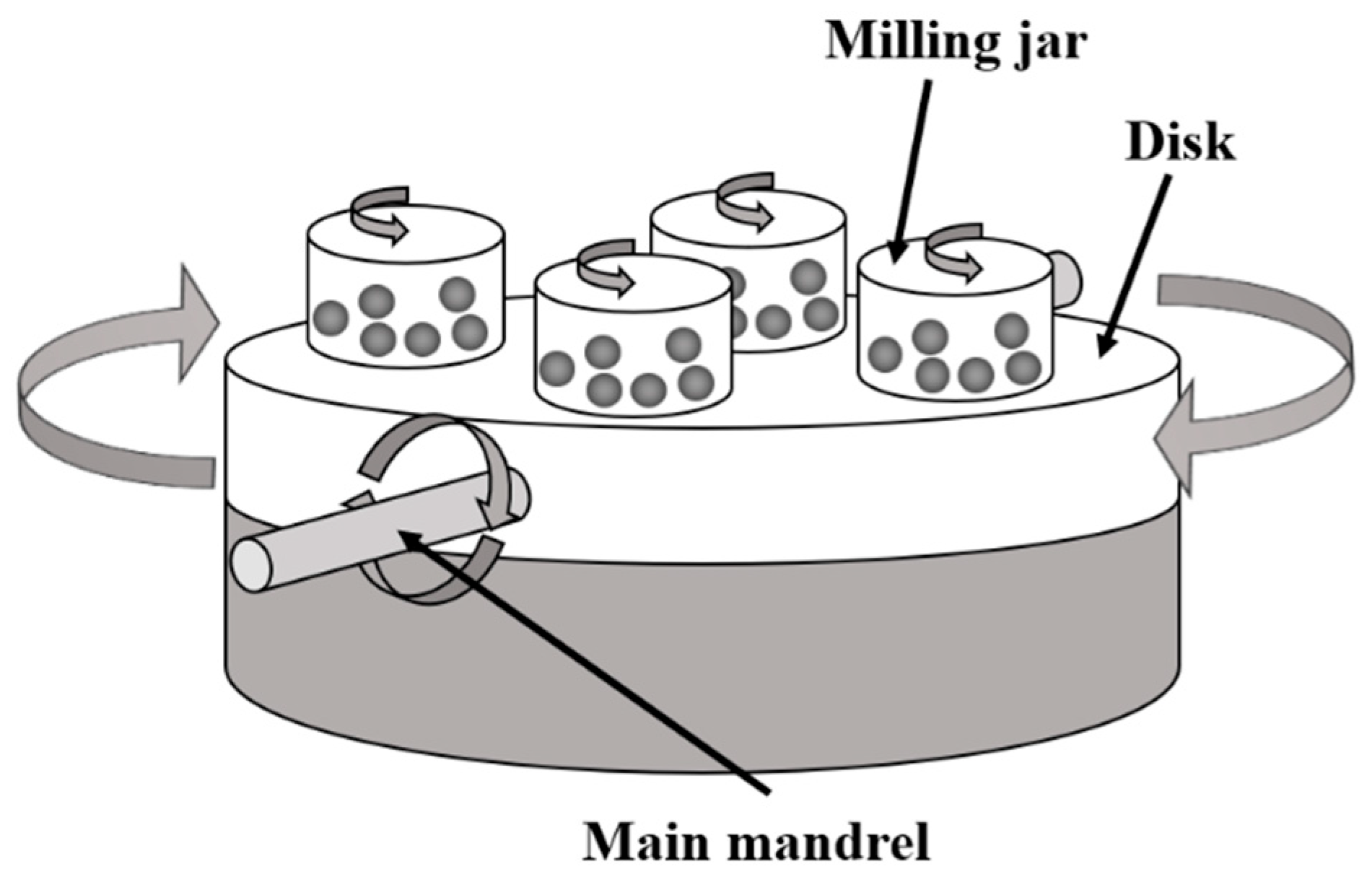
4.2.1. Mechanical Alloying

Mechanical alloying is a solid-state powder processing technique that involves the blending and milling of precursors in a high-energy planetary ball mill, where the process parameters are represented by rotational speed (often from 250 to 800 min−1), process time (from hours to tens of hours depending on the other process parameters), atmosphere (often argon and hydrogen), powder:ball weight ratio (usually from 1:10 to 1:20), and milling media size (diameter from 1 to 10 mm, the choice depends on the starting particles size) [205,206,207]. The vessel and balls can be made of different hard materials; the most common one is stainless steel, but the most effective materials are zirconia (ZrO2) or silicon nitride (Si3N4). When two balls collide, some powder is trapped between them and, depending on the kinetic impact energy, the powder can be broken down to finer particles. The dimensions that can be reached are in the order of hundreds of nanometers; the fine powder can be used to prepare colloidal suspensions or bulk samples via, for example, direct sintering [208,209,210].
As an example, Lin et al. [211] and Lu et al. [212] reduced the particle size of hand-crushed Bi0.45Sb1.55Te3Se0.034 and Bi2Te2.7Se0.3 ingots (initial particle size around 1 mm) to an average of 1 µm with a very short but effective process; they used the Planetary Ball Mill PM100 by Retsch (the schematic of a generic planetary ball milling process is represented in Figure 25). The process consisted in milling with 10 mm diameter stainless steel balls in a vessel of the same material for 30 min at 350 rpm, and successively for 90 min at 350 rpm with 2 mm balls, in both cases with a powder:ball weight ratio of 1:4 and with a 10 min holding time every 20 min of milling to avoid over-heating. The powder was then compressed by cold pressing and finally sintered in argon. Full densification in thermoelectric materials (i.e., intermetallics) after sintering is an issue that is not fully addressed. The equipment used to sinter these materials is often very expensive (e.g., hot isostatic pressing).

4.2.2. Melting

Despite being considered a conventional methodology, melting the mixed raw materials is still largely used to fabricate polycrystalline powders to produce bulk TEMs because of high productivity and scalability, low cost, and ease of operation. The process takes place in an evacuated and sealed quartz tube or container, where the high purity precursor powders are heated up over their melting point and kept at high temperature for a determined amount of time, being finally slowly cooled down to room temperature (cooling can take place also in the presence of oil, water, or liquid N2 to accelerate the process or achieve a particular ingot internal structure) [213,214,215]. Annealing is often carried out after ingot fabrication to increase stability, mechanical properties (ductility, hardness, etc.) and in some cases enhance electrical conductivity and Seebeck coefficient [21,24]. Three different furnaces are largely used in current TEMs manufacturing by melting: high-temperature muffle furnace [32], arc melting method [216,217] (the source is provided by an electrical arc that passes through the precursors, it is used when higher heating rate is required), and melt spinning method [218,219,220] (it consists of hitting an internally cooled cylinder with the molten material stream and it is selected to cool rapidly and achieve precise properties, such as low thickness [196]). A schematic of a generic melting process is shown in Figure 26.
In most cases, the as-fabricated ingots are hand-crushed and used to fabricate bulk samples via single crystal growth (Section 4.1), mechanical alloying (Section 4.2.1), hot pressing or spark plasma sintering (SPS) [24]. Hot pressing (HP) consists of the densification of a weakly packed powder or a compacted preform by simultaneously applying heat and pressure. The attractive features of hot pressing are the possibility to fabricate from small volume samples (tens of mm3) up to samples with higher volumes (tens of cm3), the achievement of high final density, and microstructural improvement (e.g., fine grain size). Hot-pressing procedures include uniaxial hot pressing, continuous pressing, and hot isostatic pressing (HIP). The main disadvantages of these processes are their high cost and limited shape-freedom when producing at high mass rates [224,225,226]. In TEMs manufacturing, the most used techniques among these are uniaxial hot pressing and HIP [24]. However, the most frequently used compaction technology for bulk samples fabrication is spark plasma sintering; this technology is a sintering technique involving the simultaneous use of uniaxial pressure and high-intensity and low-voltage pulsed current [227,228]. SPS can be considered a hot-pressing process where the furnace is replaced by the mold containing the powder, which is heated by a current flowing through it and eventually through the sample. Thanks to its high effectiveness, SPS is used to sinter materials which are normally difficult to compact, such as nanomaterials, refractory materials, and TEMs. The unique features of SPS are the higher heating rates (up to hundreds of K min−1; this enables faster processing considering that for HP the typical rates are in the order of tens of K min−1), shorter sintering cycles, lower sintering temperatures (up to 923–1023 K; low temperatures are allowed by the higher process efficiency, a typical SPS process does not last longer than a few minutes), and reduced grain growth (this is enabled by lower process temperatures and shorter holding time) [225,227,228,229,230,231].

4.3. Film Technologies: Chemical and Physical Methods

Crystalline materials such as nano- and micro-plates, nanowires, and thin films are often prepared using evaporation or deposition methods, which are crucial for the fabrication of miniature or microscale TE devices [232,233,234]. In a typical evaporation or deposition method, the source material or precursors should be evaporated in vacuum or put in a gas (i.e., aerosol), so that the material can travel to the target object (called substrate); finally, the vapors can condense or react on the substrate to form a crystalline solid [232,235,236]. According to a wide collection of literature [37,72,237,238,239,240], manufacturing via evaporation or deposition methods is one of the most promising paths for small scale TEMs fabrication because of the high quality of the final product, the possibility to deposit any material, and the high scalability of the process. However, the two main factors hindering the applicability of these technologies are the difficult optimization of process parameters (thus complicating the achievement of the process reproducibility) and the high process costs (as an example, magnetron sputtering requires a high vacuum chamber to maintain high quality during deposition, high voltage discharges, and highly expensive magnets [241,242,243]). Therefore, research has focused on deposition technologies that can guarantee high quality materials but with lower economic costs [233,234,238,244,245,246,247]; currently, inkjet printing and aerosol jet printing are candidates satisfying such requirements, since a variety of promising cases have been collected in literature [248,249,250]. Aerosol jet printing (AJP) is especially interesting thanks to the possibility of using almost any material dispersed in a liquid phase [251,252,253]. In Section 3.2, Section 3.3 and Section 4.3.1, the deposition technologies mainly used for TEGs fabrication are briefly described along with examples, with a particular focus on AJP.

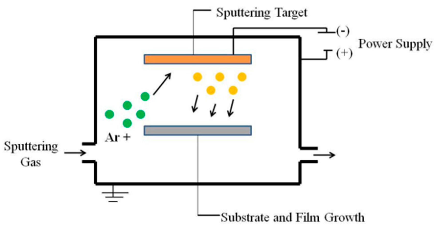
4.3.1. Magnetron Sputtering

Sputtering occurs when an ion impact establishes a train of collisions on the target, leading to the ejection of a matrix atom. Sputtering is related to the transfer of momentum from energetic particles to the target surface atoms. Most of the kinetic energy transferred to the target by incoming ions is converted into heat; therefore, an efficient cooling system is required [254,255]. A generic sputter deposition process consists in the evacuation of a chamber (the pressure ranges from 10−3 to 10−1 mbar) and the discharge is initiated and sustained thanks to an inert gas that fills the chamber (usually argon, and it is also referred as ‘medium’). The target (cathode) is subjected to a negative voltage; subsequently, a current flow and a film is condensed on the substrate (anode). Positive ions in the discharge hit the cathode and eject neutral target atoms; these atoms pass through the discharge region to finally deposit on the growing film. The discharge is sustained by ionization thanks to secondary electrons emitted from the target plate [241,243,254]. A schematic of a generic sputtering deposition process is shown in Figure 27.
Direct current (DC) and radio frequency (RF) sputtering are the two main sputtering deposition modalities; the former is characterized by the application of direct current (voltage up to 800 V), low ionization efficiency, and the suitable pressure range for operation is quite narrow (below 10−2 mbar), whereas the latter is characterized by the utilization of alternate current (from a few kHz to almost 1 GHz; radio frequency range is used as it establishes a total negative voltage and fixed anode and cathode behavior) and higher ionization efficiency [243,254,257]. In magnetron sputtering, a magnetic field is therefore superimposed to the electrical field already present between target and substrate, therefore applying the additional Lorentz force to the electrons. In magnetrons, the ionizing efficiency is increased by the electrons trapped near the target (thanks to a magnetic field oriented parallel to the target and perpendicular to the electric field). Therefore, a closed path for the electrons is defined placing the magnets behind the target. The target erosion by sputtering takes place within this path because the maximum ionization intensity is located above the sputtered material [242,258,259]. Larger discharge currents and increased sputter deposition rates are achieved with magnetron sputtering rather than traditional sputtering technologies [241,242,243] (usually 1 µm/min is attained in RF magnetron sputtering, against the usual 0.5 µm/min of conventional RF sputtering, both considering aluminum as target material [254]). Magnetron sputtering can be applied both in direct current and radio frequency modality, but usually it is applied in RF modality because of the higher deposition rates; it can be used to deposit thin films with thickness from tens of nanometers to tens of micrometers [254,260]. The magnetron sputtering process is shown in Figure 28.
As an example, Kurokawa et al. [262] fabricated a nanocrystalline bismuth telluride thin film via DC magnetron sputtering with a maximum ZT value around 0.7 near room temperature (300 K). They deposited the material on different substrates (BK7 glass, polyimide, alumina, and sapphire, all 125 µm thick) annealing the sample for 2 h at 573 K, obtaining the higher ZT value when deposited on glass. The thin films were characterized by an average crystal size of 20 nm, and the film thickness was around 1 µm. The deposition rate was around 0.4 nm·s−1 and the distance between target (Bi2Te3 disk with 127 mm diameter) and substrate (heated up at 573 K) was 140 mm. The thermoelectric performance of the rapidly fabricated thin films is high; however, since the substrate is of moderate temperature, only materials resistant to such temperature range can be used. Finally, magnetron sputtering is an expensive technology and can be utilized only for niche applications [242,254,258].

4.3.2. Inkjet Printing (IJP)

Inkjet printing (IJP) is a suspension-based, non-contact and additive deposition process in which materials are patterned at high speed (up to 100 mm⸱s−1) and resolution (up to 10 µm), achieving thin films with thicknesses in the order of tens of nanometers [249,263,264]. IJP can be used in two main modalities, continuous (CIJ) and drop-on-demand (DOD) [265]: continuous inkjet printers use plate electrodes to selectively charge individual droplets in a falling jet; charged droplets are deflected by an electric field onto a substrate while uncharged droplets fall into a gutter system for recycling. In drop-on-demand inkjet systems, individual droplets are ejected mainly via piezoelectric actuators [249,263,265].
The formation and displacement of a droplet is imposed through a shockwave on the plastic container. In this case, ink viscosity must be low enough to permit the formation of the drop after the shockwave. After deposition, the solvent is meant to evaporate, leaving on the substrate only the functional part of the ink [248,249,266,267]. DOD printing guarantees higher reliability and precision than CIJ printing but needs more time to print the same feature [265]. The DOD and CIJ systems are depicted in Figure 29.
Chen et al. [250] deposited thin films based on bismuth telluride (Bi2Te3) and bismuth antimony telluride (Bi0.5Sb1.5Te3) nanowires (NWs) through drop-on-demand inkjet printing onto polyimide substrates. The maximum power factor was found at room temperature around 180 µWm−1K−2 and 110 µWm−1K−2 for the Bi2Te3 and Bi0.5Sb1.5Te3 nanowires, respectively. The 8 nm thick nanowires were fabricated via low temperature, solution-phase synthesis methods. Tellurium dioxide with surfactant polyvinylpyrrolidone is reduced into tellurium NWs within a mixture of potassium hydroxide (KOH), ethylene glycol, and hydrazine (N2H4, that works as a reduction agent). Subsequently, bismuth and antimony precursors are added to form the BST and BT NWs, respectively. Finally, the solution was diluted with distilled water to reach low viscosity for printing. The printed thin films had a thickness lower than 5 µm. Samples printed with IJP always necessitate annealing. Chen et al. carried out the annealing at 723 K for 10 min. This treatment significantly increased electrical conductivity of the samples. Despite its relatively low cost and high-quality results, inkjet printing does not enable the printing of any material since a narrow viscosity range should be attained; not only would not respecting such requirements lead to low quality results, but also to machine damages (i.e., clogging and over-heating) [249,265,267].

4.3.3. Aerosol Jet Printing (AJP)

Aerosol jet printing (AJP) is an emerging microscale additive manufacturing technology used to print films on any substrate. Films are deposited by random stacking of layers; this happens due to the spraying nature of the technology [269,270]. AJP is a promising tool for the application of functional nanomaterials to printed electronics (e.g., flexible circuits, environmental and biomedical sensing).
The Inks for AJP are colloidal su”pens’ons, often based on organic or polymeric dispersing phases. The achievable resolution on the substrate can be lower than 10 µm [252,271].
The process requires three gases: atomizing gas (only with pneumatic atomization), carrier gas, and sheath gas. Aerosol jet printing is divided into five main physical steps:
  • Atomization: the functional ink is transformed into an aerosol through pneumatic or ultrasonic atomization.
    Pneumatic atomization: a piston is partially immersed in the ink. Aerosolization is achieved using an atomizing gas (usually N2) that hits the ink through the piston, splashing the droplets.
    Ultrasonic atomization: commercial aerosol jet printers usually use this system. High frequency (MHz) ultrasound sets up a capillary wave on the ink surface, leading droplets to break off with a well-defined size distribution.
  • Transport: following atomization, the carrier gas (often nitrogen N2) carries ink droplets through the mist tube to the deposition head. The process can take around 10 s under typical operating conditions. Large droplets are separated from small droplets before collimation: the large ones go back to the jar; the small ones are part of the aerosol.
  • Collimation: while entering the deposition head, the aerosol gas (which contains ink droplets) is surrounded by a flowing sheath gas (usually N2). This collimates the beam and prevents ink accumulation on the deposition nozzle walls.
  • Aerodynamic focusing: sheath gas allows volume displacement to collimate the aerosol inside the deposition head. Aerodynamic focusing makes it possible to better collimate the aerosol gas. Therefore, the focusing offered by the sheath gas is coupled with the mechanical focusing of the nozzle (the nozzle diameter can vary from 100 to 400 µm).
  • Impact: the aerosol jet hits the substrate, and it gets deposited following a pattern defined in a 2D environment software (e.g., KEWA software for Ceradrop AJ printers). Droplets with a size smaller than average will not impact the substrate; droplets sized larger than the critical dimension will impact the substrate but overspreading on the surface [252,269,272].
The above-mentioned steps are represented in Figure 30.
Key process parameters in AJP are:
  • Ink mass density, ρp (g·cm−3)
  • Ink viscosity, η (cP)
  • Ink surface tension, γs (N·m−1)
  • Atomizer gas flow, FG (sccm)
  • Carrier gas flow, FC (sccm)
  • Sheath gas flow, FS (sccm)
  • Ink temperature, T (K)
  • Deposition nozzle diameter, D (µm)
  • System geometry (e.g., diameter of the mist tube)
  • Deposition velocity, v (mm⸱s−1)
Jet focusing is crucial for the process since during aerosol transportation, droplets colliding with the walls are lost, leading to changes in the deposition rate (material impinging). With experience and practice, it is possible to define an operational window that permits an optimal printing process; this is defined depending on the parameters mentioned above. Material loss can lead to contamination, process drift, and clogging of the printing head. Two main physical mechanisms are the source of transport losses:
  • Gravitational sedimentation: it is generally associated with larger droplets. It consists in settling before deposition of larger droplets during transportation.
  • Diffusion: usually associated with smaller droplets. The loss is due to droplets diffusion after impingement against the tube walls [252,272].
Together with process parameters, these phenomena determine the inertial impaction effectiveness; it is quantified using Stokes number (St), defined as St = ρp⸱U⸱Cc⸱dp2⸱(9⸱µ⸱D)−1; where ρp (g·cm−3) is the ink mass density, U (m·s−1) is the impinging jet velocity, Cc (arb. units) is the Cunningham slip correction factor, dp (µm) droplet diameter, and D (µm) nozzle diameter of the deposition head.
Attention should be focused on the droplet size:
  • Small dp (St < 1): low focusing, diffusion takes place.
  • High dp (St > 1): over-focusing, gravitational sedimentation occurs.
  • Optimal focusing: St ~ 1
Parameter selection should be carried out by coupling this approach with the printing practical experience, aiming to achieve optimal focusing [252,273].
The attractive aspects of AJP in comparison to traditional technologies and other AM technologies (e.g., inkjet printing) for TEMs preparation are:
  • Wide ink viscosity (η) acceptability range (η can range from 1 to 1000 cP for AJ printer installed with pneumatic atomizers), permitting the utilization of different materials.
  • High resolution printing (<5 µm × 5 µm) [274].
  • The thickness range of a single pass layer is from 100 nm to 10 µm. The ink solid fraction is a crucial parameter for this dimension: higher nanoparticles concentration means higher thickness.
  • Simple geometry control thanks to aerosol jet printing systems configuration and to aerodynamic focusing.
  • In comparison to other AM technologies (e.g., inkjet printing), clogging is less likely to take place thanks to the sheath gas utilization.
  • The process is flexible, potentially cheap, and scalable [275,276].
On the other hand, the issues which should be addressed around AJP are:
  • Due to the large number of parameters, defining optimal conditions is a hard and long process. This is also related to the difficult reproducibility of the process.
  • Films often lack homogeneity and property uniformity, and high pore volume fraction (vol%) can be detrimental (in good proportions, porosity is favorable for thermal conductivity reduction, whereas in unfavorable proportions, it is detrimental for electrical conductivity enhancement). Optimal printing conditions can solve such issues.
  • Overspray: the ink is deposited on unintended areas of the substrate, usually around the actual printed material. The problem can be reduced by matching the conditions of optimal focusing.
  • Time-consuming cleaning and maintenance of the printer can be crucial. It must be carried out after every printing session [251,252].
Currently, research is in its preliminary state, forcing a step-by-step approach. A literature review of bismuth telluride-based aerosol jet printing thermoelectric devices is presented in Section 5.1 Bismuth telluride is selected thanks to the high performances in the low temperature range, together with its current position in the market, as summarized in Section 3.8. However, bismuth telluride is extremely sensitive to oxidation, forcing the utilization of non-aqueous-based suspensions. Both inkjet printing and aerosol jet printing are less performing with inks based on organic carriers because of the lower surface tension than water.
In conclusion, aerosol jet printing is a promising technology for the fabrication of solid-state generators; flexibility, scalability, and possible low costs are encouraging aspects.

5. Conclusions

5.1. Printing of Bismuth Telluride-Based Thermoelectric (BT-TE) Materials through Aerosol Jet Printing (AJP)

Research works about AJP of BT-TEMs are not numerous because of the recent development of the technique. However, the fabrication path described in the different papers is similar, as represented in Figure 31.
It is important to point out that powders are mostly prepared by chemical synthesis; high energy ball milling is instead widely used to prepare BT-TE powders for compacted samples fabrication but not for additive manufacturing technologies.
As an example, Hollar et al. [253] deposited Bi2Te3 thin films on flexible polyimide (PI) substrates using aerosol jet printing. The thin films fabricated by the group showed a peak power factor value of 0.35 mWm−1K−2 at 473 K. Inks were prepared by solution-phase synthesis of Bi2Te3 nanoplatelets: Bi(NO3)3⸱5H2O (bismuth nitrate), NaTeO3 (sodium tellurite), NaOH (sodium hydroxide), PVP (polyvinylpyrrolidone), and EG (ethylene glycol) were used. The thin films thickness (always in the order of hundreds of nanometers) was tunable depending on the nanoplatelets concentration: the higher the concentration, the higher the thickness. The printer aerosolized the ink with an ultrasonic system. The key process parameters were:
  • Platen temperature: 313 K
  • Carrier gas flow: 35 sccm
  • Nozzle diameter: 200 µm
  • Stand-off: 3 mm
The samples were dried in a glovebox after printing, then sintering was carried out at 623 K for 1 h in Argon atmosphere.
A couple of thin films deposited on the flexible substrate by Hollar et al. are shown in Figure 32, together with a scanning transmission electron microscope (STEM) cross-sectional image. The film was porous and showed few inhomogeneities; during aerosol jet printing, this is the main issue with the finished product. The solution is optimization as well as the process parameters.
Tony Varghese [277] developed his PhD thesis about n-type bismuth telluride films fabricated with additive manufacturing. Varghese et al. achieved a power factor value equal to 250 µWm−1K−2 at room temperature. He chemically synthesized Bi2Se0.3Te2.7 nanoparticles (NPs) via microwave-assisted stimulated wet-chemical method.
During chemical synthesis, thiolglycolic acid (TGA) is added to have a capping effect on the NPs. The ink was prepared as a 60 wt%/40 wt% mixture of nanoparticles and dispersing phase.
The dispersing phase was a mixture of ethylene glycol:glycerol:ethanol (35:5:60 wt%). The printer was equipped with a pneumatic system for aerosolization; this allows the processing of high viscosity inks with high solid fractions. The printing was carried out on an oxygen plasma-treated HN Kapton substrate.
The printing parameters were:
  • Platen temperature: 348 K
  • Carrier gas flow (N2): 470 sccm
  • Nozzle diameter: 300 µm
  • Stand-off: 3 mm
Again, the thickness of the thin films was in the order of hundreds of nanometers. Drying was carried out on a hot plate at 473 K for 5 min. However, some samples were pressed hydraulically, and others were not pressed; the effect on porosity, thermoelectric properties, and thickness was studied. Porosity was reduced by 40%, as well as thickness. A slight improvement in TE was detected. Photonic sintering was carried out on the samples: a xenon lamp ranged from 200 to 800 nm of wavelength. Based on the sample, treatment could last from few minutes to tens of minutes.
Other works in literature [278,279] could be mentioned as examples.
Aerosol jet printing of films using BT-TE inks prepared starting from milled powders has never been mentioned in literature. However, numerous papers demonstrate that mechanical alloying can be used to prepare doped bismuth telluride nano-powders [185,211,280,281]. Once the powder is prepared, it can be dispersed in a liquid phase, thus proceeding with printing. The reduction of the powder mean size in the sub-micrometric range by ball miling is still to be achieved. It is generally difficult to reduce the mean size to under 1 µm. The process is well explained in Section 4.2.1, together with an example.
As a further example, Kim et al. [280] prepared a BT-TE ink for inkjet printing using high energy ball milling. In that case, they prepared p-type Bi0.4Sb1.6Te3 and n-type Bi2Sb1.6Se0.3 powders by mechanical alloying. High energy ball milling was carried out with Bi, Te, Se, and Sb in stoichiometric ratio for 5 h, reaching a grain size lower than 45 µm. As dispersing phase for inkjet printing, glycerol was used.
The works by Li et al. [282] and Yang et al. [281] are further examples of BT-TE powder preparation and deposition.

5.2. Final Remarks

This review highlights the superiority of bismuth telluride-based materials for moderate temperature applications thanks to ease of fabrication, low cost in comparison to other high performing TEMs (e.g., SKUs), and high performances (ZT up to 1.3 at RT) [22,23,32,98]. Furthermore, the enormous potential of aerosol jet printing for TEMs fabrication was highlighted: scalability (e.g., clogging less likely to happen), flexibility (e.g., wide viscosity range), and low price (e.g., fast printing) are encouraging aspects [275,276]. However, limiting factors hinder the development of a suitable approach to fabricate BT-TE materials on an industrial scale using this spraying technology. The main difficulties deal with ink formulation (viscosity η (cP) and surface tension γ (N⸱m−1): nanoparticles volume fraction and deflocculant chemistry and amount) and printing parameters (i.e., atomizer FG, carrier FC, and sheath gas FS flows (sccm), and printing temperature T (K)); defining an operating window is still a complex task [251,252].
Currently, suspensions for aerosol jet printing are prepared via dispersion using chemically synthesized BT-TE powders. Chemical synthesis guarantees high control on NPs size and composition, but it is not scalable: low volumes and high prices [253,277]. However, in literature, it was demonstrated that it is possible to prepare BT-TE NPs using high energy ball milling (i.e., mechanical alloying). This process does guarantee similar powder quality to chemical synthesis, but it is more scalable: lower price and higher volumes [211,281]. Research works about the AJP of BT-TE inks prepared via high energy ball milling are not yet present in the literature.
In view of a more environmentally friendly and sustainable industry of thermoelectric materials, we think that studying the combination of powder processing, and aerosol jet printing might be promising for the future.
Therefore, the preparation of inks for AJP starting from milled powders should be considered for future research; in practice, two main paths should be followed:
  • AJP process optimization: achieving process reproducibility would enable the definition of process windows depending on ink formulation.
  • Utilization of BT-TE inks prepared from powder synthesized by high energy ball milling: this would couple innovation with future process scalability.

Funding

This research was funded by STMicroelectronics S.R.L.

Conflicts of Interest

The authors declare no conflict of interest.

References

  1. Mamur, H.; Bhuiyan, M.R.A.; Korkmaz, F.; Nil, M. A Review on Bismuth Telluride (Bi2Te3) Nanostructure for Thermoelectric Applications. Renew. Sustain. Energy Rev. 2018, 82, 4159. [Google Scholar] [CrossRef]
  2. Sajid, M.; Hassan, I.; Rahman, A. An Overview of Cooling of Thermoelectric Devices. Renew. Sustain. Energy Rev. 2017, 78, 15. [Google Scholar] [CrossRef]
  3. Gupta, M. Review on Heat Recovery Unit with Thermoelectric Generators. Power 2014, 4, 2021. [Google Scholar]
  4. Narducci, M.; Castellero, D.; Fanciulli, A.; Puglia, C.; Gobbato, F.; Bennetti, P. Materiali Termoelettrici e Tecnologie per Il Recupero di Calore Disperso, in Materiali Termoelettrici e Tecnologie per Il Recupero di Calore Disperso-Associazione Italiana Metallurigia (AIM) (2021), p. 2021. Available online: https://www.aimnet.it/manifestazione.php?id=698&idc= (accessed on 13 June 2023).
  5. Polozine, A.; Sirotinskaya, S.; Schaeffer, L. History of Development of Thermoelectric Materials for Electric Power Generation and Criteria of Their Quality. Mater. Res. 2014, 17, 1260. [Google Scholar] [CrossRef]
  6. Siddique, A.R.M.; Mahmud, S.; Van Heyst, B. A Review of the State of the Science on Wearable Thermoelectric Power Generators (TEGs) and Their Existing Challenges. Renew. Sustain. Energy Rev. 2017, 73, 730. [Google Scholar] [CrossRef]
  7. Burmester, D.; Rayudu, R.; Seah, W.; Akinyele, D. A Review of Nanogrid Topologies and Technologies. Renew. Sustain. Energy Rev. 2017, 67, 760. [Google Scholar] [CrossRef]
  8. Schwall, M.; Balke, B. Phase separation as a key to a thermoelectric high efficiency. Phys. Chem. Chem. Phys. 2012, 15, 1868–1872. [Google Scholar] [CrossRef] [PubMed]
  9. Champier, D. Thermoelectric generators: A review of applications. Energy Convers. Manag. 2017, 140, 167–181. [Google Scholar] [CrossRef]
  10. Dehkordi, A.M.; Zebarjadi, M.; He, J.; Tritt, T.M. Thermoelectric Power Factor: Enhancement Mechanisms and Strategies for Higher Performance Thermoelectric Materials. Mater. Sci. Eng. R Rep. 2015, 97, 1. [Google Scholar] [CrossRef]
  11. Bell, L.E. Cooling, Heating, Generating Power, and Recovering Waste Heat with Thermoelectric Systems. Science 2008, 321, 1457–1461. [Google Scholar] [CrossRef]
  12. Yan, X.; Liu, W.; Wang, H.; Chen, S.; Shiomi, J.; Esfarjani, K.; Wang, H.; Wang, D.; Chen, G.; Ren, Z. Stronger phonon scattering by larger differences in atomic mass and size in p-type half-Heuslers Hf1−xTixCoSb0.8Sn0.2. Energy Environ. Sci. 2012, 5, 7543–7548. [Google Scholar] [CrossRef]
  13. Kempf, N.; Zhang, Y. Design and Optimization of Automotive Thermoelectric Generators for Maximum Fuel Efficiency Improvement. Energy Convers. Manag. 2016, 121, 224. [Google Scholar] [CrossRef]
  14. Ahiska, R.; Mamur, H. Development and Application of a New Power Analysis System for Testing of Geothermal Thermoelectric Generators. Int. J. Green Energy 2016, 13, 672. [Google Scholar] [CrossRef]
  15. He, R.; Schierning, G.; Nielsch, K. Thermoelectric Devices: A Review of Devices, Architectures, and Contact Optimization. Adv. Mater. Technol. 2018, 3, 1700256. [Google Scholar] [CrossRef]
  16. Mamur, H.; Ahiska, R. Application of a DC-DC Boost Converter with Maximum Power Point Tracking for Low Power Thermoelectric Generators. Energy Convers. Manag. 2015, 97, 265. [Google Scholar] [CrossRef]
  17. Rausch, E.; Balke, B.; Deschauer, T.; Ouardi, S.; Felser, C. Charge Carrier Concentration Optimization of Thermoelectric P-Type Half-Heusler Compounds. APL Mater. 2015, 3, 041516. [Google Scholar] [CrossRef]
  18. Huen, P.; Daoud, W.A. Advances in Hybrid Solar Photovoltaic and Thermoelectric Generators. Renew. Sustain. Energy Rev. 2017, 72, 1295. [Google Scholar] [CrossRef]
  19. Hossain, S.; Li, T.; Yu, Y.; Yong, J.; Bahk, J.-H.; Skafidas, E. Recent advances in printable thermoelectric devices: Materials, printing techniques, and applications. RSC Adv. 2020, 10, 8421–8434. [Google Scholar] [CrossRef]
  20. Wei, J.; Yang, L.; Ma, Z.; Song, P.; Zhang, M.; Ma, J.; Yang, F.; Wang, X. Review of current high-ZT thermoelectric materials. J. Mater. Sci. 2020, 55, 12642–12704. [Google Scholar] [CrossRef]
  21. Jaziri, N.; Boughamoura, A.; Müller, J.; Mezghani, B.; Tounsi, F.; Ismail, M. A Comprehensive Review of Thermoelectric Generators: Technologies and Common Applications. Energy Rep. 2020, 6, 264. [Google Scholar] [CrossRef]
  22. Rowe, D. Thermoelectrics and Its Energy Harvesting; CRC Press: Boca Raton, FL, USA, 2012. [Google Scholar]
  23. Rowe, D.M. Thermoelectrics Handbook Macro to Nano; Rowe, D.M., Ed.; CRC Press: Boca Raton, FL, USA, 2006. [Google Scholar]
  24. Shi, X.L.; Zou, J.; Chen, Z.G. Advanced Thermoelectric Design: From Materials and Structures to Devices. Chem. Rev. 2020, 120, 7399. [Google Scholar] [CrossRef] [PubMed]
  25. Thermoelectric Materials Market By Product Type, By Distribution Channel, By Application, Forecasts to 2027. Available online: https://www.emergenresearch.com/industry-report/thermoelectric-materials-market (accessed on 13 June 2023).
  26. Li, K.; Garrison, G.; Zhu, Y.; Horne, R.; Petty, S. Cost Estimation of Thermoelectric Generators, 46th Work. Geotherm. Reserv. Eng. 2021, 1, 3–5. [Google Scholar]
  27. Karthick, K.; Suresh, S.; Hussain, M.M.M.; Ali, H.M.; Kumar, C.S. Evaluation of solar thermal system configurations for thermoelectric generator applications: A critical review. Sol. Energy 2019, 188, 111–142. [Google Scholar] [CrossRef]
  28. Ahiska, R.; Dislitas, S.; Omer, G. A new method and computer-controlled system for measuring the time constant of real thermoelectric modules. Energy Convers. Manag. 2012, 53, 314–321. [Google Scholar] [CrossRef]
  29. Harman, T.C.; Taylor, P.J.; Walsh, M.P.; LaForge, B.E. Quantum Dot Superlattice Thermoelectric Materials and Devices. Science 2002, 297, 2229. [Google Scholar] [CrossRef]
  30. Joshi, G.; He, R.; Engber, M.; Samsonidze, G.; Pantha, T.; Dahal, E.; Dahal, K.; Yang, J.; Lan, Y.; Kozinsky, B.; et al. NbFeSb-Based p-Type Half-Heuslers for Power Generation Applications. Energy Environ. Sci. 2014, 7, 4070. [Google Scholar] [CrossRef]
  31. Siouane, S.; Jovanović, S.; Poure, P. Fully Electrical Modeling of Thermoelectric Generators with Contact Thermal Resistance Under Different Operating Conditions. J. Electron. Mater. 2017, 46, 40. [Google Scholar] [CrossRef]
  32. Shi, Y.; Sturm, C.; Kleinke, H. Chalcogenides as thermoelectric materials. J. Solid State Chem. 2019, 270, 273–279. [Google Scholar] [CrossRef]
  33. Hicks, L.D.; Dresselhaus, M.S. Effect of quantum-well structures on the thermoelectric figure of merit. Phys. Rev. B 1993, 47, 12727–12731. [Google Scholar] [CrossRef]
  34. Hicks, L.D.; Dresselhaus, M.S. Thermoelectric figure of merit of a one-dimensional conductor. Phys. Rev. B 1993, 47, 16631–16634. [Google Scholar] [CrossRef]
  35. Liu, W.; Ren, Z.; Chen, G. Nanostructured Thermoelectric Materials. Springer Ser. Mater. Sci. 2013, 182, 255. [Google Scholar]
  36. Chen, Z.-G.; Han, G.; Yang, L.; Cheng, L.; Zou, J. Nanostructured thermoelectric materials: Current research and future challenge. Prog. Nat. Sci. Mater. Int. 2012, 22, 535. [Google Scholar] [CrossRef]
  37. Liu, D.W.; Li, J.F.; Chen, C.; Zhang, B.P.; Li, L. Fabrication and Evaluation of Microscale Thermoelectric Modules of Bi2Te3-Based Alloys. J. Micromechanics Microengineering 2010, 20, 125031. [Google Scholar] [CrossRef]
  38. Ashalley, E.; Chen, H.; Tong, X.; Li, H.; Wang, Z.M. Bismuth telluride nanostructures: Preparation, thermoelectric properties and topological insulating effect. Front. Mater. Sci. 2015, 9, 103–125. [Google Scholar] [CrossRef]
  39. Goldsmid, H.J. Bismuth Telluride and Its Alloys as Materials for Thermoelectric Generation. Materials 2014, 7, 2577–2592. [Google Scholar] [CrossRef]
  40. Liu, S.; Hu, B.; Liu, D.; Li, F.; Li, J.-F.; Li, B.; Li, L.; Lin, Y.-H.; Nan, C.-W. Micro-thermoelectric generators based on through glass pillars with high output voltage enabled by large temperature difference. Appl. Energy 2018, 225, 600–610. [Google Scholar] [CrossRef]
  41. Li, J.-F.; Tanaka, S.; Umeki, T.; Sugimoto, S.; Esashi, M.; Watanabe, R. Microfabrication of thermoelectric materials by silicon molding process. Sens. Actuators A Phys. 2003, 108, 97–102. [Google Scholar] [CrossRef]
  42. Kao, P.-H.; Shih, P.-J.; Dai, C.-L.; Liu, M.-C. Fabrication and Characterization of CMOS-MEMS Thermoelectric Micro Generators. Sensors 2010, 10, 1315. [Google Scholar] [CrossRef]
  43. Dhawan, R.; Madusanka, P.; Hu, G.; Debord, J.; Tran, T.; Maggio, K.; Edwards, H.; Lee, M. Si0.97Ge0.03 Microelectronic Thermoelectric Generators with High Power and Voltage Densities. Nat. Commun. 2020, 11, 4362. [Google Scholar] [CrossRef]
  44. Hu, G.; Edwards, H.; Lee, M. Silicon integrated circuit thermoelectric generators with a high specific power generation capacity. Nat. Electron. 2019, 2, 300–306. [Google Scholar] [CrossRef]
  45. Thelemann, T.; Thust, H.; Hintz, M. Using LTCC for microsystems. Microelectron. Int. 2002, 19, 19–23. [Google Scholar] [CrossRef]
  46. Markowski, P.M. Multilayer thick-film thermoelectric microgenerator based on LTCC technology. Microelectron. Int. 2016, 33, 155–161. [Google Scholar] [CrossRef]
  47. Park, T.; Lim, H.; Hwang, J.U.; Na, J.; Lee, H.; Kim, E. Roll Type Conducting Polymer Legs for Rigid-Flexible Thermoelectric Generator. APL Mater. 2017, 5, 074106. [Google Scholar] [CrossRef]
  48. Zhu, J.; Xu, Z.; Jia, L. Design and Fabrication of 3D Flexible Thermoelectric Energy Generator Using Chemical Vapor Deposition Method Based on Paper Substrate. In Proceedings of the 2018 International Symposium in Sensing and Instrumentation in IoT Era (ISSI), Shanghai, China, 5–6 September 2018; pp. 1–4. [Google Scholar]
  49. Grishin, V.I. Method for Manufacturing Semiconductive Branches for a Thermoelectric Module, and Thermoelectric Module. US Patent 20170012195, 24 February 2014. [Google Scholar]
  50. Crane, D.T.; Lagrandeur, J.W. Progress Report on BSST-Led US Department of Energy Automotive Waste Heat Recovery Program. J. Electron. Mater. 2010, 39, 2142. [Google Scholar] [CrossRef]
  51. Orr, B.; Akbarzadeh, A.; Lappas, P. An exhaust heat recovery system utilising thermoelectric generators and heat pipes. Appl. Therm. Eng. 2017, 126, 1185–1190. [Google Scholar] [CrossRef]
  52. Nozariasbmarz, A.; Kishore, R.A.; Poudel, B.; Saparamadu, U.; Li, W.; Cruz, R.; Priya, S. High Power Density Body Heat Energy Harvesting. ACS Appl. Mater. Interfaces 2019, 11, 40107. [Google Scholar] [CrossRef]
  53. Torfs, T.; Leonov, V.; Vullers, R.J.M. Pulse Oximeter Fully Powered by Human Body Heat. Senosors Transducers J. 2007, 80, 1230. [Google Scholar]
  54. Torfs, T.; Leonov, V.; Yazicioglu, R.F.; Merken, P.; Van Hoof, C.; Vullers, R.J.M.; Gyselinckx, B. Wearable Autonomous Wireless Electro-Encephalography System Fully Powered by Human Body Heat. Proc. IEEE Sens. 2008, 2008, 1269. [Google Scholar]
  55. Patidar, S. Applications of Thermoelectric Energy: A Review. Int. J. Res. Appl. Sci. Eng. Technol. 2018, 6, 1992–1996. [Google Scholar] [CrossRef]
  56. Merriam-Webster, Oximeter Definition & Meaning—Merriam-Webster. Available online: https://www.merriam-webster.com/dictionary/oximeter (accessed on 13 June 2023).
  57. Leonov, V.; van Andel, Y.; Wang, Z.; Vullers, R.J.M.; van Hoof, C. Micromachined Polycrystalline Si Thermopiles in a T-Shirt. Sens. Transducers 2011, 127, 15. [Google Scholar]
  58. Liu, Y.; Yin, L.; Zhang, W.; Wang, J.; Hou, S.; Wu, Z.; Zhang, Z.; Chen, C.; Li, X.; Ji, H.; et al. A Wearable Real-Time Power Supply with a Mg3Bi2-Based Thermoelectric Module. Cell Reports Phys. Sci. 2021, 2, 100412. [Google Scholar] [CrossRef]
  59. Dilhac, J.-M.; Monthéard, R.; Bafleur, M.; Boitier, V.; Durand-Estèbe, P.; Tounsi, P. Implementation of Thermoelectric Generators in Airlinersfor Powering Battery-Free Wireless Sensor Networks. J. Electron. Mater. 2014, 43, 2444. [Google Scholar] [CrossRef]
  60. Iezzi, B.; Ankireddy, K.; Twiddy, J.; Losego, M.D.; Jur, J.S. Printed, Metallic Thermoelectric Generators Integrated with Pipe Insulation for Powering Wireless Sensors. Appl. Energy 2017, 208, 758. [Google Scholar] [CrossRef]
  61. Lin, Q.; Chen, Y.C.; Chen, F.; DeGanyar, T.; Yin, H. Design and Experiments of a Thermoelectric-Powered Wireless Sensor Network Platform for Smart Building Envelope. Appl. Energy 2022, 305, 117791. [Google Scholar] [CrossRef]
  62. Wang, W.; Cionca, V.; Wang, N.; Hayes, M.; O′Flynn, B.; O′Mathuna, C. Thermoelectric Energy Harvesting for Building Energy Management Wireless Sensor Networks. Int. J. Distrib. Sens. Netw. 2013, 2013, 9. [Google Scholar] [CrossRef]
  63. Lineykin, S.; Sitbon, M.; Kuperman, A. Design and optimization of low-temperature gradient thermoelectric harvester for wireless sensor network node on water pipelines. Appl. Energy 2021, 283, 116240. [Google Scholar] [CrossRef]
  64. Shen, Z.-G.; Tian, L.-L.; Liu, X. Automotive exhaust thermoelectric generators: Current status, challenges and future prospects. Energy Convers. Manag. 2019, 195, 1138–1173. [Google Scholar] [CrossRef]
  65. Wu, Z.; Zhang, S.; Liu, Z.; Mu, E.; Hu, Z. Thermoelectric converter: Strategies from materials to device application. Nano Energy 2021, 91, 106692. [Google Scholar] [CrossRef]
  66. Temizer, I.; Ílkılıç, C. The performance and analysis of the thermoelectric generator system used in diesel engines. Renew. Sustain. Energy Rev. 2016, 63, 141–151. [Google Scholar] [CrossRef]
  67. Yu, C.; Chau, K. Thermoelectric automotive waste heat energy recovery using maximum power point tracking. Energy Convers. Manag. 2009, 50, 1506–1512. [Google Scholar] [CrossRef]
  68. LaGrandeur, J. Automotive Waste Heat Conversion to Electric Power Using Skutterudites, TAGS, PbTe and Bi2Te3 Discussion Outline Discussion Outline Background Program Information and System Architecture System Modeling (Bumper to Bumper Vehicle Model Inclusive of Ther, 1 (2006). Available online: https://www1.eere.energy.gov/vehiclesandfuels/pdfs/merit_review_2010/solid-state_energy_conv/ace051_lagrandeur_2010_o.pdf (accessed on 13 June 2023).
  69. Fernández-Yáñez, P.; Armas, O.; Kiwan, R.; Stefanopoulou, A.G.; Boehman, A.L. A Thermoelectric Generator in Exhaust Systems of Spark-Ignition and Compression-Ignition Engines. A Comparison with an Electric Turbo-Generator. Appl. Energy 2018, 229, 80. [Google Scholar] [CrossRef]
  70. Furlong, R.R.; Wahlquist, E.J.U.S. Space Missions Using Radioisotope Power Systems. Nucl. News 1999, 42, 26–35. [Google Scholar]
  71. Streb, A.J. Radioisotope Power Systems for Manned Space Stations Presented as Preprint 64-711 at the AIAA Third Biennial Aerospace Power Systems Conference, Philadelphia, PA, 1–4 September 1964; Academic Press Inc.: Cambridge, MA, USA, 1966; Volume 16. [Google Scholar]
  72. Pourkiaei, S.M.; Ahmadi, M.H.; Sadeghzadeh, M.; Moosavi, S.; Pourfayaz, F.; Chen, L.; Yazdi, M.A.P.; Kumar, R. Thermoelectric Cooler and Thermoelectric Generator Devices: A Review of Present and Potential Applications, Modeling and Materials. Energy 2019, 186, 115849. [Google Scholar] [CrossRef]
  73. Wang, X.; Liang, R.; Fisher, P.; Chan, W.; Xu, J. Critical Design Features of Thermal-Based Radioisotope Generators: A Review of the Power Solution for Polar Regions and Space. Renew. Sustain. Energy Rev. 2020, 119, 109572. [Google Scholar] [CrossRef]
  74. Hammel, T.E.; Bennett, R.; Otting, W.; Fanale, S. Multi-Mission Radioisotope Thermoelectric Generator (MMRTG) and Performance Prediction Model. In Proceedings of the 7th International Energy Conversion Engineering Conference, Denver, Colorado, 2–5 August 2009. [Google Scholar]
  75. Bennett, G.L.; Whitmore, C.W.; Amos, W.R. On the Development of the Power Sources for the Ulysses and Galileo Missions; European Space Agency: Paris, France, 1989. [Google Scholar]
  76. O’Brien, R.C.; Ambrosi, R.M.; Bannister, N.P.; Howe, S.D.; Atkinson, H.V. Safe Radioisotope Thermoelectric Generators and Heat Sources for Space Applications. J. Nucl. Mater. 2008, 377, 506. [Google Scholar] [CrossRef]
  77. Holgate, T.C.; Bennett, R.; Hammel, T.; Caillat, T.; Keyser, S.; Sievers, B. Increasing the Efficiency of the Multi-Mission Radioisotope Thermoelectric Generator. J. Electron. Mater. 2015, 44, 1814. [Google Scholar] [CrossRef]
  78. Zhou, Y.; Paul, S.; Bhunia, S. Harvesting Wasted Heat in a Microprocessor Using Thermoelectric Generators: Modeling, Analysis and Measurement. In Proceedings of the 2008 Design, Automation and Test in Europe, Munich, Germany, 10–14 March 2008. [Google Scholar]
  79. Wang, H.C.; Jewell-Larsen, N.E.; Mamishev, A.V. Thermal Management of Microelectronics with Electrostatic Fluid Accelerators. Appl. Therm. Eng. 2013, 51, 190. [Google Scholar] [CrossRef]
  80. Solbrekken, G.L.; Yazawa, K.; Bar-Cohen, A. Thermal Management of Portable Electronic Equipment Using Thermoelectric Energy Conversion. Thermomechanical Phenom. Electron. Syst. Proc. Intersoc. Conf. 2004, 1, 276. [Google Scholar]
  81. Huang, I.Y.; Lin, J.C.; She, K.D.; Li, M.C.; Chen, J.H.; Kuo, J.S. Development of Low-Cost Micro-Thermoelectric Coolers Utilizing MEMS Technology. Sensors Actuators A Phys. 2008, 148, 176. [Google Scholar] [CrossRef]
  82. Chen, Y.-W.; Wu, C.-C.; Hsu, C.-C.; Dai, C.-L. Fabrication and Testing of Thermoelectric CMOS-MEMS Microgenerators with CNCs Film. Appl. Sci. 2018, 8, 1047. [Google Scholar] [CrossRef]
  83. Kuang, N.; Zuo, Z.; Wang, W.; Liu, R.; Zhao, Z. Optimized thermoelectric properties and geometry parameters of annular thin-film thermoelectric generators using n-type Bi2Te2.7Se0.3 and p-type Bi0.5Sb1.5Te3 thin films for energy harvesting. Sens. Actuators A Phys. 2021, 332, 113030. [Google Scholar] [CrossRef]
  84. Kobayashi, A.; Konagaya, R.; Tanaka, S.; Takashiri, M. Optimized structure of tubular thermoelectric generators using n-type Bi2Te3 and p-type Sb2Te3 thin films on flexible substrate for energy harvesting. Sens. Actuators A Phys. 2020, 313, 112199. [Google Scholar] [CrossRef]
  85. Jeong, S.H.; Cruz, F.J.; Chen, S.; Gravier, L.; Liu, J.; Wu, Z.; Hjort, K.; Zhang, S.; Zhang, Z. Stretchable Thermoelectric Generators Metallized with Liquid Alloy. ACS Appl. Mater. Interfaces 2017, 9, 15791–15797. [Google Scholar] [CrossRef]
  86. Nie, G.; Suzuki, S.; Tomida, T.; Sumiyoshi, A.; Ochi, T.; Mukaiyama, K.; Kikuchi, M.; Guo, J.Q.; Yamamoto, A.; Obara, H. Performance of Skutterudite-Based Modules. J. Electron. Mater. 2017, 46, 2640. [Google Scholar] [CrossRef]
  87. Nam, W.H.; Cho, J.Y. A Brief Review of CoSb3-Based Thermoelectric Materials and Modules for Mid-Temperature Power Generation. Ceramist 2021, 24, 213. [Google Scholar] [CrossRef]
  88. Chen, L.; Zeng, X.; Tritt, T.M.; Poon, S.J. Half-Heusler Alloys for Efficient Thermoelectric Power Conversion. J. Electron. Mater. 2016, 45, 5554. [Google Scholar] [CrossRef]
  89. Dolyniuk, J.-A.; Owens-Baird, B.; Wang, J.; Zaikina, J.V.; Kovnir, K. Clathrate thermoelectrics. Mater. Sci. Eng. R Rep. 2016, 108, 1–46. [Google Scholar] [CrossRef]
  90. Christensen, M.; Johnsen, S.; Iversen, B.B. Thermoelectric clathrates of type I. Dalton Trans. 2009, 39, 978–992. [Google Scholar] [CrossRef]
  91. Zheng, L.; Li, W.; Sun, C.; Shi, X.; Zhang, X.; Pei, Y. Ternary thermoelectric AB2C2 Zintls. J. Alloys Compd. 2019, 821, 153497. [Google Scholar] [CrossRef]
  92. Wang, X.; Li, J.; Wang, C.; Zhou, B.; Zheng, L.; Gao, B.; Chen, Y.; Pei, Y. Orbital Alignment for High Performance Thermoelectric YbCd2Sb2 Alloys. Chem. Mater. 2018, 30, 5339. [Google Scholar] [CrossRef]
  93. Kumar, S.R.S.; Cha, D.; Alshareef, H.N. Lattice dynamics and substrate-dependent transport properties of (In, Yb)-doped CoSb3 skutterudite thin films. J. Appl. Phys. 2011, 110, 083710. [Google Scholar] [CrossRef]
  94. Basu, R.; Singh, A. High temperature Si–Ge alloy towards thermoelectric applications: A comprehensive review. Mater. Today Phys. 2021, 21, 100468. [Google Scholar] [CrossRef]
  95. Xie, K.; Gupta, M.C. High-Temperature Thermoelectric Energy Conversion Devices Using Si-Ge Thick Films Prepared by Laser Sintering of Nano/Micro Particles. IEEE Trans. Electron Devices 2020, 67, 2113–2119. [Google Scholar] [CrossRef]
  96. Toshima, N.; Ichikawa, S. Conducting Polymers and Their Hybrids as Organic Thermoelectric Materials. J. Electron. Mater. 2014, 44, 384–390. [Google Scholar] [CrossRef]
  97. Toshima, N. Recent progress of organic and hybrid thermoelectric materials. Synth. Met. 2017, 225, 3–21. [Google Scholar] [CrossRef]
  98. Furdyna, J.K.; Dong, S.N.; Lee, S.; Liu, X.; Dobrowolska, M. The Ubiquitous Nature of Chalcogenides in Science and Technology; Elsevier Ltd.: Amsterdam, The Netherlands, 2019. [Google Scholar]
  99. Rogl, G.; Rogl, P. Skutterudites, a most promising group of thermoelectric materials. Curr. Opin. Green Sustain. Chem. 2017, 4, 50–57. [Google Scholar] [CrossRef]
  100. Izumi, K.M.F. VESTA 3 for Three-Dimensional Visualization of Crystal, Volumetric and Morphology Data. J. Appl. Cryst. 2011, 44, 1272–1276. [Google Scholar]
  101. Holgate, T.C.; Song, Y.; Bennett, R.; Keyser, S.; Hammel, T.; Siever, R.; Caillat, T.; Fleurial, J.P. Enhancement of the Multi-Mission Radioisotope Thermoelectric Generator with Efficient Skutterudite Thermoelectric Couples: Current Status of the Skutterudite Technology Maturation Program. In Proceedings of the 14th International Energy Conversion Engineering Conference, Salt Lake City, UT, USA, 25–27 July 2016; p. 1. [Google Scholar]
  102. Salvador, J.R.; Waldo, R.A.; Wong, C.A.; Tessema, M.; Brown, D.N.; Miller, D.J.; Wang, H.; Wereszczak, A.A.; Cai, W. Thermoelectric and mechanical properties of melt spun and spark plasma sintered n-type Yb- and Ba-filled skutterudites. Mater. Sci. Eng. B 2013, 178, 1087–1096. [Google Scholar] [CrossRef]
  103. Tomida, T.; Sumiyoshi, A.; Nie, G.; Ochi, T.; Suzuki, S.; Kikuchi, M.; Mukaiyama, K.; Guo, J.Q. Fabrication of 200 mm Diameter Sintering Body of Skutterudite Thermoelectric Material by Spark Plasma Sintering. J. Electron. Mater. 2016, 46, 2944–2949. [Google Scholar] [CrossRef]
  104. Rogl, G.; Grytsiv, A.; Rogl, P.; Peranio, N.; Bauer, E.; Zehetbauer, M.; Eibl, O. N-Type Skutterudites (R,Ba,Yb)YCo4Sb12 (R = Sr, La, Mm, DD, SrMm, SrDD) Approaching ZT ≈ 2.0. Acta Mater. 2014, 63, 30. [Google Scholar] [CrossRef]
  105. Liang, G.; Zheng, Z.; Li, F.; Luo, J.; Jin, H.; Zhang, X.; Fan, P. Nano Structure Ti-Doped Skutterudite CoSb3 Thin Films through Layer Inter-Diffusion for Enhanced Thermoelectric Properties. J. Eur. Ceram. Soc. 2019, 39, 4842. [Google Scholar] [CrossRef]
  106. Nolas, G.S.; Kaeser, M.; IV, R.T.L.; Tritt, T.M. High Figure of Merit in Partially Filled Ytterbium Skutterudite Materials. Appl. Phys. Lett. 2000, 77, 1855. [Google Scholar] [CrossRef]
  107. Rogl, G.; Grytsiv, A.; Falmbigl, M.; Bauer, E.; Rogl, P.; Zehetbauer, M.; Gelbstein, Y. Thermoelectric Properties of P-Type Didymium (DD) Based Skutterudites DDy(Fe1−xNix)4Sb12 (0.13⩽x⩽0.25, 0.46⩽y⩽0.68). J. Alloys Compd. 2012, 537, 242. [Google Scholar] [CrossRef]
  108. Mei, Z.G.; Yang, J.; Pei, Y.Z.; Zhang, W.; Chen, L.D.; Yang, J. Alkali-Metal-Filled CoSb3 Skutterudites as Thermoelectric Materials: Theoretical Study. Phys. Rev. B Condens. Matter Mater. Phys. 2008, 77, 1. [Google Scholar] [CrossRef]
  109. Rogl, G.; Grytsiv, A.; Rogl, P.; Bauer, E.; Zehetbauer, M.J. Enhanced Thermoelectric Figure of Merit in P-Type DDy(Fe1−XCox)4Sb12. Solid State Phenom. 2011, 170, 240. [Google Scholar] [CrossRef]
  110. Casper, F.; Graf, T.; Chadov, S.; Balke, B.; Felser, C. Half-Heusler Compounds: Novel Materials for Energy and Spintronic Applications. Semicond. Sci. Technol. 2012, 27, 063001. [Google Scholar] [CrossRef]
  111. Quinn, R.J.; Bos, J.-W.G. Advances in half-Heusler alloys for thermoelectric power generation. Mater. Adv. 2021, 2, 6246–6266. [Google Scholar] [CrossRef]
  112. Kittel, C.; McEuen, P. Introduction to Solid State Physics, 8th ed.; Wiley: Hoboken, NJ, USA, 2004. [Google Scholar]
  113. Zhu, H.; He, R.; Mao, J.; Zhu, Q.; Li, C.; Sun, J.; Ren, W.; Wang, Y.; Liu, Z.; Tang, Z.; et al. Discovery of ZrCoBi based half Heuslers with high thermoelectric conversion efficiency. Nat. Commun. 2018, 9, 2497. [Google Scholar] [CrossRef] [PubMed]
  114. Nozariasbmarz, A.; Saparamadu, U.; Li, W.; Kang, H.B.; Dettor, C.; Zhu, H.; Poudel, B.; Priya, S. High-performance half-Heusler thermoelectric devices through direct bonding technique. J. Power Sources 2021, 493, 229695. [Google Scholar] [CrossRef]
  115. Fu, C.; Bai, S.; Liu, Y.; Tang, Y.; Chen, L.; Zhao, X.; Zhu, T. Realizing high figure of merit in heavy-band p-type half-Heusler thermoelectric materials. Nat. Commun. 2015, 6, 8144. [Google Scholar] [CrossRef]
  116. Kang, H.B.; Poudel, B.; Li, W.; Lee, H.; Saparamadu, U.; Nozariasbmarz, A.; Kang, M.G.; Gupta, A.; Heremans, J.J.; Priya, S. Decoupled phononic-electronic transport in multi-phase n-type half-Heusler nanocomposites enabling efficient high temperature power generation. Mater. Today 2020, 36, 63–72. [Google Scholar] [CrossRef]
  117. Nolas, G.S.; Slack, G.A.; Schujman, S.B. Chapter 6 Semiconductor clathrates: A phonon glass electron crystal material with potential for thermoelectric applications. Semiconductors and Semimetals 2001, 69, 255–300. [Google Scholar]
  118. Sales, B.C.; Mandrus, D.G.; Chakoumakos, B.C. Chapter 1 Use of Atomic Displacement Parameters in Thermoelectric Materials Research. In Semiconductors and Semimetals; Elsevier: Amsterdam, The Netherlands, 2001; Volume 70. [Google Scholar]
  119. Toberer, E.S.; Christensen, M.; Iversen, B.B.; Snyder, G.J. High Temperature Thermoelectric Efficiency in Ba8Ga16Ge30. Phys. Rev. B Condens. Matter Mater. Phys. 2008, 77, 1. [Google Scholar] [CrossRef]
  120. Cederkrantz, D.; Saramat, A.; Snyder, G.J.; Palmqvist, A.E.C. Thermal Stability and Thermoelectric Properties of p-Type Ba8Ga16Ge30 Clathrates. J. Appl. Phys. 2009, 106, 074509. [Google Scholar] [CrossRef]
  121. Chakoumakos, B.C.; Sales, B.C.; Mandrus, D.G.; Nolas, G.S. Structural Disorder and Thermal Conductivity of the Semiconducting Clathrate Sr8Ga16Ge30. J. Alloys Compd. 2000, 296, 80. [Google Scholar] [CrossRef]
  122. Sarukura, N.; Nawata, T.; Ishibashi, H.; Ishii, M.; Fukuda, T. 4—Czochralski Growth of Oxides and Fluorides. In Handbook of Crystal Growth, 2nd, ed.; Elsevier: Boston, MA, USA, 2015; pp. 131–168. [Google Scholar]
  123. Duffar, T.; Sylla, L. Vertical Bridgman Technique and Dewetting. In Crystal Growth Processes Based on Capillarity: Czochralski, Floating Zone, Shaping and Crucible Techniques; Wiley: Hoboken, NJ, USA, 2010. [Google Scholar]
  124. Saramat, A.; Svensson, G.; Palmqvist, A.E.C.; Stiewe, C.; Mueller, E.; Platzek, D.; Williams, S.G.K.; Rowe, D.M.; Bryan, J.D.; Stucky, G.D. Large Thermoelectric Figure of Merit at High Temperature in Czochralski-Grown Clathrate Ba8Ga16Ge30. J. Appl. Phys. 2006, 99, 023708. [Google Scholar] [CrossRef]
  125. Bux, S.K.; Zevalkink, A.; Janka, O.; Uhl, D.; Kauzlarich, S.; Snyder, J.G.; Fleurial, J.P. Glass-like Lattice Thermal Conductivity and High Thermoelectric Efficiency in Yb9Mn4.2Sb9. J. Mater. Chem. A 2014, 2, 215. [Google Scholar] [CrossRef]
  126. Brown, S.R.; Kauzlarich, S.M.; Gascoin, F.; Snyder, G.J. Yb14MnSb11: New High Efficiency Thermoelectric Material for Power Generation. Chem. Mater. 2006, 18, 1873. [Google Scholar] [CrossRef]
  127. Shuai, J.; Mao, J.; Song, S.; Zhang, Q.; Chen, G.; Ren, Z. Recent progress and future challenges on thermoelectric Zintl materials. Mater. Today Phys. 2017, 1, 74–95. [Google Scholar] [CrossRef]
  128. Guo, K.; Cao, Q.; Zhao, J. Zintl phase compounds AM2Sb2 (A=Ca, Sr, Ba, Eu, Yb; M=Zn, Cd) and their substitution variants: A class of potential thermoelectric materials. J. Rare Earths 2013, 31, 1029–1038. [Google Scholar] [CrossRef]
  129. Fang, S.; Li, J.; Zou, K.; Shuai, H.; Xu, L.; Deng, W.; Zou, G.; Hou, H.; Ji, X. Zintl Chemistry: Current Status and Future Perspectives. Chem. Eng. J. 2021, 433, 133841. [Google Scholar] [CrossRef]
  130. Toberer, E.S.; Zevalkink, A.; Crisosto, N.; Snyder, G.J. The Zintl Compound Ca5Al2Sb6 for Low-Cost Thermoelectric Power Generation. Adv. Funct. Mater. 2010, 20, 4375. [Google Scholar] [CrossRef]
  131. Zheng, L.; Li, W.; Wang, X.; Pei, Y. Alloying for Orbital Alignment Enables Thermoelectric Enhancement of EuCd2Sb2. J. Mater. Chem. A 2019, 7, 12773. [Google Scholar] [CrossRef]
  132. Pei, Y.L.; He, J.; Li, J.F.; Fuli; Liu, Q.; Pan, W.; Barreteau, C.; Berardan, D.; Dragoe, N.; Zhao, L.D.. High Thermoelectric Performance of Oxyselenides: Intrinsically Low Thermal Conductivity of Ca-Doped BiCuSeO. NPG Asia Mater. 2013, 5, e47. [Google Scholar] [CrossRef]
  133. Zhao, L.D.; He, J.; Berardan, D.; Lin, Y.; Li, J.F.; Nan, C.W.; Dragoe, N. BiCuSeO Oxyselenides: New Promising Thermoelectric Materials. Energy Environ. Sci. 2014, 7, 2900. [Google Scholar] [CrossRef]
  134. Li, J.; Sui, J.; Pei, Y.; Meng, X.; Berardan, D.; Dragoe, N.; Cai, W.; Zhao, L.D. The Roles of Na Doping in BiCuSeO Oxyselenides as a Thermoelectric Material. J. Mater. Chem. A 2014, 2, 4903. [Google Scholar] [CrossRef]
  135. Singh, R. 12—Advances in the Applications of Thermoelectric Materials, in Woodhead Publishing Series in Electronic and Optical Materials; Kumar, R., Singh, A.T.M., Eds.; Woodhead Publishing: Sawston, UK, 2021; pp. 313–337. [Google Scholar]
  136. Li, J.; Sui, J.; Pei, Y.; Barreteau, C.; Berardan, D.; Dragoe, N.; Cai, W.; He, J.; Zhao, L.D. A High Thermoelectric Figure of Merit ZT > 1 in Ba Heavily Doped BiCuSeO Oxyselenides. Energy Environ. Sci. 2012, 5, 8543. [Google Scholar] [CrossRef]
  137. Farooq, M.U.; Butt, S.; Gao, K.; Zhu, Y.; Sun, X.; Pang, X.; Khan, S.U.; Mohmed, F.; Mahmood, A.; Mahmood, N.; et al. Cd-doping a facile approach for better thermoelectric transport properties of BiCuSeO oxyselenides. RSC Adv. 2016, 6, 33789–33797. [Google Scholar] [CrossRef]
  138. National Aeronautics and Space Administration, Multi-Mission Radioisotope Thermoelectric Generator (MMRTG). Natl. Aeronaut. Sp. Adm. 2013, 2950.
  139. Basu, R.; Bhattacharya, S.; Bhatt, R.; Roy, M.; Ahmad, S.; Singh, A.; Navaneethan, M.; Hayakawa, Y.; Aswal, D.K.; Gupta, S.K. Improved thermoelectric performance of hot pressed nanostructured n-type SiGe bulk alloys. J. Mater. Chem. A 2014, 2, 6922–6930. [Google Scholar] [CrossRef]
  140. Wang, X.W.; Lee, H.; Lan, Y.C.; Zhu, G.H.; Joshi, G.; Wang, D.Z.; Yang, J.; Muto, A.J.; Tang, M.Y.; Klatsky, J.; et al. Enhanced thermoelectric figure of merit in nanostructured n-type silicon germanium bulk alloy. Appl. Phys. Lett. 2008, 93, 193121. [Google Scholar] [CrossRef]
  141. Mackey, J.; Dynys, F.; Sehirlioglu, A. Si/Ge–WSi 2 composites: Processing and thermoelectric properties. Acta Mater. 2015, 98, 263–274. [Google Scholar] [CrossRef]
  142. Bathula, S.; Jayasimhadri, M.; Gahtori, B.; Singh, N.K.; Tyagi, K.; Srivastava, A.K.; Dhar, A. The Role of Nanoscale Defect Features in Enhancing the Thermoelectric Performance of P-Type Nanostructured SiGe Alloys. Nanoscale 2015, 7, 12474. [Google Scholar] [CrossRef] [PubMed]
  143. Masoumi, S.; O’Shaughnessy, S.; Pakdel, A. Organic-Based Flexible Thermoelectric Generators: From Materials to Devices. Nano Energy 2022, 92, 106774. [Google Scholar] [CrossRef]
  144. Fan, Z.; Du, D.; Guan, X.; Ouyang, J. Polymer Films with Ultrahigh Thermoelectric Properties Arising from Significant Seebeck Coefficient Enhancement by Ion Accumulation on Surface. Nano Energy 2018, 51, 481. [Google Scholar] [CrossRef]
  145. Zhang, X.; Xu, Y.; Zhang, X.; Wu, H.; Shen, J.; Chen, R.; Xiong, Y.; Li, J.; Guo, S. Progress on the Layer-by-Layer Assembly of Multilayered Polymer Composites: Strategy, Structural Control and Applications. Prog. Polym. Sci. 2019, 89, 76. [Google Scholar] [CrossRef]
  146. Bai, B.; Leng, J.; Wei, M. A Comprehensive Review of In-Situ Polymer Gel Simulation for Conformance Control. Pet. Sci. 2021, 19, 189–202. [Google Scholar] [CrossRef]
  147. Phan, D.-N.; Khan, M.Q.; Nguyen, N.-T.; Phan, T.-T.; Ullah, A.; Khatri, M.; Kien, N.N.; Kim, I.-S. A review on the fabrication of several carbohydrate polymers into nanofibrous structures using electrospinning for removal of metal ions and dyes. Carbohydr. Polym. 2020, 252, 117175. [Google Scholar] [CrossRef]
  148. Nguyen, N.-T. Fabrication Technologies; Elsevier: Amsterdam, The Netherlands, 2012. [Google Scholar]
  149. Mengistie, D.A.; Chen, C.H.; Boopathi, K.M.; Pranoto, F.W.; Li, L.J.; Chu, C.W. Enhanced Thermoelectric Performance of PEDOT:PSS Flexible Bulky Papers by Treatment with Secondary Dopants. ACS Appl. Mater. Interfaces 2015, 7, 94. [Google Scholar] [CrossRef]
  150. Bubnova, O.; Khan, Z.U.; Malti, A.; Braun, S.; Fahlman, M.; Berggren, M.; Crispin, X. Optimization of the Thermoelectric Figure of Merit in the Conducting Polymer Poly(3,4-Ethylenedioxythiophene). Nat. Mater. 2011, 10, 429. [Google Scholar] [CrossRef]
  151. Baalousha, M.; How, W.; Valsami-Jones, E.; Lead, J. Rerview of Environmental Nanoscience, in Nanoscience and the Environment; Lead, J.R., Valsami-Jones, E.B., Eds.; Elsevier: Amsterdam, The Netherlands, 2014; Volume 7, pp. 1–54. [Google Scholar]
  152. dos Santos, M.C.; Maynart, M.C.; Aveiro, L.R.; da Paz, E.C.; Pinheiro, V.D.S. Carbon-Based Materials: Recent Advances, Challenges, and Perspectives; Elsevier: Amsterdam, The Netherlands, 2017. [Google Scholar]
  153. Paul, R. Chapter 18—Prospects of Carbon Nanomaterials for Energy Storage and Conversion, in Micro and Nano Technologies; Paul, R., Etacheri, V., Wang, Y., Lin, C., Eds.; Elsevier: Amsterdam, The Netherlands, 2019; pp. 423–430. [Google Scholar]
  154. Nonoguchi, Y.; Ohashi, K.; Kanazawa, R.; Ashiba, K.; Hata, K.; Nakagawa, T.; Adachi, C.; Tanase, T.; Kawai, T. Systematic Conversion of Single Walled Carbon Nanotubes into N-Type Thermoelectric Materials by Molecular Dopants. Sci. Rep. 2013, 3, 1. [Google Scholar] [CrossRef]
  155. Zhou, W.; Fan, Q.; Zhang, Q.; Cai, L.; Li, K.; Gu, X.; Yang, F.; Zhang, N. High-Performance and Compact-Designed Flexible Thermoelectric Modules Enabled by a Reticulate Carbon Nanotube Architecture. Nat. Commun. 2017, 8, 14886. [Google Scholar] [CrossRef]
  156. Fukumaru, T.; Fujigaya, T.; Nakashima, N. Development of N-Type Cobaltocene-Encapsulated Carbon Nanotubes with Remarkable Thermoelectric Property. Sci. Rep. 2015, 5, 1. [Google Scholar] [CrossRef] [PubMed]
  157. Li, L.-J.; Khlobystov, A.N.; Wiltshire, J.G.; Briggs, G.A.D.; Nicholas, R.J. Diameter-Selective Encapsulation of Metallocenes in Single-Walled Carbon Nanotubes. Nat. Mater. 2005, 4, 481. [Google Scholar] [CrossRef] [PubMed]
  158. Ou, C.; Zhang, L.; Jing, Q.; Narayan, V.; Kar-Narayan, S. Compositionally Graded Organic–Inorganic Nanocomposites for Enhanced Thermoelectric Performance. Adv. Electron. Mater. 2020, 6, 1900720. [Google Scholar] [CrossRef]
  159. Wang, L.; Zhang, Z.; Liu, Y.; Wang, B.; Fang, L.; Qiu, J.; Zhang, K.; Wang, S. Exceptional Thermoelectric Properties of Flexible Organic−inorganic Hybrids with Monodispersed and Periodic Nanophase. Nat. Commun. 2018, 9, 3817. [Google Scholar] [CrossRef]
  160. Li, C.; Qin, X.; Li, Y.; Li, D.; Zhang, J.; Guo, H.; Xin, H.; Song, C. Simultaneous Increase in Conductivity and Phonon Scattering in a Graphene Nanosheets/(Bi2Te3)0.2(Sb2Te3)0.8 Thermoelectric Nanocomposite. J. Alloys Compd. 2016, 661, 389. [Google Scholar] [CrossRef]
  161. Wölfing, B.; Kloc, C.; Teubner, J.; Bucher, E. High Performance Thermoelectric Tl9BiTe6 with an Extremely Low Thermal Conductivity. Phys. Rev. Lett. 2001, 86, 4350. [Google Scholar] [CrossRef]
  162. Duong, A.T.; Nguyen, V.Q.; Duvjir, G.; Duong, V.T.; Kwon, S.; Song, J.Y.; Lee, J.K.; Lee, J.E.; Park, S.; Min, T.; et al. Achieving ZT=2.2 with Bi-doped n-type SnSe single crystals. Nat. Commun. 2016, 7, 13713. [Google Scholar] [CrossRef]
  163. Sharma, P.K.; Senguttuvan, T.D.; Sharma, V.K.; Chaudhary, S. Revisiting the Thermoelectric Properties of Lead Telluride. Mater. Today Energy 2021, 21, 100713. [Google Scholar] [CrossRef]
  164. Su, C.H. Design, Growth and Characterization of PbTe-Based Thermoelectric Materials. Prog. Cryst. Growth Charact. Mater. 2019, 65, 47. [Google Scholar] [CrossRef]
  165. Girard, S.N.; He, J.; Zhou, X.; Shoemaker, D.; Jaworski, C.M.; Uher, C.; Dravid, V.P.; Heremans, J.P.; Kanatzidis, M.G. High Performance Na-Doped PbTe-PbS Thermoelectric Materials: Electronic Density of States Modification and Shape-Controlled Nanostructures. J. Am. Chem. Soc. 2011, 133, 16588. [Google Scholar] [CrossRef] [PubMed]
  166. Wu, Y.; Chen, Z.; Nan, P.; Xiong, F.; Lin, S.; Zhang, X.; Chen, Y.; Chen, L.; Ge, B.; Pei, Y. Lattice Strain Advances Thermoelectrics. Joule 2019, 3, 1276. [Google Scholar] [CrossRef]
  167. Basic Information about Lead Air Pollution. Available online: https://www.epa.gov/lead-air-pollution/basic-information-about-lead-air-pollution (accessed on 13 June 2023).
  168. Alushllari, M. Negative Effects of Lead in Environment Ecosystems and Human Health. J. Int. Environ. Appl. Sci. 2016, 14, 108. [Google Scholar]
  169. Bhat, D.K.; Shenoy, U.S. Enhanced Thermoelectric Performance of Bulk Tin Telluride: Synergistic Effect of Calcium and Indium Co-Doping. Mater. Today Phys. 2018, 4, 12. [Google Scholar] [CrossRef]
  170. Zhang, Y.; Sun, J.; Shuai, J.; Tang, X.; Tan, G. Lead-Free SnTe-Based Compounds as Advanced Thermoelectrics. Mater. Today Phys. 2021, 19, 100405. [Google Scholar] [CrossRef]
  171. Li, W.; Zheng, L.; Ge, B.; Lin, S.; Zhang, X.; Chen, Z.; Chang, Y.; Pei, Y. Promoting SnTe as an Eco-Friendly Solution for p-PbTe Thermoelectric via Band Convergence and Interstitial Defects. Adv. Mater. 2017, 29, 1605887. [Google Scholar] [CrossRef]
  172. He, J.; Xu, J.; Tan, X.; Liu, G.Q.; Shao, H.; Liu, Z.; Jiang, H.; Jiang, J. Synthesis of SnTe/AgSbSe2 Nanocomposite as a Promising Lead-Free Thermoelectric Material. J. Mater. 2016, 2, 165. [Google Scholar]
  173. Tang, J.; Gao, B.; Lin, S.; Li, J.; Chen, Z.; Xiong, F.; Li, W.; Chen, Y.; Pei, Y. Manipulation of Band Structure and Interstitial Defects for Improving Thermoelectric SnTe. Adv. Funct. Mater. 2018, 28, 1803586. [Google Scholar] [CrossRef]
  174. Zhang, X.; Bu, Z.; Lin, S.; Chen, Z.; Li, W.; Pei, Y. GeTe Thermoelectrics. Joule 2020, 4, 986. [Google Scholar] [CrossRef]
  175. Qiu, X.; Zheng, Q.; Lu, X.; Fan, S.; Zhou, X.; Wang, L.; Jiang, W. Effect of Bi Doping on Thermoelectric Properties of Ge0.90−xPb0.10BixTe Compounds. Mater. Sci. Semicond. Process. 2020, 109, 104955. [Google Scholar] [CrossRef]
  176. Chen, I.N.; Chong, C.W.; Wong, D.P.; Lyu, L.M.; Chien, W.L.; Anbalagan, R.; Aminzare, M.; Chen, Y.F.; Chen, L.C.; Chen, K.H. Improving the Thermoelectric Performance of Metastable Rock-Salt GeTe-Rich Ge–Sb–Te Thin Films through Tuning of Grain Orientation and Vacancies. Phys. Status Solidi Appl. Mater. Sci. 2016, 213, 3122. [Google Scholar] [CrossRef]
  177. Yuan, J.; Zhu, R. A Fully Self-Powered Wearable Monitoring System with Systematically Optimized Flexible Thermoelectric Generator. Appl. Energy 2020, 271, 115250. [Google Scholar] [CrossRef]
  178. Goldsmid, H.J. The Thermal Conductivity of Bismuth Telluride. Proc. Phys. Soc. Sect. B 1956, 69, 203. [Google Scholar] [CrossRef]
  179. Feutelais, Y.; Legendre, B.; Rodier, N.; Agafonov, V. A study of the phases in the bismuth—Tellurium system. Mater. Res. Bull. 1993, 28, 591–596. [Google Scholar] [CrossRef]
  180. Manzano, C.V.; Abad, B.; Rojo, M.M.; Koh, Y.R.; Hodson, S.L.; Martinez, A.M.L.; Xu, X.; Shakouri, A.; Sands, T.D.; Borca-Tasciuc, T.; et al. Anisotropic Effects on the Thermoelectric Properties of Highly Oriented Electrodeposited Bi2Te3 Films. Sci. Rep. 2016, 6, srep19129. [Google Scholar] [CrossRef]
  181. Hasanova, G.S.; Aghazade, A.I.; Imamaliyeva, S.Z.; Yusibov, Y.A.; Babanly, M.B. Refinement of the Phase Diagram of the Bi-Te System and the Thermodynamic Properties of Lower Bismuth Tellurides. JOM 2021, 73, 1511–1521. [Google Scholar] [CrossRef]
  182. Nozariasbmarz, A.; Krasinski, J.S.; Vashaee, D. N-Type Bismuth Telluride Nanocomposite Materials Optimization for Thermoelectric Generators in Wearable Applications, Materials. Materials 2019, 12, 1529. [Google Scholar] [CrossRef]
  183. Devi, N.; Ray, S.S. Performance of bismuth-based materials for supercapacitor applications: A review. Mater. Today Commun. 2020, 25, 101691. [Google Scholar] [CrossRef]
  184. Lee, J.S.; Richardella, A.; Rench, D.W.; Fraleigh, R.D.; Flanagan, T.C.; Borchers, J.A.; Tao, J.; Samarth, N. Ferromagnetism and Spin-Dependent Transport in SnS-Type Mn-Doped Bismuth Telluride Thin Films. Phys. Rev. B 2014, 89, 174425. [Google Scholar] [CrossRef]
  185. Zhou, Y.; Li, L.; Tan, Q.; Li, J.-F. Thermoelectric Properties of Pb-Doped Bismuth Telluride Thin Films Deposited by Magnetron Sputtering. J. Alloys Compd. 2014, 590, 362. [Google Scholar] [CrossRef]
  186. Bohra, A.K.; Bhatt, R.; Singh, A.; Bhattacharya, S.; Basu, R.; Meshram, K.N.; Sarkar, S.K.; Bhatt, P.; Patro, P.K.; Aswal, D.K.; et al. Transition from n- to p-type conduction concomitant with enhancement of figure-of-merit in Pb doped bismuth telluride: Material to device development. Mater. Des. 2018, 159, 127–137. [Google Scholar] [CrossRef]
  187. Shen, J.-J.; Zhu, T.-J.; Zhao, X.-B.; Zhang, S.-N.; Yang, S.-H.; Yin, Z.-Z. Recrystallization induced in situ nanostructures in bulk bismuth antimony tellurides: A simple top down route and improved thermoelectric properties. Energy Environ. Sci. 2010, 3, 1519–1523. [Google Scholar] [CrossRef]
  188. Venkatasubramanian, R.; Siivola, E.; Colpitts, T.; The, K.; Kanatzidis, G.; Zt, T.; Vining, B. Thin-Film Thermoelectric Devices with High Room-Temperature Figures of Merit. Nature 2001, 413, 597–602. [Google Scholar] [CrossRef]
  189. Lv, H.Y.; Liu, H.J.; Shi, J.; Tang, X.F.; Uher, C. Optimized thermoelectric performance of Bi2Te3 nanowires. J. Mater. Chem. A 2013, 1, 6831–6838. [Google Scholar] [CrossRef]
  190. Draft Assessment T. Thermoelectric Materials, Devices and Systems: Technology Assessment; US Department of Energy: Washington, DC, USA, 2015. [Google Scholar]
  191. Zheng, Z.-H.; Niu, J.-Y.; Ao, D.-W.; Jabar, B.; Shi, X.-L.; Li, X.-R.; Li, F.; Liang, G.-X.; Chen, Y.-X.; Chen, Z.-G.; et al. In-situ growth of high-performance (Ag, Sn) co-doped CoSb3 thermoelectric thin films. J. Mater. Sci. Technol. 2021, 92, 178–185. [Google Scholar] [CrossRef]
  192. Morgan, K.; Zeimpekis, I.; Feng, Z.; Hewak, D. Enhancing thermoelectric properties of bismuth telluride and germanium telluride thin films for wearable energy harvesting. Thin Solid Film. 2021, 741, 139015. [Google Scholar] [CrossRef]
  193. Ohring, M. Why Are Thin Films Different from the Bulk? Proc. SPIE 1994, 2114, 624. [Google Scholar]
  194. Søndergaard, R.R.; Hösel, M.; Krebs, F.C. Roll-to-Roll fabrication of large area functional organic materials. J. Polym. Sci. Part B: Polym. Phys. 2012, 51, 16–34. [Google Scholar] [CrossRef]
  195. Stark, I.; Stordeur, M. New Micro Thermoelectric Devices Based on Bismuth Telluride-Type Thin Solid Films. In Proceedings of the International Conference on Thermoelectrics, Baltimore, MD, USA, 29 August–2 September 1999; p. 465. [Google Scholar]
  196. Aversano, F.; Branz, S.; Bassani, E.; Fanciulli, C.; Ferrario, A.; Boldrini, S.; Baricco, M.; Castellero, A. Effect of Rapid Solidification on the Synthesis and Thermoelectric Properties of Yb-Filled Co4Sb12 Skutterudite. J. Alloys Compd. 2019, 796, 33–41. [Google Scholar] [CrossRef]
  197. Mukherjee, S.; Ghosh, S.; Chattopadhyay, K. Ultralow thermal conductivity and high thermoelectric figure of merit in Cu2Te–Ag2Te composites. J. Alloy. Compd. 2020, 848, 156540. [Google Scholar] [CrossRef]
  198. Chang, C.; Wu, M.; He, D.; Pei, Y.; Wu, C.-F.; Wu, X.; Yu, H.; Zhu, F.; Wang, K.; Chen, Y.; et al. 3D charge and 2D phonon transports leading to high out-of-plane ZT in n-type SnSe crystals. Science 2018, 360, 778–783. [Google Scholar] [CrossRef] [PubMed]
  199. Lin, C.-C.; Lydia, R.; Yun, J.H.; Lee, H.S.; Rhyee, J.S. Extremely Low Lattice Thermal Conductivity and Point Defect Scattering of Phonons in Ag-Doped (SnSe)1–x(SnS)x Compounds. Chem. Mater. 2017, 29, 5344. [Google Scholar] [CrossRef]
  200. Agarwal, A.; Patel, P.D.; Lakshminarayana, D. Single Crystal Growth of Layered Tin Monoselenide Semiconductor Using a Direct Vapour Transport Technique. J. Cryst. Growth 1994, 142, 344. [Google Scholar] [CrossRef]
  201. Patel, S.; Chaki, S.H.; Vinodkumar, P.C. Thermal Analysis of Direct Vapour Transport Technique Grown Tin Selenide Single Crystals, Thermochim. Acta 2020, 689, 178614. [Google Scholar]
  202. Patel, H.M.; Patel, P.B.; Desai, H.N.; Sikligar, S.P.; Dhimmar, J.M.; Modi, B.P. Synthesis and Characterization of Direct Vapour Transport Grown Sb2Se3 Crystals. Mater. Today Proc. 2021, 47, 583. [Google Scholar] [CrossRef]
  203. Yin, Y.; Cai, J.; Wang, H.; Xiao, Y.; Hu, H.; Tan, X.; Liu, G.-Q.; Jiang, J. Single-Crystal Growth of n-Type SnS0.95 by the Temperature-Gradient Technique. Vacuum 2020, 182, 109789. [Google Scholar] [CrossRef]
  204. Aoki, M.; Yamane, H.; Shimada, M.; Sarayama, S.; Iwata, H.; DiSalvo, F.J. Single Crystal Growth of GaN by the Temperature Gradient Na Flux Method. J. Cryst. Growth 2004, 266, 461. [Google Scholar] [CrossRef]
  205. Ohara, S.; Tan, Z.Q.; Yamamoto, K.; Qiu, N.; Hashishin, T. Collision-Friction Synthesis of Carbon Nanomaterials by a High-Speed Ball-Milling Process; Fujii, W., Ed.; Woodhead Publishing: Sawston, UK, 2013; pp. 509–510. [Google Scholar]
  206. Takacs, L. Ball Milling-Induced SHS; Borovinskaya, I.P., Gromov, A.A., Levashov, E.A., Maksimov, Y.M., Mukasyan, A.S., Eds.; Elsevier: Amsterdam, The Netherlands, 2017; pp. 27–28. [Google Scholar]
  207. Thambiliyagodage, C.; Wijesekera, R. Ball milling—A green and sustainable technique for the preparation of titanium based materials from ilmenite. Curr. Res. Green Sustain. Chem. 2021, 5, 100236. [Google Scholar] [CrossRef]
  208. El-Eskandarany, M.S. 4—Controlling the Powder-Milling Process; William Andrew Publishing: Amsterdam, The Netherlands, 2020; pp. 55–92. [Google Scholar]
  209. Duroudier, J.-P. 3—Ball and Rod Mills; Elsevier: Amsterdam, The Netherlands, 2016; pp. 73–97. [Google Scholar]
  210. Kun, C. Mechanical Alloying Process during High Energy Ball Milling. Met. Powder Rep. 1997, 51, 36. [Google Scholar] [CrossRef]
  211. Lin, S.S.; Liao, C.N. Effect of Ball Milling and Post Treatment on Crystal Defects and Transport Properties of Bi2(Se,Te)3 Compounds. J. Appl. Phys. 2011, 110, 093707-7. [Google Scholar] [CrossRef]
  212. Lu, M.P.; Liao, C.N. Mechanical and Thermal Processing Effects on Crystal Defects and Thermoelectric Transport Properties of Bi2(Se,Te)3 Compounds. J. Alloys Compd. 2013, 571, 178. [Google Scholar] [CrossRef]
  213. Campbell, J. Chapter 14—Melting; Butterworth-Heinemann: Boston, MA, USA, 2015; p. 769. [Google Scholar]
  214. Grandfield, J.F. 5—Ingot Casting and Casthouse Metallurgy of Aluminium and Its Alloys; Woodhead Publishing Series in Metals and Surface Engineering; Lumley, A.M., Ed.; Woodhead Publishing: Sawston, UK, 2011; pp. 83–140. [Google Scholar]
  215. Nakajima, K. Chapter 3—Growth of Si Multicrystalline Ingots Using the Conventional Cast Method; Nakajima, S.C.U.C.F., Ed.; Elsevier: Amsterdam, The Netherlands, 2020; pp. 101–154. [Google Scholar]
  216. Zhang, Z.; Fu, S.; Aversano, F.; Bortolotti, M.; Zhang, H.; Hu, C.; Grasso, S. Arc Melting: A Novel Method to Prepare Homogeneous Solid Solutions of Transition Metal Carbides (Zr, Ta, Hf). Ceram. Int. 2019, 45, 9316. [Google Scholar] [CrossRef]
  217. Nayak, B.B.; Dash, T.; Pradhan, S. Spectroscopic Evaluation of Tungsten Carbide-Titanium Carbide Composite Prepared by Arc Plasma Melting. J. Electron Spectros. Relat. Phenom. 2020, 245, 146993. [Google Scholar] [CrossRef]
  218. Singh, M.K.; Singh, A. Chapter 2—Fiber Extrusion Melt-Spinning; The Textile Institute Book Series; Singh, M.K., Singh, F., Eds.; Woodhead Publishing: Sawston, UK, 2022; pp. 29–65. [Google Scholar]
  219. Yang, W.-J.; Mochizuki, S.; Nishiwaki, N. Chapter 10—Melting and solidification; Transport Processes in Engineering; Yang, W.-J., Mochizuki, S., Nishiwaki, M.P., Eds.; Elsevier: Oxford, UK, 1994; pp. 117–135. [Google Scholar]
  220. Flemings, M.C. Solidification Processing at Near-Rapid and Rapid Rates (Keynote Paper). In Proceedings of the Metallurgical Society of Canadian Institute of Mining and Metallurgy, Hamilton, ON, USA, 26–30 August 1999; Lait, J.E., Samarasekera, S.P., Eds.; Pergamon: Oxford, UK, 1990; pp. 173–194. [Google Scholar]
  221. Jin, M.; Jiang, J.; Li, R.; Wang, X.; Chen, Y.; Zhang, R.; Chen, Y. Growth of Large Size SnSe Single Crystal and Comparison of Its Thermoelectric Property with Polycrystal. Mater. Res. Bull. 2019, 114, 156. [Google Scholar] [CrossRef]
  222. Lee, K.; Kim, S. Design and Preparation of High-Performance Bulk Thermoelectric Materials with Defect Structures. J. Korean Ceram. Soc. 2017, 54, 75. [Google Scholar] [CrossRef]
  223. Aversano, F.; Ferrario, A.; Boldrini, S.; Fanciulli, C.; Baricco, M.; Castellero, A. Thermoelectric Properties of TiNiSn Half Heusler Alloy Obtained by Rapid Solidification and Sintering. J. Mater. Eng. Perform. 2018, 27, 6306. [Google Scholar] [CrossRef]
  224. Harmer, M.P. Hot Pressing: Technology and Theory; Pergamon Press: Oxford, UK, 1991. [Google Scholar]
  225. Hack, K., II. 6—Hot Isostatic Pressing of Al–Ni Alloys. In Woodhead Publishing Series in Metals and Surface Engineering; Hack, E., Ed.; Woodhead Publishing: Sawston, UK, 2008; pp. 118–122. [Google Scholar]
  226. Hu, C.; Li, F.; Qu, D.; Wang, Q.; Xie, R.; Zhang, H.; Peng, S.; Bao, Y.; Zhou, Y. 8—Developments in Hot Pressing (HP) and Hot Isostatic Pressing (HIP) of Ceramic Matrix Composites; Low, C.M.C., Ed.; Woodhead Publishing: Sawston, UK, 2014; pp. 164–189. [Google Scholar]
  227. Wang, L.; Zhang, J.; Jiang, W. Recent Development in Reactive Synthesis of Nanostructured Bulk Materials by Spark Plasma Sintering. Int. J. Refract. Met. Hard Mater. 2013, 39, 103. [Google Scholar] [CrossRef]
  228. Zhezhu, M.; Vasil’ev, A.; Yaprintsev, M.; Ivanov, O.; Novikov, V. Effect of Spark Plasma Sintering Temperature on Microstructure and Thermoelectric Properties of the Cermet Composites Consisting of Bi2Te2.1Se0.9 Matrix and Co@CoTe2 Inclusions. J. Solid State Chem. 2022, 305, 122696. [Google Scholar] [CrossRef]
  229. Anselmi-Tamburini, U. Spark Plasma Sintering. Encycl. Mater. Tech. Ceram. Glas. 2021, 3, 294. [Google Scholar]
  230. Mukasyan, A.S.; Rogachev, A.S.; Moskovskikh, D.O.; Yermekova, Z.S. Reactive Spark Plasma Sintering of Exothermic Systems: A Critical Review. Ceram. Int. 2022, 48, 2988–2998. [Google Scholar] [CrossRef]
  231. Raphel, A.; Singh, A.K.; Vivekanandhan, P.; Kumaran, S. Thermoelectric Performance of Nanostructured PbSnTeSe High Entropy Thermoelectric Alloy Synthesized via Spark Plasma Sintering. Phys. B Condens. Matter 2021, 622, 413319. [Google Scholar] [CrossRef]
  232. Market, T.; Electronics, M. Deposition Technologies: An Overview, 3rd ed.; Elsevier Ltd.: Amsterdam, The Netherlands, 2010. [Google Scholar]
  233. Kern, W.; Schuegraf, K.K. 1—Deposition Technologies and Applications: Introduction and Overview; Seshan, E., Ed.; William Andrew Publishing: Norwich, NY, USA, 2001; pp. 11–43. [Google Scholar]
  234. Everett, R.K. 5—Deposition Technologies for MMC Fabrication; Everett, R.K., Arsenault, I., Eds.; Academic Press: Cambridge, MA, USA, 1991; pp. 103–119. [Google Scholar]
  235. Leary, M. Chapter 12—Directed Energy Deposition, in Additive Manufacturing Materials and Technologies, Leary, A.M., Ed.; Elsevier: Amsterdam, The Netherlands, 2020; pp. 321–334. [Google Scholar]
  236. Wördenweber, R. 1—Deposition Technologies, Growth and Properties of High-Tc Films. In Woodhead Publishing Series in Electronic and Optical Materials; Qiu, S., Ed.; Woodhead Publishing: Sawston, UK, 2011; pp. 3e–38e. [Google Scholar]
  237. Chen, X.; Zhou, Z.; Lin, Y.-H.; Nan, C. Thermoelectric Thin Films: Promising Strategies and Related Mechanism on Boosting Energy Conversion Performance. J. Mater. 2020, 6, 494. [Google Scholar] [CrossRef]
  238. Ma, Z.; Wei, J.; Song, P.; Zhang, M.; Yang, L.; Ma, J.; Liu, W.; Yang, F.; Wang, X. Review of Experimental Approaches for Improving ZT of Thermoelectric Materials. Mater. Sci. Semicond. Process. 2021, 121, 105303. [Google Scholar] [CrossRef]
  239. Vineis, C.J.; Shakouri, A.; Majumdar, A.; Kanatzidis, M.G. Nanostructured Thermoelectrics: Big Efficiency Gains from Small Features. Adv. Mater. 2010, 22, 3970–3980. [Google Scholar] [CrossRef]
  240. Jia, N.; Cao, J.; Tan, X.Y.; Dong, J.; Liu, H.; Tan, C.K.I.; Xu, J.; Yan, Q.; Loh, X.J.; Suwardi, A. Thermoelectric materials and transport physics. Mater. Today Phys. 2021, 21, 100519. [Google Scholar] [CrossRef]
  241. Depla, D.; Mahieu, S.; Greene, J.E. Chapter 5—Sputter Deposition Processes; Martin, E., Ed.; William Andrew Publishing: Boston, MA, USA, 2010; pp. 253–296. [Google Scholar]
  242. Gudmundsson, J.T.; Lundin, D. Introduction to Magnetron Sputtering, In High Power Impulse Magnetron Sputtering; Elsevier: Amsterdam, The Netherlands, 2019. [Google Scholar]
  243. Mattox, D.M. Chapter 4—Physical Sputtering and Sputter Deposition; Mattox, E., Ed.; William Andrew Publishing: Sawston, UK, 2018; pp. 87–149. [Google Scholar]
  244. Svetlizky, D.; Das, M.; Zheng, B.; Vyatskikh, A.L.; Bose, S.; Bandyopadhyay, A.; Schoenung, J.M.; Lavernia, E.J.; Eliaz, N. Directed Energy Deposition (DED) Additive Manufacturing: Physical Characteristics, Defects, Challenges and Applications. Mater. Today 2021, 49, 271. [Google Scholar] [CrossRef]
  245. Shrivastava, A.; Mukherjee, S.; Chakraborty, S.S. Addressing the Challenges in Remanufacturing by Laser-Based Material Deposition Techniques. Opt. Laser Technol. 2021, 144, 107404. [Google Scholar] [CrossRef]
  246. Ansari, M.; Jabari, E.; Toyserkani, E. Opportunities and Challenges in Additive Manufacturing of Functionally Graded Metallic Materials via Powder-Fed Laser Directed Energy Deposition: A Review. J. Mater. Process. Technol. 2021, 294, 117117. [Google Scholar] [CrossRef]
  247. Shah, S.I.; Jaffari, G.H.; Yassitepe, E.; Ali, B. Chapter 4—Evaporation: Processes, Bulk Microstructures, and Mechanical Properties; Martin, E., Ed.; William Andrew Publishing: Boston, MA, USA, 2010; pp. 135–252. [Google Scholar]
  248. Evans, S.E.; Harrington, T.; Rivero, M.C.R.; Rognin, E.; Tuladhar, T.; Daly, R. 2D and 3D Inkjet Printing of Biopharmaceuticals—A Review of Trends and Future Perspectives in Research and Manufacturing. Int. J. Pharm. 2021, 599, 120443. [Google Scholar] [CrossRef]
  249. Singh, M.; Haverinen, H.M.; Dhagat, P.; Jabbour, G.E. Inkjet Printing-Process and Its Applications. Adv. Mater. 2010, 22, 673. [Google Scholar] [CrossRef] [PubMed]
  250. Chen, B.; Kruse, M.; Xu, B.; Tutika, R.; Zheng, W.; Bartlett, M.D.; Wu, Y.; Claussen, J.C. Flexible Thermoelectric Generators with Inkjet-Printed Bismuth Telluride Nanowires and Liquid Metal Contacts. Nanoscale 2019, 11, 5222. [Google Scholar] [CrossRef] [PubMed]
  251. Xiao, Y.; Kalaitzidou, K.; Yao, D.; Yeo, W.; Harris, T.A.L. Aerosol Jet Printing: Challenges and Advances in Aerosol Jet Printing of Regenerated Silk Fibroin Solutions (Adv. Mater. Interfaces 12/2020). Adv. Mater. Interfaces 2020, 7, 2070065. [Google Scholar] [CrossRef]
  252. Secor, E.B. Principles of Aerosol Jet Printing. Flex. Print. Electron. 2018, 3, 035002. [Google Scholar] [CrossRef]
  253. Hollar, C.; Lin, Z.; Kongara, M.; Varghese, T.; Karthik, C.; Schimpf, J.; Eixenberger, J.; Davis, P.H.; Wu, Y.; Duan, X.; et al. High-Performance Flexible Bismuth Telluride Thin Film from Solution Processed Colloidal Nanoplates. Adv. Mater. Technol. 2020, 5, 1. [Google Scholar] [CrossRef]
  254. Ohring, M. Chapter 5—Plasma and Ion Beam Processing of Thin Films; Ohring, E., Ed.; Academic Press: San Diego, CA, USA, 2002; pp. 203–275. [Google Scholar]
  255. Simon, A.H. Chapter 7—Sputter Processing; Seshan, K., Schepis, E., Eds.; William Andrew Publishing: Sawston, UK, 2018; pp. 195–230. [Google Scholar]
  256. Singh, M.M.; Vijaya, G.; Ms, K.; Sridhara, B.K.; Shridhar, T.N. Studies on Nanostructure Aluminium Thin Film Coatings Deposited Using DC Magnetron Sputtering Process. IOP Conf. Ser. Mater. Sci. Eng. 2016, 149, 012071. [Google Scholar]
  257. Sproul, W.D.; Christie, D.J.; Carter, D.C. Control of Reactive Sputtering Processes. Thin Solid Film. 2005, 491, 1. [Google Scholar] [CrossRef]
  258. Constantin, D.G.; Apreutesei, M.; Arvinte, R.; Marin, A.; Andrei, O.C.; Munteanu, D. Magnetron Sputtering Technique Used for Coatings Deposition; Technologies and Applications. Int. Conf. Mater. Sci. Eng. 2011, 12, 24. [Google Scholar]
  259. Kelly, P.J.; Arnell, R.D. Magnetron Sputtering: A Review of Recent Developments and Applications. Vacuum 2000, 56, 159. [Google Scholar] [CrossRef]
  260. Bishop, C.A. Magnetron Sputtering Source Design and Operation. Vac. Depos. Onto Webs. Film. Foils 2015, 371, 297–324. [Google Scholar]
  261. Maurya, D.K.; Sardarinejad, A.; Alameh, K. Recent Developments in R.F. Magnetron Sputtered Thin Films for PH Sensing Applications—An Overview, Coatings. Coatings 2014, 4, 756–771. [Google Scholar] [CrossRef]
  262. Kurokawa, T.; Mori, R.; Norimasa, O.; Chiba, T.; Eguchi, R.; Takashiri, M. Influences of Substrate Types and Heat Treatment Conditions on Structural and Thermoelectric Properties of Nanocrystalline Bi2Te3 Thin Films Formed by DC Magnetron Sputtering. Vacuum 2020, 179, 109535. [Google Scholar] [CrossRef]
  263. Wijshoff, H. Drop Dynamics in the Inkjet Printing Process. Curr. Opin. Colloid Interface Sci. 2018, 36, 20. [Google Scholar] [CrossRef]
  264. Liu, X.; Tarn, T.-J.; Huang, F.; Fan, J. Recent Advances in Inkjet Printing Synthesis of Functional Metal Oxides. Particuology 2015, 19, 1. [Google Scholar] [CrossRef]
  265. Guo, Y.; Patanwala, H.S.; Bognet, B.; Ma, A.W.K. Inkjet and Inkjet-Based 3D Printing: Connecting Fluid Properties and Printing Performance. Rapid Prototyp. J. 2017, 23, 562. [Google Scholar] [CrossRef]
  266. Kamyshny, A.; Magdassi, S. Conductive Nanomaterials for Printed Electronics. Small 2014, 10, 3515–3535. [Google Scholar] [CrossRef]
  267. Hoath, S.D. Fundamentals of Inkjet Printing, Fundamentals of Inkjet Printing, The Science of Inkjet and Droplets; Wiley-VCH: Weinheim, Germany, 2016; pp. 55–60. [Google Scholar]
  268. Martin, G.D.; Hoath, S.D.; Hutchings, I.M. Inkjet Printing—The Physics of Manipulating Liquid Jets and Drops. J. Phys. Conf. Ser. 2008, 105, 012001. [Google Scholar] [CrossRef]
  269. Salary, R.; Lombardi, J.P.; Tootooni, M.S.; Donovan, R.; Rao, P.K.; Borgesen, P.; Poliks, M.D. Computational Fluid Dynamics Modeling and Online Monitoring of Aerosol Jet Printing Process. J. Manuf. Sci. Eng. Trans. ASME 2017, 139, 21015. [Google Scholar] [CrossRef]
  270. Redón, R.; Ruiz-Huerta, L.; Almanza-Arjona, Y.C.; Rojas-Aguirre, Y.; Caballero-Ruiz, A. Nanocomposites for Additive Manufacturing. Am. J. Chem. Res. 2017, 1, 1–5. [Google Scholar]
  271. Secor, E.B. Guided Ink and Process Design for Aerosol Jet Printing Based on Annular Drying Effects. Flex. Print. Electron. 2018, 3, 35007. [Google Scholar] [CrossRef]
  272. Wilkinson, N.J.; Smith, M.A.A.; Kay, R.W.; Harris, R.A. A Review of Aerosol Jet Printing—A Non-Traditional Hybrid Process for Micro-Manufacturing. Int. J. Adv. Manuf. Technol. 2019, 105, 4599. [Google Scholar] [CrossRef]
  273. Liu, P.S.K.; Deng, R.; Smith, K.A.; Williams, L.R.; Jayne, J.T.; Canagaratna, M.R.; Moore, K.; Onasch, T.B.; Worsnop, D.R.; Deshler, T. Transmission Efficiency of an Aerodynamic Focusing Lens System: Comparison of Model Calculations and Laboratory Measurements for the Aerodyne Aerosol Mass Spectrometer. Aerosol Sci. Technol. 2007, 41, 721. [Google Scholar] [CrossRef]
  274. Ceradrop, Ceradrop Ceraprinter F-Serie. 2018. Available online: https://www.ceradrop.com/en/products/f-serie/ (accessed on 13 June 2023).
  275. Khan, S.; Lorenzelli, L.; Dahiya, R.S. Technologies for Printing Sensors and Electronics over Large Flexible Substrates: A Review. IEEE Sens. J. 2015, 15, 3164. [Google Scholar] [CrossRef]
  276. Jeong, Y.R.; Kim, J.; Xie, Z.; Xue, Y.; Won, S.M.; Lee, G.; Jin, S.W.; Hong, S.Y.; Feng, X.; Huang, Y.; et al. A skin-attachable, stretchable integrated system based on liquid GaInSn for wireless human motion monitoring with multi-site sensing capabilities. NPG Asia Mater. 2017, 9, e443. [Google Scholar] [CrossRef]
  277. Varghese, T.V. Additive Manufacturing of High Performance Flexible Thermoelectric Generators Using Nanoparticle Inks; Boise State Univ.: Boise, ID, USA, 2019; p. 1. [Google Scholar]
  278. Ou, C.; Sangle, A.L.; Datta, A.; Jing, Q.; Busolo, T.; Chalklen, T.; Narayan, V.; Kar-Narayan, S. Fully Printed Organic-Inorganic Nanocomposites for Flexible Thermoelectric Applications. ACS Appl. Mater. Interfaces 2018, 10, 19580. [Google Scholar] [CrossRef]
  279. Baba, S.; Huang, L.; Sato, H.; Funahashi, R.; Akedo, J. Room-Temperature Fast Deposition and Characterization of Nanocrystalline Bi0.4Sb1.6Te3 Thick Films by Aerosol Deposition. J. Phys. Conf. Ser. 2012, 379. [Google Scholar] [CrossRef]
  280. Kim, F.; Kwon, B.; Eom, Y.; Lee, J.E.; Park, S.; Jo, S.; Park, S.H.; Kim, B.-S.; Im, H.J.; Lee, M.H.; et al. 3D Printing of Shape-Conformable Thermoelectric Materials Using All-Inorganic Bi2Te3-Based Inks. Nat. Energy 2018, 3, 301. [Google Scholar] [CrossRef]
  281. Yang, J.Y.; Aizawa, T.; Yamamoto, A.; Ohta, T. Thermoelectric Properties of N-Type (Bi2Se3)x(Bi2Te3)1−x Prepared by Bulk Mechanical Alloying and Hot Pressing. J. Alloys Compd. 2000, 312, 326. [Google Scholar] [CrossRef]
  282. Li, H.; Jing, H.; Han, Y.; Xu, Y.; Lu, G.-Q.; Xu, L. Microstructure and Transport Properties of Copper-Doped p-Type BiSbTe Alloy Prepared by Mechanical Alloying and Subsequent Spark Plasma Sintering. J. Alloys Compd. 2013, 576, 369. [Google Scholar] [CrossRef]
Figure 1. ZT values for state-of-the-art thermoelectric materials in the last 3 years. The image was created summarizing the ZT values at room temperature of the materials tested in the bibliography of thermoelectrics in the respective years. Original image.
Energies 16 06409 g001
Figure 2. Representation of a single and generic thermoelectric couple. The blue and the yellow prisms are the p-type and n-type semiconductors, respectively. The light brown components are the contact metals, and the gray and brown elements are the soldered anti-diffusion layers. Finally, the upper plates are the ceramic substrates. Reprinted with permission [15].
Energies 16 06409 g002
Figure 7. Functionally graded and segmented thermoelements. Original image.
Energies 16 06409 g007
Figure 8. On the finger, there is a commercial oximeter, in the middle of the hand a wireless module, and on the wrist a watch-style thermoelectric generator. Reprinted with permission [53].
Energies 16 06409 g008
Figure 9. An individual wearing a t-shirt implemented with the TE device is shown on the left. On the right, the device while on the shirt is shown. Reprinted with permission [57].
Energies 16 06409 g009
Figure 10. MMRTG cutaway. Reprinted with permission [57].
Energies 16 06409 g010
Figure 11. The side-view cross section (not to scale) through one n-p thermocouple with contact metallization and heat exchanger layers is shown on the left. The plan view from up (to scale) on one thermopile unit cell composing the harvest mode micro-TEG used for the experiments is shown on the right. Each dark-colored solid square represents a group of four blade elements. The dark red lines are silicide electrical contacts to the n and the p legs. Reprinted with permission [43].
Energies 16 06409 g011
Figure 12. Representation of the structural features of filled skutterudite LaFe4Sb12; the green spheres represent lanthanum atoms, the orange spheres iron atoms, and the light blue spheres represent the antimony atoms. Original image produced using VESTA Software 3 [100].
Energies 16 06409 g012
Figure 13. Unit cells of the XYZ half-Heusler and XY2Z full-Heusler. Reprinted with permission [111].
Energies 16 06409 g013
Figure 14. Crystal structure of type II clathrate CsNa2Si17; light blue spheres represent cesium atoms, green spheres sodium atoms, and yellow spheres silicon atoms. Original image produced using VESTA Software 3 [100].
Energies 16 06409 g014
Figure 15. Picture of the single Ba8Ga16Ge30 46 mm crystal fabricated by Saramat et al. via the Czochralski pulling method. Reprinted with permission [124].
Energies 16 06409 g015
Figure 16. Crystal structure of the most studied zintl: Tb14MnSb11; here, ytterbium atoms are represented by the light blue spheres, the purple spheres are representing manganese atoms, and orange spheres indicate the antimony atoms. Original image produced using VESTA Software 3 [100].
Energies 16 06409 g016
Figure 17. Depiction of BiCuSeO crystal structure. Here, bismuth atoms are represented by purple spheres, copper atoms by light blue spheres, selenium atoms are represented by green spheres, and red spheres are used to represent oxygen atoms. Original image produced using VESTA Software 3 [100].
Energies 16 06409 g017
Figure 18. Representation of Si-Ge crystal structure, where the gray dots represent germanium atoms and the blue ones are silicon atoms. Original image produced using VESTA Software 3 [100].
Energies 16 06409 g018
Figure 19. Picture of a CoCp2@SWCNTS film fabricated by Fukumaru et al. Reprinted with permission [156].
Energies 16 06409 g019
Figure 20. Representation of the PbTe crystal structure; where the gray sphere represents the lead atom, and the green ones represents tellurium. Original image produced using VESTA Software 3 [100].
Energies 16 06409 g020
Figure 21. S/TEM image of a Pb0.88Na0.12S0.12Te0.88 sample. It is possible to notice the PbS nanodomain in the PbTe matrix (indicated by the arrows in the figure, together with their orientation). Reprinted with permission [165].
Energies 16 06409 g021
Figure 22. Representation of tin telluride crystal structure; where tin atom is represented by the green spheres, and tellurium atoms are represented by gray spheres. Original image produced using VESTA Software 3 [100].
Energies 16 06409 g022
Figure 23. Crystal structures of both low temperature rhombohedral (on the left) and high temperature cubic (on the right) GeTe are here represented; the gray spheres represent germanium, and the yellow ones represent tellurium. Original image produced using VESTA Software 3 [100].
Energies 16 06409 g023
Figure 24. Crystal structure of bismuth telluride. The numbers 1 and 2 indicate the different layers of the structure. Reprinted with permission [180].
Energies 16 06409 g024
Figure 25. Schematic of a generic planetary ball milling process. Original figure.
Energies 16 06409 g025
Figure 26. Schematic of a generic melting method. The optical images displayed on the bottom are a SnSe ingot [221], a sample of Bi2Te3 synthesized by melt spinning [222], and optical image of TiNiSn half-Heusler ingot synthesized by arc-melting [223], from left to right, respectively. Reprinted with permission [24].
Energies 16 06409 g026
Figure 27. Representation of a generic DC sputtering system, where the yellow dots are the secondary electrons, and the green dots are the positive ions that hit the target (Ar+). Reprinted with permission [256].
Energies 16 06409 g027
Figure 28. Representation of a generic direct current magnetron sputtering system. Reprinted with permission [261].
Energies 16 06409 g028
Figure 29. (a) Schematic representation of continuous inkjet (CIJ) printing system. (b) Representation of drop on demand (DOD) inkjet printing. Reprinted with permission [268].
Energies 16 06409 g029
Figure 30. Overview of aerosol jet printing. The five key physical processes involved in aerosol jet printing are defined in this scheme. Original image inspired by [252].
Energies 16 06409 g030
Figure 31. Schematic representation of fabrication methodology of BT-TE devices using AJP. Original image.
Energies 16 06409 g031
Figure 32. Two 2 mm × 10 mm BT-TE thin films printed on a PI flexible substrate are captured on the (left). A cross-sectional STEM image of the printed thin film is depicted on the (right). Platinum was previously deposited as a metal contact. The STEM images details are summarized in the original paper. Reprinted with permission [253].
Energies 16 06409 g032
Table 1. This table sums up interesting results of different research groups (reported in output power in mW) on TEGs, depending on application, material, and testing temperature. ΔT indicates the temperature difference at which the performance is achieved. The term TAGS refers to the material (GeTe)85(AgSbTe2)15; furthermore, the nomenclature (As), (P), and (B) indicates the ion implanted in the material.
MaterialOutput Power (mW)ΔTApplicationLocationRef.
n-leg Bi2Se0.3Te2.7
p-leg Bi0.5Sb1.5Te3
100\Wearable and medical devicesWrist[53]
n-leg Bi2Se0.3Te2.7
p-leg Bi0.5Sb1.5Te3
0.035 per cm2 2.5 Arm[52]
n-leg Mg3.2Bi1.498Sb0.5Te0.002
p-leg Bi0.4Sb1.6Te3
13.8 per cm213Arm[58]
n-leg Bi2Se0.3Te2.7
p-leg Bi0.5Sb1.5Te3
0.001 22Chest[57]
n-leg Bi2Se0.3Te2.7
p-leg Bi0.5Sb1.5Te3
1.56Wireless Sensor Networks (WSNs)Building windows[61]
n-leg Ag screen printing ink
p-leg Ni screen printing ink
0.308127Pipes insulation systems[60]
n-leg Bi2Se0.3Te2.7
p-leg Bi0.5Sb1.5Te3
22Water pipes[63]
n-leg Bi2Se0.3Te2.7
p-leg Bi0.5Sb1.5Te3
0.954Building heating system[62]
n-leg Bi2Se0.3Te2.7
p-leg Bi0.5Sb1.5Te3
16,600 gasoline
41,600 Diesel
50AutomotiveEngine exhaust[69]
n-leg Bi2Se0.3Te2.7
p-leg Bi0.5Sb1.5Te3
37,85050Engine exhaust[51]
n-type half-Heusler (Zr,Hf)
p-type Bi2Te3
125,000480Engine radiator[50]
n-leg PbTe
p-leg Bi2Te3/TAGS alloy
110,000420AerospaceEnergy supply[77]
n-type SiGe
p-type SiGe
285,000430Energy supply[75]
n-leg PbTe
p-leg PbSnTe/TAGS-85
105,000425Energy supply[77]
n+-wells Si (P, As)
p+-wells Si (B)
0.000220Electronic devicesICs[40]
n-leg Bi2Se0.3Te2.7
p-leg Bi0.5Sb1.5Te3
0.004 per cm220Electronic devices[85]
n+-wells Si0.97Ge0.03 (P, As)
p+-wells Si0.97Ge0.03 (B)
0.000315ICs[43]
n-type Bi2Te2.7Se0.3
p-type Bi0.5Sb1.5Te3
0.00016923WSNs nodes[83]
Disclaimer/Publisher’s Note: The statements, opinions and data contained in all publications are solely those of the individual author(s) and contributor(s) and not of MDPI and/or the editor(s). MDPI and/or the editor(s) disclaim responsibility for any injury to people or property resulting from any ideas, methods, instructions or products referred to in the content.

