Article

Electrical Transport Characteristics of Vertical GaN Schottky-Barrier Diode in Reverse Bias and Its Numerical Simulation

1
CEA, Leti, University Grenoble Alpes, 38000 Grenoble, France
2
GREMAN UMR 7347, Université de Tours, CNRS, INSA Centre Val de Loire, 37071 Tours, France
*
Author to whom correspondence should be addressed.
Energies 2023, 16(14), 5447; https://doi.org/10.3390/en16145447
Submission received: 12 May 2023 / Revised: 20 June 2023 / Accepted: 30 June 2023 / Published: 18 July 2023
(This article belongs to the Section F: Electrical Engineering)

Abstract

:
We investigated the temperature-dependent reverse characteristics (JR-VR-T) of vertical GaN Schottky-barrier diodes with and without a fluorine-implanted edge termination (ET). To understand the device leakage mechanism, temperature-dependent characterizations were performed, and the observed reverse current was modeled through technology computer-aided design. Different levels of current were observed in both forward and reverse biases for the ET and non-ET devices, which suggested a change in the conduction mechanism for the observed leakages. The measured JR-VR-T characteristics of the non-edge-terminated device were successfully fitted in the entire temperature range with the phonon-assisted tunneling model, whereas for the edge-terminated device, the reverse characteristics were modeled by taking into account the emission of trapped electrons at a high temperature and field caused by Poole–Frenkel emission.

1. Introduction

Wide band gap (WBG) materials have received increasing attention in recent times, due to the growing demand for high-power, efficient, and reliable-power semiconductor devices in various applications, such as transportation, consumer electronics, and renewable energy. As silicon (Si) is reaching its technological limits, WBG materials, such as silicon carbide (SiC) and gallium nitride (GaN), are gradually replacing silicon-based technologies. Although SiC currently dominates the market for high-voltage applications above 1200 V, GaN devices are being extensively researched to reach this voltage range because of its superior mobility and critical breakdown field, which offer competitive advantages over SiC. Currently, commercial GaN high-electron-mobility transistors (HEMTs) are based on a lateral AlGaN/GaN heterostructure grown on a foreign substrate, such as Si, SiC, or sapphire [1]. These lateral devices take advantage of the two-dimensional electron gas (2DEG) that forms at the interface of the AlGaN and GaN heterostructures. However, commercially available HEMT devices are unable to achieve a sufficiently high breakdown voltage (BV) of over 1 kV. Additionally, as the current is confined to a very thin layer, it is necessary to increase the device size significantly to achieve such a high BV and to lower the on resistance (Ron). HEMT devices also have a normally on operation, which requires special structures, such as recess gate [2], p-GaN gate [3], or ion implantation [4], to cut off the 2DEG and make the device suitable for normally off operation. In addition, normally off HEMT devices are still prone to several issues, such as high threshold voltage instability, due to charge trapping and current collapse [5], which need to be addressed. An alternative structure to resolve these issues and boost the BV in GaN power devices is a vertical device grown on a native GaN substrate. Vertical GaN devices utilize the conducting n- and p-type bulk GaN layers for vertical conduction instead of 2DEG heterostructures.
Several research groups have fabricated fully vertical devices on native GaN substrates or pseudo-vertical devices on foreign substrates, such as sapphire and silicon, in recent times [6,7,8,9]. However, the lack of understanding of the relationship between material processing and the underlying physics is hindering the widespread adoption of these devices. The reported vertical devices exhibit a much higher leakage and lower breakdown than predicted, and the leakage mechanisms are not fully understood to date. Limited literature is available on fully vertical devices, with most of the work focused on pseudo-vertical devices. Crystal imperfections, such as dislocations, have been reported to increase the leakage in the devices [10,11,12,13,14,15]. Several mechanisms, including enhanced tunneling due to surface defects [16,17], Poole–Frenkel emission (PFE) [18,19,20,21,22], variable range hopping (VRH) [19,21,22,23,24,25], phonon-assisted tunneling [26], space-charge-limited conduction (SCLC) [25], and trap-assisted tunneling (TAT) [20,25], have been identified for devices grown on either bulk GaN or foreign substrates.
In this work, Schottky diodes are fabricated on free-standing GaN, with and without an edge termination (ET), and characterized electrically. Schottky metal-semiconductor junctions are ideal test vehicles for analyzing material properties and electrical performance, such as leakage and breakdown mechanisms. The leakage in the Schottky diode can be attributed to carrier injection across the barrier and/or to bulk defects, such as dislocations and deep trap levels in the epitaxial grown layers. To understand the mechanism(s) responsible for leakage, temperature-dependent reverse leakage characterizations were performed and analyzed analytically. Finally, technology computer-aided design (TCAD) simulations using Synopsys® Sentaurus were performed to help interpret the results. The objective of this analysis was to provide deeper insight into the physics and to establish a simulation framework for fabricating high-performance power devices.

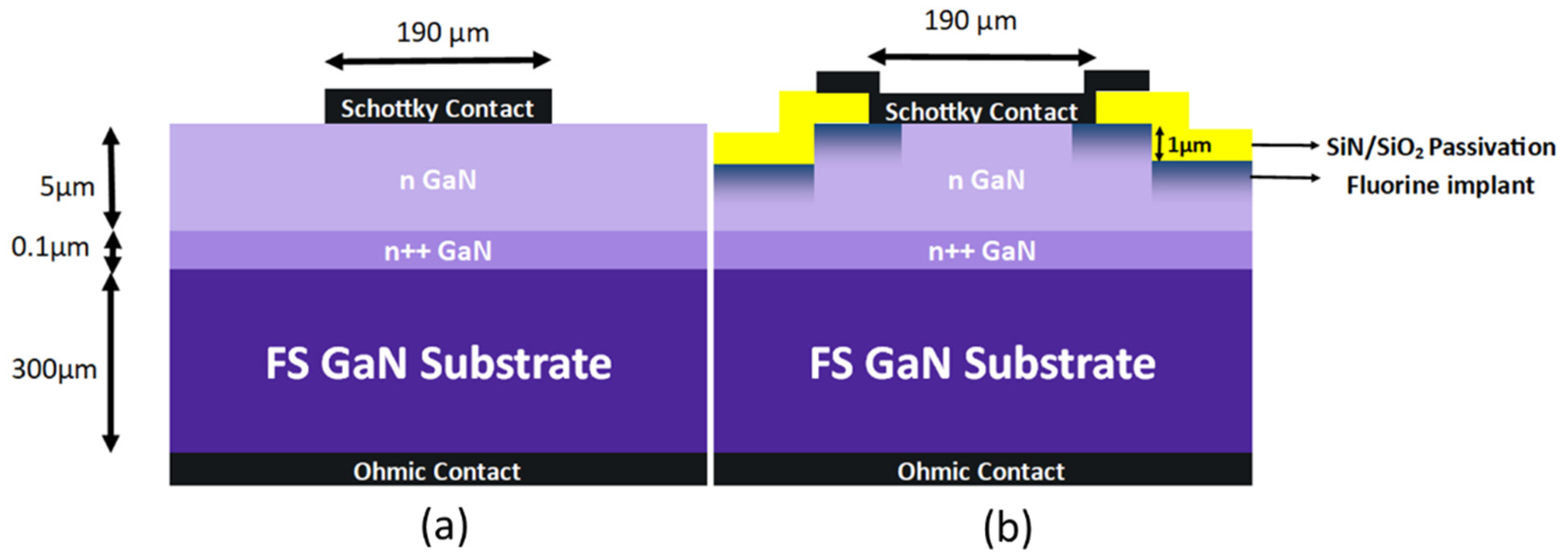
2. Materials and Methods

For this study, GaN layers were grown by metal-organic vapor-phase epitaxy (MOVPE) in a close-coupled showerhead reactor on a highly n+-doped (around 2 × 1018 cm−3), 2 inch diameter, 300 µm thick GaN free-standing substrate provided by Saint-Gobain Lumilog. A highly doped 0.1 µm buffer layer was also grown on top of the substrate before the epitaxy of the 5 µm, lightly doped drift layer (Nd-Na = 1~2 × 1016 cm−3), as illustrated in Figure 1. The quality of the crystal was characterized by X-ray diffraction (XRD) measurements. The full-width half-maximum (FWHM) of (002) symmetric and (302) asymmetric plane rocking curves (RCs) were 169 arc sec and 115 arc sec, respectively. The wafer was cleaved into six pieces, two of which were used for Schottky-barrier diode (SBD) fabrication. On one part, device fabrication started with 1 µm deep mesa isolation using ICP etching with Cl2 plasma chemistry, followed by multi-energy and multi-dose fluorine ion implantation to form the edge termination (implanted device). The implant dose and energy were taken from study [27]. Fluorine implantation has been widely used in GaN-based power devices to provide a negative fixed charge, which is effective in spreading the peak electric field away from the edge of the Schottky contact. Post-implantation, the wafer was annealed at 450 °C. A Ti/Al/Ni/Au metal stack was evaporated on the backside of the wafer to form an ohmic contact, and Pt/Au was used as the Schottky contact. The contacts were annealed simultaneously at 300 °C in a nitrogen environment for 5 min. A bilayer SiN/SiO2 was deposited as the passivation and was opened to deposit a Ti/Au field plate contact. For the non-implanted control diode, the same contact layers were deposited and annealed. The schematic cross-sections of the non-implanted and implanted diodes are represented in Figure 1a and Figure 1b, respectively.
Forward and reverse characterizations on the fabricated diodes were conducted using a Keithley 4200 parameter analyzer, and the temperature was varied from 25 °C to 125 °C, as shown in Figure 2a and Figure 2b, respectively. The analyzed devices had square geometry, with the Schottky contact side length being 190 µm. For the devices without implantation, as no edge termination was used, the measurement voltage was restricted to −50 V to prevent the device from undergoing destructive breakdown, due to electric field crowding at the Schottky contact edge. For the fluorine implanted devices, the measurements were conducted up to −200 V, which was the maximum voltage range of the equipment.

3. Results

3.1. Forward Bias

In the case of an ideal Schottky contact, the temperature (T)- and bias (V)-dependent current (I) can be expressed as [28]:
I = I s exp q V n k T 1 ,
I s = A A * T 2 e x p q B k T ,
A * = 4 π q m * k 2 h 3 ,
Here, I s is the saturation current density obtained by extrapolating a semi-log I-V curve to V = 0 V. A is the Schottky contact area, m* is the effective mass of an electron, A* is the effective Richardson constant (taken at 26.4 A cm−2 K−2 for m* = 0.2 from [29]), k is the Boltzmann constant, q is the elementary charge, h is the Planck constant, and B is the Schottky barrier height. The ideality factor, n, describes the dominant current transport mechanism, with a value close to unity indicating that the main mechanism is thermionic emission. When n is slightly larger than unity, it refers to a conduction mechanism that is composed of both thermionic emission and tunneling, while a large value of n indicates a tunneling-dominated conduction.
The extracted values of n at RT for both devices were 1.02 and 1.05, respectively, as shown in Figure 3. This suggests that the dominant conduction mechanism in forward bias is thermionic emission. The forward bias characteristics of both the implanted and non-implanted diodes exhibited different levels of current density, as can be observed from Figure 2a, due to the difference in the Schottky barrier heights, which were calculated at 0.76 eV and 0.96 eV (at RT) for the implanted and non-implanted diodes, respectively. The barrier height for the implanted device was 0.2 eV lower than that of the non-implanted one, which can be attributed to changes in the metal contact–GaN interface, due to multiple process steps, such as chemical cleaning and the annealing steps performed for the implanted device. Such steps can introduce surface states that can lead to inhomogeneous barrier height and B deviation from the Schottky–Mott model [28]:
B = M χ
In the above calculation of barrier height, A* was assumed to be constant at 26.4 A cm−2K−2. This calculation assumed an ideal case with a perfect barrier and crystal. However, in reality, this value depends considerably on the homogeneity of the Schottky interface and on crystal quality. Therefore, from the I-V-T measurement, the modified Richardson’s constant was extracted from the thermionic emission model, as given by [30]:
l n I S A T 2 = ln A * q b k T
The barrier heights extracted from the slope of Figure 4 were 0.69 eV and 0.83 eV for the implanted and non-implant diodes, respectively. These values were slightly lower than the previous extracted values, but there was a similar difference between the two samples. The experimental values of A* for the implanted and non-implanted diodes were found to be 2 A cm−2 K−2 and 0.23 A cm−2 K−2, respectively. This underestimation of Richardson’s constant from the ideal value could be explained by the presence of inhomogeneous distribution of the Schottky barrier and has been extensively studied before for Schottky–GaN contacts [31,32,33,34,35,36]. Due to the inhomogeneity in the barrier, the electrons at a higher temperature had sufficient energy to overcome a higher barrier, thus increasing the average barrier with the temperature, as can be observed from Figure 3. A comparative higher value of A* for the implanted device could indicate a larger effective area [37], due to the reduction in surface defects, interface roughness, or any other contamination, due to different cleaning and annealing steps involved in the fabrication.

3.2. Reverse Bias

Both the diodes had much higher leakage currents than those expected from the ideal thermionic equation. The physical origin of leakages can be either from the contact-limited processes, such as Schottky barrier lowering, direct tunneling through the contact, Fowler–Nordheim tunneling, and semiconductor bulk-limited conduction, such as PFE, VRH, SCLC, etc., or a combination of both contact- and-bulk related processes. A list of different mechanisms is presented in Table 1. In order to understand the leakage mechanism(s), the field and temperature dependences of the leakage currents were studied and simulated in Synopsys TCAD. As both the devices exhibited different forward barrier heights and leakage current densities, they were analyzed and simulated separately.

3.2.1. Non-Implanted Devices

For non-implanted diodes, the leakage current increased more rapidly than for implanted ones. The origin of this high leakage could be a phonon-assisted tunneling mechanism [26], as observed from the linear dependence in the ln(J) vs. E2 plot in Figure 5. According to this model, the current transport across the barrier was governed by the tunneling of electrons from the interface states [39]. Note that the electric field strength (E) was calculated using the formula:
E = 2 q ( N d N a ) ε r ε o ( V + V b i k T q ) ,
where V b i is the built-in voltage, N d   and N a are the donor and acceptor concentrations in the drift layer, respectively, V is the applied potential, ε r is the relative permittivity of GaN, and ε o is the permittivity of free space.
In order to confirm this, two dimensional TCAD simulations were performed (as the supplementary materials shown), with structural parameters the same as those of the fabricated devices, as mentioned in the previous section. The work function (WF) of the Schottky contact in the simulation was used as a fitting parameter to match the experimental forward I-V. We obtained a good fit, with a Schottky WF of 4.91 eV that gave a barrier height of 0.95 eV using Equation (4) (electron affinity χ = 3.96 eV for GaN at RT). This was in agreement with the extracted barrier height of 0.96 eV by I-V measurements. For simulating the reverse bias leakage through phonon-assisted tunneling, trap states were introduced at the Schottky interface, with trap energy, concentration, and thickness of the interface as the fitting parameters. Two tunneling paths were defined for electrons to tunnel from the metal to the trap state and for the subsequent tunneling to the conduction band [40]. An electron effective mass value of 0.2 m e was used. The electron–phonon-coupling Huang–Rhys factor was taken as 6.5, and the phonon energy h ω o was taken as 66 meV [41]. Thermionic emission and barrier lowering by image force were also included in the simulation. For a trap concentration of 2 × 1017 cm−3 and a trap location at 0.25 eV from the conduction band edge, a decent fit was obtained between the simulation and the experiment, as plotted in Figure 5b. The thickness of the interface layer was estimated to be 10 nm. This particular trap could be associated with nitrogen vacancies or point defects segregated around a dislocation [42,43,44,45]. Further investigation is required to fully understand the origin of this defect state.

3.2.2. Implanted Devices

The temperature and field dependence of the implanted devices suggested the presence of another mechanism apart from phonon-assisted tunneling, which could be related to the presence of defects in the 5 µm epitaxial GaN layer. Thermal activation energy E A was extracted at different voltages by linear fitting of the Arrhenius plot, according to the equation I e x p E A k T . The extracted E A v s . E 1 / 2 suggested Poole–Frenkel emission (PFE) as a possible conduction mechanism, which is the thermal excitation of deep states in the presence of an electric field. The field dependence of activation energy for PF is given by the relation:
E A = t β P F E 1 / 2 ,
β P F = q π ε 0 ε r ,
where t is the emission barrier height for the deep state, β P F is the Poole–Frenkel coefficient, ε r is the relative dielectric constant at high frequency, and E is the electric field. Two trap energies were extracted, with energy values of 0.75 eV and 1 eV below the conduction band, and β P F were equal to 1.8 × 10⁻⁴ eV·V−1/2·cm−1/2 and 5.5 × 10⁻⁴ eV·V−1/2·cm−1/2, respectively, as plotted in Figure 6a. The extracted β P F were in close agreement with previously reported values [19,21,46]. To reinforce this, TCAD simulations were performed by including bulk traps, with the PFE model activated in the GaN drift layer. Only a single trap energy was considered to simplify the simulation process, while the energy and concentration were used as the fitting parameters. A good fit was obtained between the simulation and the experimental leakages for a bulk trap of Ec—0.9 eV, with a trap concentration of 1 × 1015 cm−3, as plotted in Figure 6b.
The identified traps at 0.75 eV and 1 eV could be possibly related to G a 1 2 + , V G a N i and V G a N i 2 states [47], or dislocation-related defects [48]. However, additional experiments such as DLTS is required to confirm these observed traps.

4. Conclusions

In this work, we investigated both the forward and reverse characteristics of fluorine-implanted and non-implanted Schottky diodes in order to determine the conduction mechanisms. Both the devices were fabricated on different pieces of the same wafer, but they exhibited different forward and reverse characteristics. This clearly indicates that different fabrication steps, such as plasma etching, implantation, and passivation deposition, can alter the electrical characteristics of a Schottky–GaN interface significantly in both forward and reverse biases. The dominant conduction mechanism in the forward bias was found to be thermionic emission, with an ideality factor close to unity. The Schottky barrier heights were calculated at 0.76 eV and 0.96 eV (at RT) for the implanted and non-implanted diodes, respectively. The Richardson’s constant was extracted from the thermionic emission model, which revealed an underestimation of the Richardson’s constant from the ideal value, indicating the presence of inhomogeneous distributions of the Schottky barriers. In the reverse bias, two different mechanisms were identified and simulated through TCAD. For the non-implanted diodes, phonon-assisted tunneling through a trap located close to the M–S interface at 0.25 eV below the conduction band was identified as the source of the leakage. For the implanted diodes, Poole–Frenkel emissions from defects located deep in the bandgap appeared to be responsible for the observed leakage. A TCAD simulation successfully reproduced the experimental reverse I-V at different temperatures.

Supplementary Materials

The following supporting information can be downloaded at: https://www.mdpi.com/article/10.3390/en16145447/s1.

Author Contributions

Conceptualization, V.M., J.B., D.A., M.-R.I., H.H. and M.C.; formal analysis, V.M.; funding acquisition, J.B., M.C. and V.S.; investigation, V.M., J.B. and D.A.; methodology, V.M.; project administration, J.B., M.C. and V.S.; resources, M.-R.I. and H.H.; software, J.B. and M.-A.J.; supervision, J.B. and D.A.; validation, J.B., D.A. and M.C.; visualization, V.M.; writing—original draft, V.M.; writing—review and editing, J.B., D.A. and M.C. All authors have read and agreed to the published version of the manuscript.

Funding

This work is part of the VertiGaN project supported by the Labex GANEXT (ANR-11-LABX-0014).

Institutional Review Board Statement

Not applicable.

Informed Consent Statement

Not applicable.

Data Availability Statement

Data are contained within the article.

Acknowledgments

The authors would like to thank Yvon Cordier and his team from CNRS, CRHEA for developing the GaN-on-GaN epitaxy.

Conflicts of Interest

The authors declare no conflict of interest.

References

  1. Roccaforte, F.; Greco, G.; Fiorenza, P.; Iucolano, F. An overview of normally-off GaN-based high electron mobility transistors. Materials 2019, 12, 1599. [Google Scholar] [CrossRef] [Green Version]
  2. Le Royer, C.; Mohamad, B.; Biscarrat, J.; Vauche, L.; Escoffier, R.; Buckley, J.; Becu, S.; Riat, R.; Gillot, C.; Charles, M.; et al. Normally-OFF 650V GaN-on-Si MOSc-HEMT Transistor: Benefits of the Fully Recessed Gate Architecture. In Proceedings of the 2022 IEEE 34th International Symposium on Power Semiconductor Devices and ICs (ISPSD), Vancouver, BC, Canada, 22–25 May 2022; pp. 49–52. [Google Scholar] [CrossRef]
  3. Jaud, M.A.; Baines, Y.; Charles, M.; Morvan, E.; Scheiblin, P.; Torres, A.; Plissonnier, M.; Barbe, J.C. TCAD for gate stack optimization in pGaN Gate HEMT devices. In Proceedings of the 2017 International Conference on Simulation of Semiconductor Processes and Devices (SISPAD), Kamakura, Japan, 7–9 September 2017; pp. 113–116. [Google Scholar] [CrossRef]
  4. Hamady, S.; Morancho, F.; Beydoun, B.; Austin, P.; Gavelle, M. A new concept of enhanced-mode GaN HEMT using fluorine implantation in the GaN layer. In Proceedings of the 2013 15th European Conference on Power Electronics and Applications (EPE), Lille, France, 2–6 September 2013; pp. 1–6. [Google Scholar] [CrossRef]
  5. Meneghini, M.; Chowdhury, S.; Derluyn, J.; Medjdoub, F.; Ji, D.; Chun, J.; Kabouche, R.; De Santi, C.; Zanoni, E.; Meneghesso, G. GaN-Based Lateral and Vertical Devices; Springer: Cham, Switzerland, 2023; ISBN 9783030798277. [Google Scholar]
  6. Ozbek, A.M.; Baliga, B.J. Planar nearly ideal edge-termination technique for GaN devices. IEEE Electron Device Lett. 2011, 32, 300–302. [Google Scholar] [CrossRef]
  7. Liu, X.; Zou, P.; Wang, H.; Lin, Y.; Wu, J.; Chen, Z.; Wang, X.; Huang, S. Vertical GaN Schottky Barrier Diode with Record High Figure of Merit (1.1 GW/cm2) Fully Grown by Hydride Vapor Phase Epitaxy. IEEE Trans. Electron Devices 2023, 70, 3748–3753. [Google Scholar] [CrossRef]
  8. Liu, X.; Liu, Q.; Li, C.; Wang, J.; Yu, W.; Xu, K.; Ao, J.P. 1.2 kV GaN Schottky barrier diodes on free-standing GaN wafer using a CMOS-compatible contact material. Jpn J. Appl. Phys. 2017, 56, 26501. [Google Scholar] [CrossRef]
  9. Fukushima, H.; Usami, S.; Ogura, M.; Ando, Y.; Tanaka, A.; Deki, M.; Kushimoto, M.; Nitta, S.; Honda, Y.; Amano, H. Vertical GaN p-n diode with deeply etched mesa and the capability of avalanche breakdown. Appl. Phys. Express 2019, 12, 026502. [Google Scholar] [CrossRef]
  10. Hsu, J.W.P.; Manfra, M.J.; Lang, D.V.; Richter, S.; Chu, S.N.G.; Sergent, A.M.; Kleiman, R.N.; Pfeiffer, L.N.; Molnar, R.J. Inhomogeneous spatial distribution of reverse bias leakage in GaN Schottky diodes. Appl. Phys. Lett. 2001, 78, 1685–1687. [Google Scholar] [CrossRef] [Green Version]
  11. Phys, J.A. Effect of threading dislocation density on Schottky diode characteristics Effect of threading dislocation density on Ni / n -GaN Schottky diode. J. Appl. Phys. 2006, 100, 023709. [Google Scholar] [CrossRef] [Green Version]
  12. Sang, L.; Ren, B.; Sumiya, M.; Liao, M.; Koide, Y.; Tanaka, A.; Cho, Y.; Harada, Y.; Nabatame, T.; Sekiguchi, T.; et al. Initial leakage current paths in the vertical-type GaN-on-GaN Schottky barrier diodes. Appl. Phys. Lett. 2017, 111, 122102. [Google Scholar] [CrossRef]
  13. Yao, Y.; Sugawara, Y.; Yokoe, D.; Sato, K.; Ishikawa, Y.; Okada, N.; Tadatomo, K.; Sudo, M.; Kato, M.; Miyoshi, M.; et al. Correlation between structural properties and nonradiative recombination behaviors of threading dislocations in freestanding GaN substrates grown by hydride vapor phase epitaxy. CrystEngComm 2020, 22, 8299–8312. [Google Scholar] [CrossRef]
  14. Usami, S.; Ando, Y.; Tanaka, A.; Nagamatsu, K.; Deki, M.; Kushimoto, M.; Nitta, S.; Honda, Y.; Amano, H.; Sugawara, Y.; et al. Correlation between dislocations and leakage current of p-n diodes on a free-standing GaN substrate. Appl. Phys. Lett. 2018, 112, 182106. [Google Scholar] [CrossRef]
  15. Hamachi, T.; Tohei, T.; Hayashi, Y.; Imanishi, M.; Usami, S.; Mori, Y.; Sakai, A. Comprehensive analysis of current leakage at individual screw and mixed threading dislocations in freestanding GaN substrates. Sci. Rep. 2023, 13, 2436. [Google Scholar] [CrossRef] [PubMed]
  16. Structures, N. Leakage mechanism in GaN and AlGaN Schottky interfaces. Appl. Phys. Lett. 2006, 4884, 10–13. [Google Scholar] [CrossRef]
  17. Kotani, J.; Hashizume, T.; Hasegawa, H.; Kotani, J.; Hashizume, T.; Hasegawa, H. Analysis and control of excess leakage currents in nitride-based Schottky diodes based on thin surface barrier model. J. Vac. Sci. Technol. B Microelectron. Nanometer Struct. Process. Meas. Phenom. 2006, 22, 2179–2189. [Google Scholar] [CrossRef]
  18. Jin Ha, W.; Chhajed, S.; Jae Oh, S.; Hwang, S.; Kyu Kim, J.; Lee, J.H.; Kim, K.S. Analysis of the reverse leakage current in AlGaN/GaN Schottky barrier diodes treated with fluorine plasma. Appl. Phys. Lett. 2012, 100, 132104. [Google Scholar] [CrossRef] [Green Version]
  19. Peta, K.R.; Kim, M.D. Leakage current transport mechanism under reverse bias in Au/Ni/GaN Schottky barrier diode. Superlattices Microstruct. 2018, 113, 678–683. [Google Scholar] [CrossRef]
  20. Fu, K.; Zhou, J.; Deng, X.; Qi, X.; Smith, D.J.; Goodnick, S.M.; Zhao, Y.; Fu, H.; Huang, X.; Yang, T.H.; et al. Reverse Leakage Analysis for As-Grown and Regrown Vertical GaN-on-GaN Schottky Barrier Diodes. IEEE J. Electron Devices Soc. 2020, 8, 74–83. [Google Scholar] [CrossRef]
  21. Mukherjee, K.; De Santi, C.; Buffolo, M.; Borga, M.; You, S.; Geens, K.; Bakeroot, B.; Decoutere, S.; Gerosa, A.; Meneghesso, G.; et al. Understanding the leakage mechanisms and breakdown limits of vertical GaN-on-Si p+ n n diodes: The road to reliable vertical MOSFETs. Micromachines 2021, 12, 445. [Google Scholar] [CrossRef] [PubMed]
  22. Chen, J.; Liu, Z.; Wang, H.; Song, X.; Bian, Z.; Duan, X.; Zhao, S.; Ning, J.; Zhang, J.; Hao, Y. Determination of the leakage current transport mechanisms in quasi-vertical GaN-on-Si Schottky barrier diodes (SBDs) at low and high reverse biases and varied temperatures. Appl. Phys. Express 2021, 14, 10. [Google Scholar] [CrossRef]
  23. Diodes, G.; Li, S.; Ercan, B.; Ren, C.; Ikeda, H. A Study on the Impact of Dislocation Density on Leakage Current in Vertical. IEEE Trans. Electron Devices 2022, 69, 4206–4211. [Google Scholar]
  24. Zhang, Y.; Wong, H.Y.; Sun, M.; Joglekar, S.; Yu, L.; Braga, N.A.; Mickevicius, R.V.; Palacios, T. Design space and origin of off-state leakage in GaN vertical power diodes. In Proceedings of the Technical Digest—International Electron Devices Meeting, IEDM, Washington, DC, USA, 7–9 December 2015; Volume 2016, pp. 35.1.1–35.1.4. [Google Scholar]
  25. Guo, X.; Zhong, Y.; Chen, X.; Zhou, Y.; Su, S.; Yan, S.; Liu, J.; Sun, X.; Sun, Q.; Yang, H. Reverse leakage and breakdown mechanisms of vertical GaN-on-Si Schottky barrier diodes with and without implanted termination. Appl. Phys. Lett. 2021, 118, 243501. [Google Scholar] [CrossRef]
  26. Pipinys, P.; Lapeika, V. Analysis of reverse-bias leakage current mechanisms in metal/GaN schottky diodes. Adv. Condens. Matter Phys. 2010, 2010, 526929. [Google Scholar] [CrossRef] [Green Version]
  27. Han, S.; Yang, S.; Sheng, K. Fluorine-implanted termination for vertical GaN schottky rectifier with high blocking voltage and low forward voltage drop. IEEE Electron Device Lett. 2019, 40, 1040–1043. [Google Scholar] [CrossRef]
  28. Rhoderick, P.E.H.; Sc, M.; Ph, C.; Eng, P.F. Metal-Semiconductor Contacts; Clarendon Press: Oxford, UK, 1988; pp. 1–14. [Google Scholar]
  29. Knap, W.; Alause, H.; Bluet, J.M.; Camassel, J.; Young, J.; Asif Khan, M.; Chen, Q.; Huant, S.; Shur, M. The cyclotron resonance effective mass of two-dimensional electrons confined at the GaN/AlGaN interface. Solid State Commun. 1996, 99, 195–199. [Google Scholar] [CrossRef]
  30. Werner, J.H.; Güttler, H.H. Barrier inhomogeneities at Schottky contacts. J. Appl. Phys. 1991, 69, 1522–1533. [Google Scholar] [CrossRef]
  31. Iucolano, F.; Roccaforte, F.; Giannazzo, F.; Raineri, V. Barrier inhomogeneity and electrical properties of PtGaN Schottky contacts. J. Appl. Phys. 2007, 102, 113701. [Google Scholar] [CrossRef]
  32. Li, L.; Pu, T.; Li, X.; Ao, J.P. Effect of Anode Material on the Sensitivity of GaN Schottky Barrier Diode Temperature Sensor. IEEE Sens. J. 2022, 22, 1933–1938. [Google Scholar] [CrossRef]
  33. Mamor, M. Interface gap states and Schottky barrier inhomogeneity at metal/n-type GaN Schottky contacts. J. Phys. Condens. Matter 2009, 21, 335802. [Google Scholar] [CrossRef] [PubMed]
  34. Rajagopal Reddy, V.; Janardhanam, V.; Leem, C.H.; Choi, C.J. Electrical properties and the double Gaussian distribution of inhomogeneous barrier heights in Se/n-GaN Schottky barrier diode. Superlattices Microstruct. 2014, 67, 242–255. [Google Scholar] [CrossRef]
  35. Roccaforte, F.; Giannazzo, F.; Alberti, A.; Spera, M.; Cannas, M.; Cora, I.; Pécz, B.; Iucolano, F.; Greco, G. Barrier inhomogeneity in vertical Schottky diodes on free standing gallium nitride. Mater. Sci. Semicond. Process. 2019, 94, 164–170. [Google Scholar] [CrossRef]
  36. Greco, G.; Fiorenza, P.; Schilirò, E.; Bongiorno, C.; Di Franco, S.; Coulon, P.M.; Frayssinet, E.; Bartoli, F.; Giannazzo, F.; Alquier, D.; et al. Current transport in Ni Schottky barrier on GaN epilayer grown on free standing substrates. Microelectron. Eng. 2023, 276, 112009. [Google Scholar] [CrossRef]
  37. Roccaforte, F.; La Via, F.; Raineri, V.; Pierobon, R.; Zanoni, E. Richardson’s constant in inhomogeneous silicon carbide Schottky contacts. J. Appl. Phys. 2003, 93, 9137–9144. [Google Scholar] [CrossRef]
  38. Pipinys, P.; Lapeika, V. Temperature dependence of reverse-bias leakage current in GaN Schottky diodes as a consequence of phonon-assisted tunneling. J. Appl. Phys. 2006, 99, 093709. [Google Scholar] [CrossRef]
  39. Pipinys, P.; Pipiniene, A.; Rimeika, A. Phonon-assisted tunneling in reverse biased Schottky diodes. J. Appl. Phys. 1999, 86, 6875–6878. [Google Scholar] [CrossRef]
  40. Kampen, C.; Burenkov, A.; Lorenz, J. Challenges in TCAD simulations of tunneling field effect transistors. In Proceedings of the 2011 Proceedings of the European Solid-State Device Research Conference (ESSDERC), Helsinki, Finland, 12–16 September 2011; pp. 139–142. [Google Scholar] [CrossRef]
  41. Racko, J.; Pecháček, J.; Mikolášek, M.; Benko, P.; Grmanová, A.; Harmatha, L.; Breza, J. Trap-Assisted Tunneling in the Schottky Barrier. Radioengineering 2013, 22, 240–244. [Google Scholar]
  42. Koné, S.; Cayrel, F.; Yvon, A.; Collard, E.; Alquier, D. DLTS analysis of high resistive edge termination technique-induced defects in GaN-based Schottky barrier diodes. Phys. Status Solidi Appl. Mater. Sci. 2016, 213, 2364–2370. [Google Scholar] [CrossRef]
  43. Auret, F.D.; Goodman, S.A.; Koschnick, F.K.; Spaeth, J.M.; Beaumont, B.; Gibart, P. Sputter deposition-induced electron traps in epitaxially grown n-GaN. Appl. Phys. Lett. 1999, 74, 2173–2175. [Google Scholar] [CrossRef]
  44. Choi, K.J.; Jang, H.W.; Lee, J.L. Observation of inductively coupled-plasma-induced damage on n-type GaN using deep-level transient spectroscopy. Appl. Phys. Lett. 2003, 82, 1233–1235. [Google Scholar] [CrossRef]
  45. Ferrandis, P.; Charles, M.; Baines, Y.; Buckley, J.; Garnier, G.; Gillot, C.; Reimbold, G. Ion-assisted gate recess process induced damage in GaN channel of AlGaN/GaN Schottky barrier diodes studied by deep level transient spectroscopy. Jpn. J. Appl. Phys. 2017, 56, 04CG01. [Google Scholar] [CrossRef] [Green Version]
  46. Kuksenkov, D.V.; Temkin, H.; Osinsky, A.; Gaska, R.; Khan, M.A. Origin of conductivity and low-frequency noise in reverse-biased GaN p-n junction. Appl. Phys. Lett. 1998, 72, 1365–1367. [Google Scholar] [CrossRef]
  47. Auret, F.D.; Goodman, S.A.; Koschnick, F.K.; Spaeth, J.M.; Beaumont, B.; Gibart, P. Electrical characterization of two deep electron traps introduced in epitaxially grown n-GaN during He-ion irradiation. Appl. Phys. Lett. 1998, 73, 3745–3747. [Google Scholar] [CrossRef]
  48. Tokuda, Y.; Matsuoka, Y.; Ueda, H.; Ishiguro, O.; Soejima, N.; Kachi, T. DLTS study of n-type GaN grown by MOCVD on GaN substrates. Superlattices Microstruct. 2006, 40, 268–273. [Google Scholar] [CrossRef]
Figure 1. (a) Non-implanted diode; (b) implanted diode.
Energies 16 05447 g001
Figure 2. Temperature-dependent characterizations of (a) forward biases and (b) reverse biases of implanted (dashed line) and non-implanted (solid line) devices.
Energies 16 05447 g002
Figure 3. Ideality factor and barrier height extracted from the I-V measurements in the temperature range of 25 °C to 125 °C.
Energies 16 05447 g003
Figure 4. Richardson’s plot for implanted and non-implanted devices.
Energies 16 05447 g004
Figure 5. (a) Reverse ln(J) vs. E2 characteristics at different temperatures for the non-implanted diode. (b) TCAD fitting with the phonon-assisted tunneling model.
Energies 16 05447 g005
Figure 6. (a) Linear fitting E A v s . E 1 / 2 for extracting the PFE parameters for the implanted diode. (b) TCAD fitting of the reverse current density at different temperatures.
Energies 16 05447 g006
Table 1. Summary of different leakage mechanisms.
MechanismExpressionReference
Poole–Frenkel emission J P F = C E e x p q ( t q E / π ε r ε o ) k T   [18,19,21]
Variable-range hopping J V R H = J ( 0 ) e x p C q E a 2 k T T 0 T 1 4 [21,25]
Phonon-assisted tunneling J P h A T e x p E 2 E c 2 [26,38]
Space-charge-limited J S C L C V 2 [25]
Trap-assisted tunneling J T A T e x p 4 2 q m * t 3 / 2 3 ħ E [12]
Disclaimer/Publisher’s Note: The statements, opinions and data contained in all publications are solely those of the individual author(s) and contributor(s) and not of MDPI and/or the editor(s). MDPI and/or the editor(s) disclaim responsibility for any injury to people or property resulting from any ideas, methods, instructions or products referred to in the content.

