Article

Variable Amplitude Gate Voltage Synchronous Drive Technique for Improving Dynamic Current Balancing in Paralleled IGBTs

1
Electric Power Research Institute, Guangdong Power Grid Company, Ltd., Guangzhou 510030, China
2
School of Electrical Engineering, China University of Mining and Technology, Xuzhou 221116, China
*
Author to whom correspondence should be addressed.
Energies 2023, 16(14), 5306; https://doi.org/10.3390/en16145306
Submission received: 14 June 2023 / Revised: 3 July 2023 / Accepted: 6 July 2023 / Published: 11 July 2023

Abstract

:
The problem of current sharing imbalance in the parallel connection of IGBT multi-modules affects the wide-scale application of parallel IGBT. The current imbalance problem in the dynamic process is mainly caused by the difference in control loop parameters. In parallel IGBT applications, current sharing is a critical concern. Objective differences in IGBT module and driver circuit parameters, as well as incomplete symmetry in the power circuit, lead to inconsistent parasitic parameters, resulting in both static and dynamic current-sharing issues. Static current sharing refers to the uneven distribution of load current under static operating conditions, while dynamic current sharing refers to the imbalance in current distribution among parallel IGBT modules during turn-on and turn-off processes. This is mainly influenced by the synchronization of turn-on and turn-off timings and the consistency of collector current change rates during these processes. The difference in characteristic parameters of IGBT modules is an important factor leading to the difference in control loop parameters, which has a profound impact on the dynamic current-sharing characteristics of IGBT parallel applications. In the case where the device parameters cannot be changed, some drive compensation controls can compensate for the influence of device differences on dynamic current sharing. Accurate identification of the characteristic parameters of the IGBT module is the key to this method. This paper mainly studies a synchronous variable-amplitude drive scheme and studies the influence of parameters such as synthetic gate resistance, gate-emitter capacitance, and on-off gate threshold voltage on the dynamic current-sharing characteristics. The correlation characteristics of the characteristic parameters of the IGBT device body are studied, and the characteristic model of each parameter and the influencing variable is constructed. The parallel working model of PSpice devices is established, and the influence of different characteristic parameters on the current-sharing characteristics is evaluated, and its sensitivity is summarized through simulation analysis. Through the 1700 V/300 A IGBT parallel switch characteristic experiment, the current sharing effectiveness of the synchronous variable amplitude driving method is verified. Finally, the effects of different gate control voltages and different action times on the dynamic current-sharing characteristics are summarized.

1. Introduction

Due to the reliable hardware structure, simple control system, and low overall system cost, paralleling IGBT modules is an effective way to increase the transmission capacity of the converter system in high-voltage and large-capacity converter applications such as traction drive, wind power generation, and smart grid. When multiple IGBT modules are used in parallel, the power loop structure, drive control capability, IGBT device characteristic parameters, and junction temperature variation distribution may cause static and dynamic uneven current problems of IGBT. Optimizing the control structure and the power loop design can minimize the influence of different branch parameters on the current sharing [1,2,3,4]. The symmetrical design of the power loop is adopted to optimize the layout’s physical size and mounting structure [5]. The power loop’s equivalent circuit impedance formation material, form, and current path are considered for impedance matching design in [6,7,8]. In addition, the low-inductance connection technology, the optimization of the electromechanical connection, and device layout design [9] are adopted, which can effectively reduce the influence of power loop impedance differences and parasitic parameters on current inhomogeneity. The current density distribution of parallel branches caused by the difference in physical structure and stray impedance when the same circuit has different layouts and optimizes the design of the parallel power circuit is studied in [10]. The difference in control loop parameters is the key to affecting the dynamic current-sharing characteristics of IGBTs in parallel. In practical applications, most control loops are symmetrically designed to synchronize the gate pulses to reduce the influence [11,12,13]. Using a universal grid design, the collector current balance is adjusted by controlling the grid resistance and parasitic inductance values to minimize delay and voltage level issues.
Furthermore, temperature is an important parameter affecting and relating to static current sharing. To ensure the consistency of characteristic parameters, it is necessary to realize parallel current sharing [14,15]. Consistency requirements include the characteristic curve VCE(sat)-iC, the batch of modules with a positive temperature coefficient, and the same VGE(th) and temperature Tj. The higher the temperature, the higher the saturation. The larger the voltage drop, the more suitable for a parallel connection. In the literature [16], an asynchronous drive method is proposed to adjust the consistency of the opening and closing moments of each branch.
Due to the inherent differences in the characteristic parameters of the power devices in each parallel branch and the objective constraints of the design of the drive signal branch, there are certain differences in the dynamic current-sharing characteristics. Using a fully synchronous driving voltage to control the opening and closing of parallel IGBTs cannot achieve better dynamic current sharing [17]. By analyzing the relationship between voltage and current in the dynamic process, one branch is selected as the reference branch, and a driving voltage with a set amplitude is applied for some time during the current change stage of the other branch, so that the current slope of the controlled branch changes, to achieve the purpose of equalization. Reduce or even offset the above effects as much as possible.
This paper proposes a synchronous variable-amplitude current-sharing method and a current-sharing index to evaluate the current distribution. First, the four characteristic parameters of the IGBT module device body are studied [18,19,20], and the influencing variables of the characteristic parameters are analyzed. Then, the mathematical expression and physical model of the characteristic parameters are constructed, and the compensation value of the synchronous variable amplitude drive is deduced and calculated. Through the simulation analysis and experimental test, the effectiveness of the synchronous variable-amplitude driving method is verified. Finally, through parameter extraction, the characteristic parameters of the IGBT module with two modules connected in parallel are obtained, and the influence of different gate control voltages and different action times on the dynamic current-sharing characteristics is verified.

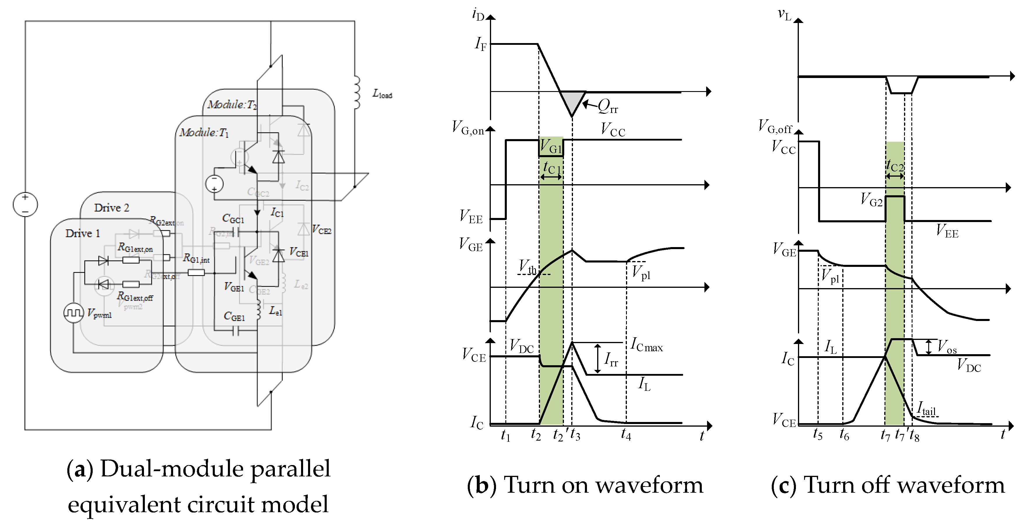
2. Modeling and Analysis of the Method of Synchronous Variable-Amplitude Drive of IGBTs in Parallel for Current Sharing Control

Figure 1 shows the circuit diagram of the parallel IGBT application circuit diagram including characteristic parameters affecting current sharing. The separate drive circuit and control loop correspond to the individual IGBT module. In the figure, the power loop is symmetrical and centralized. The drive and control loops are independent.
Among them, tdelay is the signal transmission delay time; VG,on is the gate turn-on voltage; VG,off is the gate turn-off voltage; RG,on is the gate turn-on resistance; RG,off is the gate turn-off resistance; RG,int is the gate module internal resistance; Tj is the junction temperature; Le is the module emitter inductance; CGC is the gate collector capacitance; CGE is the gate emitter capacitance; LG is the gate inductance; LC is the collector inductance; LE is the emission pole inductance; RC is the collector resistance; RE is the emitter resistance.
The driving principle of the synchronous variable-amplitude driving method is shown in Figure 2. For the case of ordinary synchronous pulse driving, it is shown in Figure 2a, assuming that the power loop parameters of IGBT module 1 and module 2 are completely consistent. Under the action of Vcontrol_2, due to the differences in the characteristic parameters of the drive circuit such as gate resistance, gate threshold voltage, and input capacitance, the variation trends of the gate voltage VGEx and collector current iCx of modules 1 and 2 are different in the dynamic process. The main performance is the dynamic uneven current caused by the asynchrony of the collector current at the turn-on and turn-off moments and the difference in rising and falling rates. As shown in Figure 2b, the synchronous variable-amplitude driving method introduces the calculated gate control voltage into the IGBT module 1 driving circuit to improve the synchronization of the two modules at the time of turning on and off, thereby improving the dynamic current sharing.

2.1. Analysis of the IGBT Operation Process with Synchronous Variable-Amplitude Driving Method

For better description and illustration, this paper analyzes the case of two IGBT modules connected in parallel, as shown in Figure 3a. Figure 3b and Figure 3c represent the waveforms of the turn-on and turn-off processes. The gate loop parameters can significantly impact the switching process. Meanwhile, the influence of gate loop parameters on IGBT operation concentrates on the turn-on delay, the collector current rise, the turn-off delay, and the collector voltage rise.

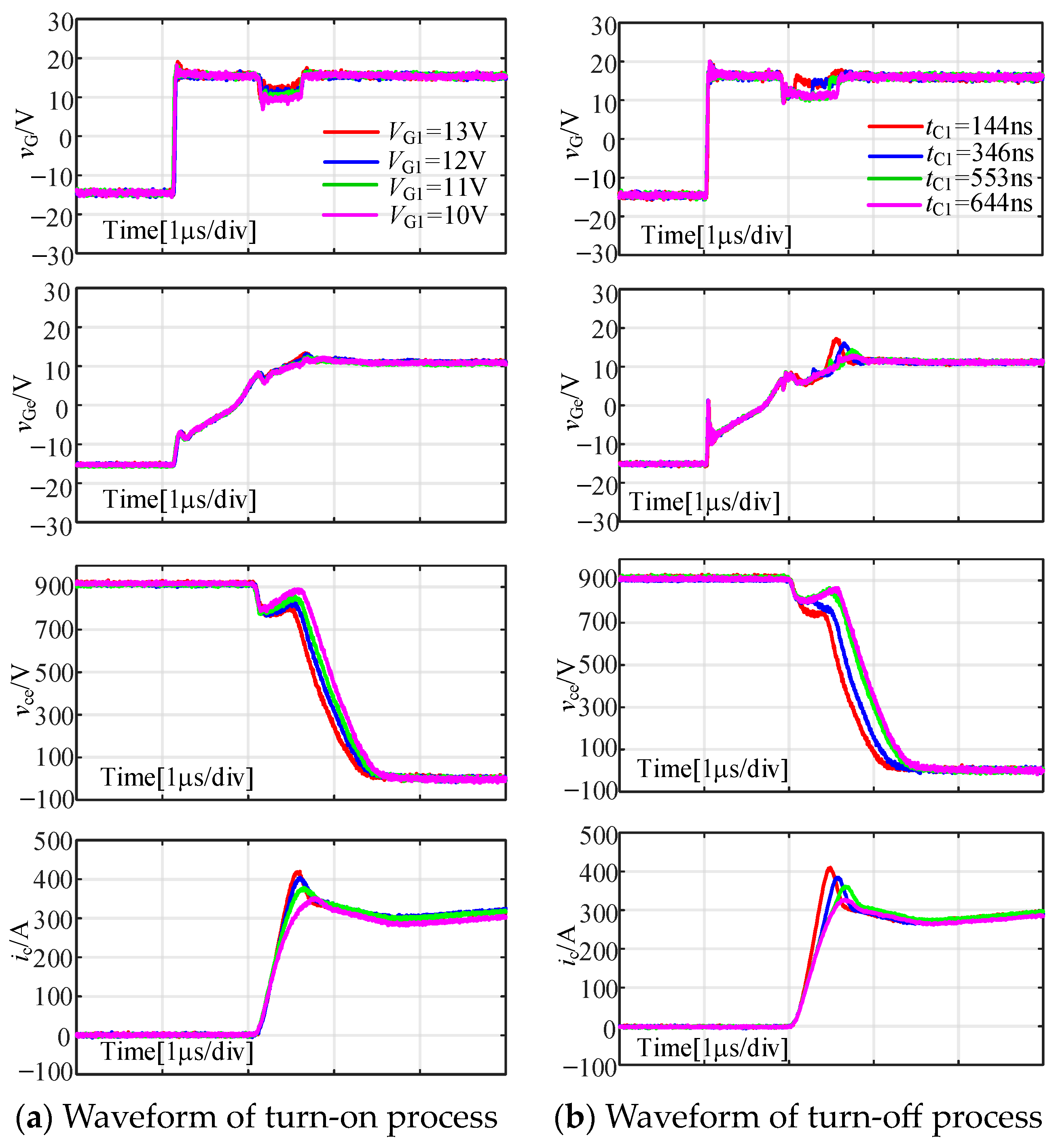
2.1.1. Turn-On Delay

The driving circuit applies a forward voltage VGx,on, representing the parallel branch number, defined as 1, 2 in this paper). It charges the input capacitor Ciesx through the gate resistor RGx,on. Hence, the voltage across Ciesx gradually rises. The input capacitor Ciesx is the gate-emitter capacitor CGEx. The IGBT gate voltage VGEx rises to the turn-on threshold voltage VGE(th)x.
At t1~t2 stage, the MOS channel has not yet been formed, the collector current iCx is 0, and the collector-emitter voltage VCE is the same as the bus voltage. The circuit formula is as follows:
V Gx , on = R Gx , on C iesx d v GE x d t + v GE x V GE x ( 0 ) = V G x , off I C x = 0
where VGx,on is the turn-on drive voltage used by the drive control circuit, and VGx,off is the turn-off drive voltage used by the drive control circuit. The turn-on gate resistance RGx,on is the sum of the external drive resistance and the built-in resistance of the IGBT module given in the device manual for actual use.
The turn-on delay stage expression of the gate voltage VGE is obtained by solving the resistor-capacitance circuit formula, and the turn-on delay time td(on)x is obtained by substituting VGex = VGE(th)x, as shown in Formula (2):
t d ( on ) x = C iesx R Gx , o n ln V G , on V GE ( th ) x V Gx , on V Gx , off

2.1.2. Collector Current Rise

When the gate voltage exceeds the turn-on threshold voltage, the collector current iCx rises rapidly. The anti-parallel diode goes to the off-state. At the same time, the VCE begins to drop until iCx rises to the load current. At this stage, the gate circuit is shown in Formula (3). The expression of the collector current is shown in Formula (4):
V Gx , on = v GEx + R Gx , on C iesx d v GEx d t + L Ex d i Cx d t
i Cx = 0 v GEx V GE ( th ) x , V CE < 0 K ( v GEx V GE ( th ) x ) 1 2 V CE 2 v GEx > V GE ( th ) x , V CE v GEx V GE ( th ) x K 2 ( v GEx V GE ( th ) x ) 2 V CE > v GEx V GE ( th ) x > 0
where LEx is the auxiliary emitter inductance, and K is the equivalent transconductance. gfsx is the forward transfer rate and can be expressed as:
g f s x = d i Cx d v GE x = K v GE x V GE ( th ) x
The above Formulas (3)–(5) can be derived to calculate the collector current rise rate, as shown in Formula (6):
d i C x d t V GE x V GE ( th ) x R G x , on C ies x / g fsx + L Ex
The current overshoot caused by the reverse recovery of the diode after the current rising stage reaches the rated value of the load current can be expressed as Formula (7), as one of the parameters for judging the dynamic characteristics of the module.
I rrx = 2 Q rrx d I Cx ( on ) / d t ( S + 1 ) = 2 Q rrx ( S + 1 ) V CC ( I L g fsx + V GE ( th ) x ) R Gx , on C iesx g fsx + L Ex
The equivalent principle of the current rise rate under the action of the drive control voltage is shown in Figure 4. The idea of average equivalent is adopted in the whole current change process [21], and the current rise rate before and after the drive control is added is replaced by the equivalent current rise rate. The analysis of current unbalance is calculated by the equivalent current rise rate.
In Figure 4, t3 represents the moment when the collector current iC rises to the maximum value iCmax, the gate control voltage in the initial state is VCC, when the gate drive control voltage introduced in the t2-t2G stage is VG1, the corresponding current slope is diC/dt2, the action time of introducing VG1 is tC1; after the action time ends, the gate drive voltage returns to VCC in the t2G~t3 stage, and the corresponding current slope is diC/dt3, and diC/dt2 and diC/dt3, etc. The effect is the current slope diC/dt(eq1), which can be equivalently expressed by diC/dt2 and diC/dt3 as:
d i C d t 2 t C 1 + d i C d t 3 ( t 3 t 2 t C 1 ) = d i C d t eq 1 ( t 3 t 2 ) = I L
Substituting Formula (8) into Formula (6), the relationship between the equivalent current slope diC/dt(eq1) and characteristic parameters can be obtained as:
d i C d t eq 1 = d i C d t 3 I L / [ I L + ( d i C d t 3 d i C d t 2 ) t C 1 ] = V CC ( I L g fs + V GE ( th ) ) ( R G , on C ies g fs + L E ) + ( V CC V G 1 ) t C 1 I L
From the Formula (9), it can be known that the gate control voltage VG1 and the action time tC1 have a control effect on the equivalent current slope diC/dt(eq1), and the action time tC1 ranges from 0 to t3-t2. The duration of this stage is divided into the current rising from 0 to the load current, and the current rising from the load current to the maximum current overshoot under the action of the anti-parallel diode. The duration of the ramp-up to load current phase can be expressed as:
t 2 - 2 G = I L d i C / d t eq 1 = I L R G , on C ies g fs + L E + ( V CC V G 1 ) t C 1 V CC I L g fs + V GE ( th )
The equivalent current overshoot Irr can be obtained by solving Formulas (7) and (9):
I rr = 2 Q rr d i C / d t eq 1 ( S + 1 ) = 2 Q rr ( S + 1 ) V CC ( I L g fs + V GE ( th ) ) ( R G , on C ies g fs + L E ) + ( V CC V G 1 ) t C 1 I L
The reverse recovery time factor usually takes S = 1, so the duration of the t2G~t3 stage from the load current rise to the maximum current overshoot is:
t 2 G - 3 = Q rr ( R G , on C ies g fs + L E ) + ( V CC V G 1 ) t C 1 I L V CC ( I L g fs + V GE ( th ) )
From Formulas (11) and (12), we can see that t2–3 is negatively correlated with VG1 and positively correlated with tC1, and Irr is positively correlated with VG1 and negatively correlated with tC1.
In the case of parallel connection of IGBT modules T1 and T2, the current rise rate of module T2 is adjusted with module T1 as a reference, that is, diC1/dt = diC2/dteq1, so after compensation, the current rise rate compensation value at this stage is:
ε on = V CC V G 1 t C 1        = I L V CC I L g fs 2 + V GE ( th ) 2 V CC I L g fs 1 + V GE ( th ) 1 R G 1 , on C ies 1 g fs 1 + L E 1 R G 2 , on C ies 2 g fs 2 + L E 2

2.1.3. Turn-Off Delay

The turn-off process is the capacitor discharge process, which is the opposite of the turn-on process. Before the shutdown signal arrives, the IGBT is in the on-state [22,23,24]. And the gate voltage is VGEx = VGx,on. Hence, the collector voltage is the on-state saturation voltage drop VCE(sat). After the shutdown signal arrives, the input capacitor Ciesx begins to discharge, and the gate voltage drops until it reaches VGE(pl)x. Similar to the turn-on delay stage, the turn-off delay time of this stage is shown in the Formula (14):
t d ( off ) x = C iesx R Gx , off ln V GE ( pl ) x V Gx , off V Gx , on V Gx , off

2.1.4. Collector Voltage Rise

When the gate voltage drops to the Miller plateau, the gate current iGx passes almost only through the gate collector capacitor CGCx, and the collector voltage rises. The gate voltage is maintained near the Miller plateau voltage VGE(pl)x. The rising rate of the collector voltage at this time is shown in Formula (15):
d v CEx d t = i Gx C GCx = V GE ( pl ) x V Gx , off R Gx , off C GCx

2.1.5. Collector Current Drop Stage

After VCE reaches VDC, the collector current starts to drop from the load current. The current drop rate in this stage can be expressed as:
d i Cx d t = V Gx , off ( I L g fsx + V GE ( th ) x ) R Gx , off C iesx g fsx + L Ex
The collector voltage process generated at this stage is mainly due to the induced voltage generated by the current change on the parasitic inductance of the power loop, and the voltage overshoot Vos can be expressed as:
V os = L p d i c ( off ) d t = L p ( I L g m + V th ) V EE R C ies g m + L E
Similarly, according to the current equivalent principle of the equivalent schematic diagram of the turn-off current drop rate in Figure 5, where the influence of the tail current is ignored, it is considered that the current is zero at time t8, and the equivalent current slope diC/dt of the turn-off process at this time can be expressed as:
d i c d t ( eq 2 ) = V EE ( V GE ( th ) + I L g fs ) ( R G , off C ies g fs + L E ) + ( V EE V G 2 ) t C 2 I L
It can be seen from the Formula (18) that the gate control voltage VG2 and the action time tC2 have a control effect on the equivalent current slope diC/dt(eq2) in the current falling stage, ignoring the influence of the tail current, and the value range of the action time tC2 is 0~t8-t7.
Solving the Formulas (17) and (18), the equivalent voltage overshoot Vos of the turn-off process can be obtained as:
V os = L P d i C d t ( eq 2 ) = L P ( V GE ( th ) + I L g fs ) V EE ( R G , off C ies g fs + L E ) + ( V EE V G 2 ) t C 2 I L
The duration of this phase can be expressed as:
t 7 8 = I L I tail d i c / d t eq 2 = ( I L I tail ) ( R G , off C ies g fs + L E ) + ( V EE V G 2 ) t C 2 I L ( V GE ( th ) + I L g fs ) V EE
From the Formulas (19) and (20), we can see that the voltage overshoot Vos is negatively correlated with VG2 and positively correlated with tC2; t7–8 is negatively correlated with VG2 and positively correlated with tC2.
In the case of parallel connection of IGBT modules T1 and T2, module T1 is used as a reference to adjust the current rise rate of module T2, that is, diC1/dt = diC2/dteq2. Therefore, after compensation, the compensation value of the current drop rate at this stage is:
ε off = V EE V G 2 t C 2        = I L V EE I L g fs 2 + V GE ( th ) 2 V EE I L g fs 1 + V GE ( th ) 1 R G 1 , off C ies 1 g fs 1 + L E 1 R G 2 , off C ies 2 g fs 2 + L E 2
Through the analysis of the turn-on and turn-off process, it can be seen that the characteristic parameters of the drive circuit, including the gate-emitter capacitance CGE, the gate-collector capacitance CGC, the gate resistance RG and the turn-on threshold voltage VGE(th), will affect the parameters of each parallel branch. Current dynamic characteristics in the process of IGBT switching.

2.2. PSpice Modeling with the IGBT Parameters

The synchronous variable-amplitude driving model is constructed using PSpice for two parallel IGBTs. Meanwhile, the influence of the gate loop characteristic parameters on the current sharing is compared and analyzed. ΔIc is the collector current difference between T1 and T2 modules, expressed as ΔIc = Ic1Ic2. This value can represent the degree of current balance in the switching process. The formula follows t 0 t 1 Δ I C = t 0 t 1 I C 1 I C 2 d t (t0~t1 is the opening process) and t 2 t 3 Δ I C = t 2 t 3 I C 1 I C 2 d t (t2~t3 is the shutdown process). The current difference and current integral can be used as the evaluation index of current balance. At the same time, the degree of current imbalance can be expressed as:
δ = I C max I C min I C max + I C min
Figure 6a shows the current difference curve and integral curve when the relative difference of the gate-emitter capacitance of the T1 and T2 modules is different, reflecting the current difference of the two branches under this working condition. It can be seen from the figure that the gate-emitter capacitance error has a greater impact on the turn-on process; the greater the relative value of the gate-emitter capacitance difference, the smaller the current rise rate, and the more unbalanced the current distribution in the dynamic process. Figure 6b shows the influence of the relative difference of the gate-collector capacitance parameters on the turn-on and turn-off processes. It can be seen that the gate-emitter capacitance error has a more obvious impact on the turn-on process, the greater the relative value of the gate-emitter capacitance parameter difference, the smaller the current rise rate, and the more unbalanced the current distribution in the dynamic process. Figure 6c shows the influence of the relative difference of gate resistance parameters on the turn-on and turn-off processes. It can be seen that the larger the relative value of the gate resistance difference, the smaller the current rise rate, and the more unbalanced the current distribution in the dynamic process, and the impact on the turn-off process is more obvious than that in the turn-on process. Figure 6d shows the influence of the relative difference of the conduction threshold voltage parameter on the turn-on and turn-off processes. The larger the relative value of the conduction threshold voltage parameter difference, the smaller the current rise rate, and the more unbalanced the dynamic current distribution.
Combining the data comparison of the device manual and the simulation test parameters of multiple working conditions, considering the change of a single parameter itself, regardless of the simultaneous change of different parameters, the characteristic parameters and influencing factor change curves of the IGBT device are fitted, as shown in Figure 7. The figure shows the relationship between the degree of difference of different parameters and the degree of current imbalance. It can be seen that when the relative degree of difference is the same, the gate resistance has a greater impact on the turn-on and turn-off processes.
Through the simulation analysis of the synchronous variable-amplitude driving method in PSpice, its control effect on the turn-on and turn-off process is verified. If the gate on-resistance difference of the two branches is 3.0%, compare the synchronous variable-amplitude drive method before and after compensation, as shown in Figure 8, in which (a) is the current state without synchronous variable-amplitude drive control. The current unbalance degree is 6.62%. (b) Add synchronous variable-amplitude drive control to module 1. At this time, the current unbalance degree is 0.52%. Similarly, (c) add synchronous variable-amplitude drive control to module 2. At this time, the current unbalance degree is 0.74%. It can be seen that the synchronous variable-amplitude control is effective in the opening process.
If there is a gate turn-off resistance difference of 3.0% in the two branches, compare the synchronous variable-amplitude drive method before and after compensation, as shown in Figure 9a, which is the current state without adding synchronous variable-amplitude drive control. The unbalance degree is 21.43%. Figure 9b adds synchronous variable-amplitude drive control to module 1, and the current unbalance degree is 9.21%. Similarly, Figure 9c adds synchronous variable-amplitude drive control to module 2. At this time, the current unbalance degree is 12.67%, which shows the effectiveness of synchronous variable-amplitude drive control in the turn-off process. It can be seen that this method has a better current-sharing effect for the control of the turn-on process, and a symmetrical current process in the turn-off process cannot be eliminated.
Comparing the control effect of synchronous variable-amplitude drive control on the opening and closing process horizontally, it can be seen that its control process parameter adjustment in the opening process is more sensitive, so it is necessary to further analyze the adjustment range of synchronous variable-amplitude drive control.
After the addition of synchronous variable-amplitude drive control to module T1, the action time changes from 30 ns to 330 ns with a gradient of 60 ns, and the drive control voltage changes with a gradient of 1 V from 12 V to 18 V. Do multiple simulations near the lowest point of current imbalance to analyze this. The three-dimensional relationship between gate control voltage, action time, and current imbalance can be obtained, as shown in Figure 10a. Similar to the analysis of the turn-on process, keep the gate resistor parameter variance at 3%. In this process, the parameter of the gate turn-off resistance of the T1 module is small, and it is turned off first, and the current drop rate is larger, and the drop is slower. Considering the reliability of the module gate, the gate peak voltage is ±20 V, so the simulation process adds a synchronous differential voltage to the T1 module. In amplitude control, the action time is changed from 30 ns to 120 ns according to the gradient of 30 ns, the driving control voltage is changed from −18 V to −2 V according to the gradient of 2 V, and multiple groups of simulations are performed near the lowest point of current imbalance to analyze the voltage change value during this process A summary of changes in current unbalance degree is shown in Figure 10b.
In Figure 10, the dark blue part represents the optimal relationship between the driving control voltage, action time, and current imbalance. This also conforms to an inverse proportional function relationship, and the time beyond the current decline stage no longer has a control effect. However, if the action time is continuously increased, other stages will be affected and the current distribution will further deteriorate. When using the synchronous variable-amplitude driving method, it is necessary to extract and analyze the parameters first. The control function can effectively reduce the current imbalance.
Among the characteristic parameters related to the dynamic characteristics of the IGBT module, the turn-on threshold voltage VGE(th), saturation voltage drop VCE(sat), rise time tr, fall time tf, turn-on delay time td(on), turn-off delay time td(off), the basic data can be queried from the chip manual, but the gate resistance RG, gate-collector capacitance CGC, and gate-emitter capacitance CGE inside the module cannot be obtained from the chip manual. To obtain more accurate characteristic parameters from the drive control circuit, it is necessary to refer to the data in the chip manual and verify and identify it through the experimental test data.

3. Identification of the Characteristic Parameters for Parallel IGBT Modules

The parameter difference between the parallel IGBT modules and the delay time difference can be obtained by identifying the gate drive loop characteristic parameters. A control basis for the synchronous variable amplitude drive can also be provided. The specific parameters calculation formula can be deduced by analyzing the turn-on and turn-off processes. An experimental platform is built for the double-pulse test, the current and voltage waveforms of the double-pulse test are analyzed, and the actual difference range of characteristic parameters is obtained.
The principle of the IGBT module parameter extraction circuit is shown in Figure 11. The part in the dotted box is the IGBT module to be tested. The gate turn-on resistance RG,on and the gate turn-off resistance RG,off are usually composed of the gate resistance RG,int inside the module and the external resistance RG,ext on the gate drive circuit. When the collector current is the same, the observed platform voltages VG2(pl),on and VG2(pl),off during turn-on and turn-off can be expressed as:
V G 2 ( pl ) , on = V GE ( pl ) + I G , on R G , int
V G 2 ( pl ) , off = V GE ( pl ) + I G , off R G , int
Since the current direction of the internal gate resistance is opposite during the turn-on and turn-off process, the inner gate resistance RG,int can be calculated by the Miller plateau voltage difference and the gate current difference. Figure 12 shows the experimental waveform of the double-pulse test.
When the experimental data obtained in Figure 12 is substituted into the above formula, the Miller plateau voltage and the voltage of the external gate resistance can be extracted. As a result, the internal gate resistance can be calculated. In this paper, the main focus is the dynamic process of turn-on and turn-off. It can be seen from the datasheet that the junction capacitance of the IGBT module changes accordingly under the action of VCE. When VCE increases, the junction capacitance is stable within a stable range. In the turn-on stage, VCE is high, and the capacitance is kept at a stable range. When VCE drops low, iC reaches the rated value. Hence, the junction capacitance obtained by this parameter identification method is a relatively stable value.
The equivalent gate capacitance CGE can be calculated from the loop formula in the rising stage of the collector current, as shown in formula (25):
v G 2 E ( t ) = v GE ( t ) + i G R G , int = V G , off + ( V G , on V G , off ) ( 1 e t C GE R G , on ) + i G R G , int
By observing VG2E in Figure 10a, the time and gate current of the rising stage can be obtained, and the equivalent gate capacitance CGE can be solved by formula (25). The equivalent gate-collector capacitance CGC is calculated by measuring the collector voltage and gate current at turn-off, according to the charging and discharging formula of the capacitor. The definition takes V1 as the boundary to divide into the slow rise of collector voltage and the rapid increase in collector voltage. When the turning voltage V1 is substituted into formula (26), the solution to CGC1 and CGC2 can be obtained:
I G 1 = C GC 1 V 1 V CE ( sat ) Δ T 1 I G 2 = C GC 2 V CE ( dc ) V 1 Δ T 2
The turning voltage V1 adopts the finite difference method to carry out the quadratic derivation, and the maximum curvature point is obtained. The curvature of a curve is the rate of rotation of the tangent direction angle of an end to the arc length through differentiation, which mathematically represents the curvature of the curve at a certain point. The formula for calculating curvature is:
ε = y / 1 + y 2 3 2
When y = VCE(t) is substituted into the above formula, the obtained VCE value of the maximum point of curvature ε is the turning voltage V1.

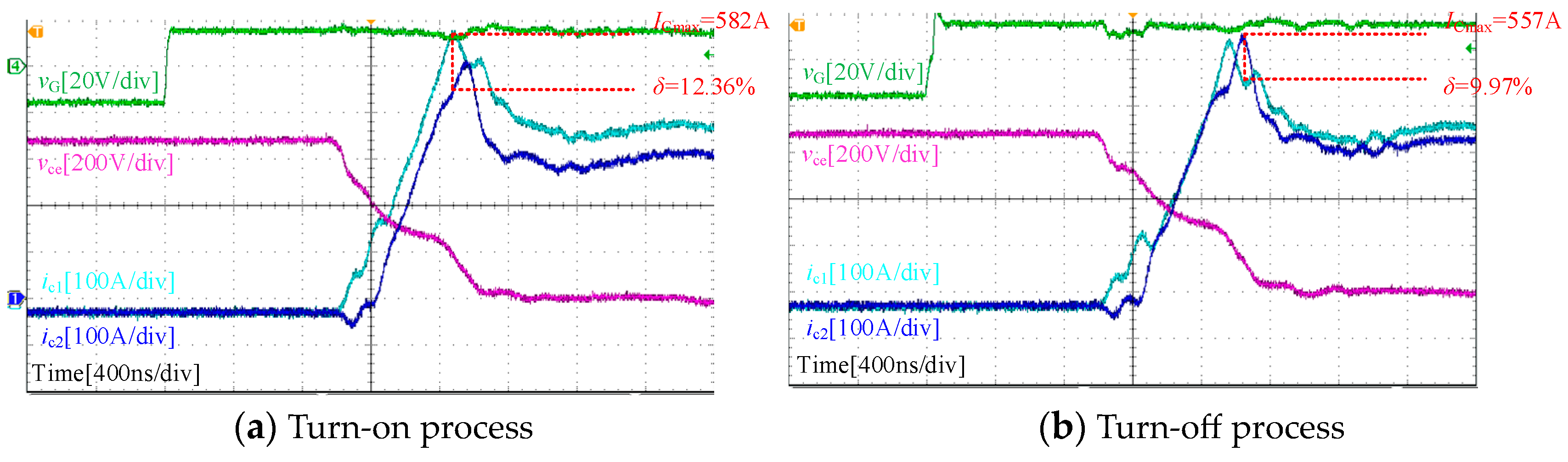
4. Characteristic Parameter Identification and Current Sharing Experiment

4.1. Characteristic Parameter Identification

In this paper, two FF300R17KE3 modules produced by Infineon are used as the tested objects. Through the parameter verification and identification method in this paper, the difference range of the characteristic parameters of the gate drive circuit of the two IGBTs is measured, which provides a data basis for subsequent parallel experiments. The test platform sets the bus voltage to 900 V, the load inductance to 100 μH, the gate output of the upper tube of the IGBT module is −15 V to keep it off reliably, and the gate driver of the lower tube outputs a double pulse of 15 V/−15 V. We observed the voltage VG1 between G1 and AE, the voltage VG2 between G2 and AE, the collector current IC and the collector voltage VCE.
For the external resistance RG,ext, a high-precision LCR bridge is used to measure the resistance to obtain the external turn-on gate resistance RGon,ext and the external turn-off gate resistance RGoff,ext. For the internal RG,int, the resistance is obtained by measuring the platform voltages VG2(pl)on and VG2(pl)off and the gate currents IG,on and IG,off of the voltages between G2 and AE during the turn-on and turn-off process.By substituting them into Formulas (23) and (24), the gate turn-on resistance RG,on and the gate turn-off resistance RG,off can be obtained by combining the measured external resistance.
For the equivalent gate capacitance CGE, the turn-on delay phase can be obtained by measuring the waveform during the turn-on process. The matching gate capacitance can be calculated using Formula (25). For the equivalent gate-collector capacitances CGC1 and CGC2, the turning voltage takes the maximum point of VCE rising slope curvature considering the VCE rising waveform during the turn-off process. When it is substituted into Formula (26), the equivalent capacitance of the Miller plateau can be calculated. Table 1 summarizes the extraction results of the four modules’ gate drive loop characteristic parameters.

4.2. Current-Sharing Experiment

In the experiment, the two tested FF300R17KE3 half-bridge IGBT modules T1 and T2 paralleled by parameter extraction were used for double-pulse experiments. The experimental hardware circuit is shown in Figure 13. We observed the current distribution of the two modules during the turn-on and turn-off process, as shown in Figure 14a, and calculated the compensation value of the turn-on process to be 27.6. It can be seen that the current rise rate of module 1 in the turn-on process before the synchronous variable-amplitude drive compensation is introduced is larger, consistent with the calculation results and theoretical analysis trends. Before the introduction of synchronous variable-amplitude drive control, the current unbalance degree in the opening process is 12.36%, and the current peak value is 582 A. At this time, the turn-off process is relatively current sharing, and the turn-on process needs to introduce synchronous variable-amplitude compensation.
Figure 14b is the experimental waveform result after adding synchronous variable-amplitude drive control, and the current unbalance degree at that point in time was 9.97%. It can be seen that the T1 tube is turned on first during the turn-on process, which leads to a greater current stress on the module when it is first turned on, a large rate of rise in the turn-on current, and an unbalanced current distribution in the dynamic process. When the collector current rises, the synchronous variable-amplitude drive control is added to adjust its current rising rate, so that its equivalent current rising rate is consistent with the No. 2 branch, and the current sharing effect of the synchronous variable-amplitude drive control is verified.
At the same time, the experimental verification is carried out through the current sharing effect of multiple groups of different gate drive voltages and action times, as shown in Figure 15. The dynamic characteristics of the turn-on process under the control of different gate control voltages and action times are the same as the analysis and simulation results.
As shown in Figure 16, the dynamic characteristics of the turn-off process under the control of different gate control voltages and action times are the same as the analysis and simulation results. It can be seen from the horizontal comparison that its control effect in the turn-off process is weaker than that in the turn-on process.
Similar to the simulation results, within a certain range of gate voltage amplitudes or action times, the current imbalance issue in parallel modules can be improved.

5. Conclusions

In this paper, the characteristic parameters of parallel dynamic current sharing are analyzed through simulation modeling and experiments, and the influence of characteristic parameters on parallel dynamic current sharing characteristics and the sensitivity under the same relative difference degree is obtained. A synchronous variable-amplitude driving method is proposed, which mainly includes the following:
  • Considering the relative difference of body parameters, the influence of each dynamic characteristic parameter on the parallel application of IGBT is analyzed, and the variation law is further analyzed through simulation. When selecting the parallel IGBT module, paying attention to the consistency of these characteristic parameters as much as possible can effectively improve the degree of parallel current sharing. The current difference and current integral value are proposed as the evaluation indexes of current sharing.
  • Through the verification and identification of the characteristic parameters, the characteristic parameters of the gate drive circuit that are not easy to obtain in the datasheet are modeled and analyzed, and the method of calculating the gate characteristic parameters through the experimental data of the turn-on and turn-off process is studied. This allows for the determination of the composite parameter differences between modules can be obtained so that IGBT modules with similar parameter characteristics are selected for parallel use and provide parameter basis for synchronous variable-amplitude drive compensation.
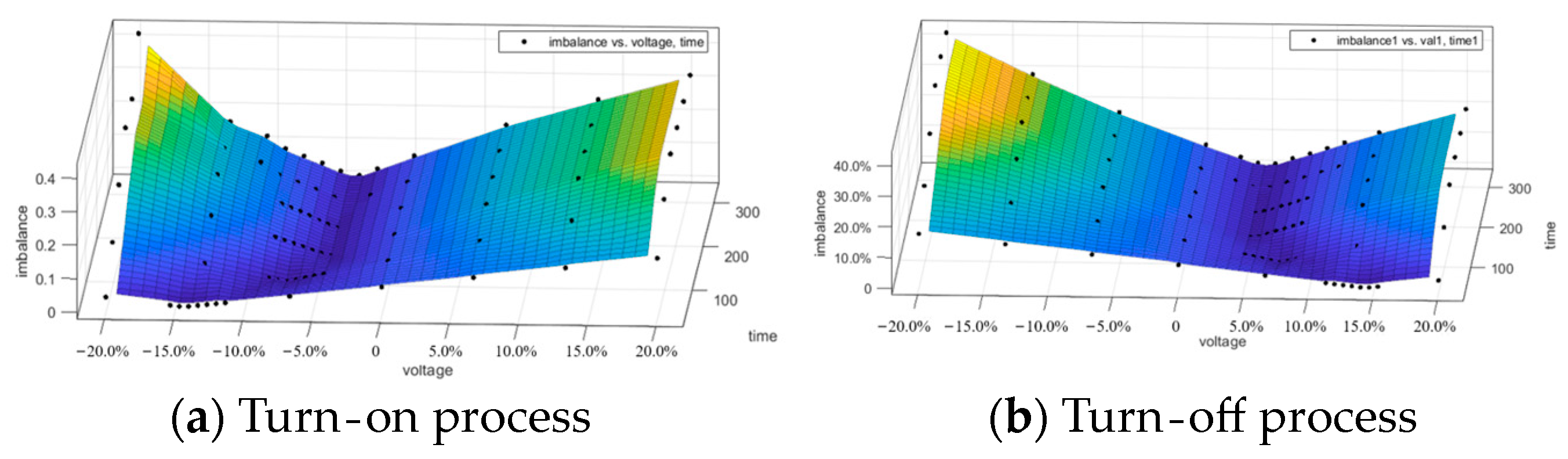
  • A synchronous variable-amplitude driving method is proposed, and the working principle of this method is clarified in conjunction with the dynamic process circuit model. The effectiveness of this method is verified by simulation. And through multiple sets of simulations, the three-dimensional relationship among gate control voltage, action time, and current unbalance degree is fitted.
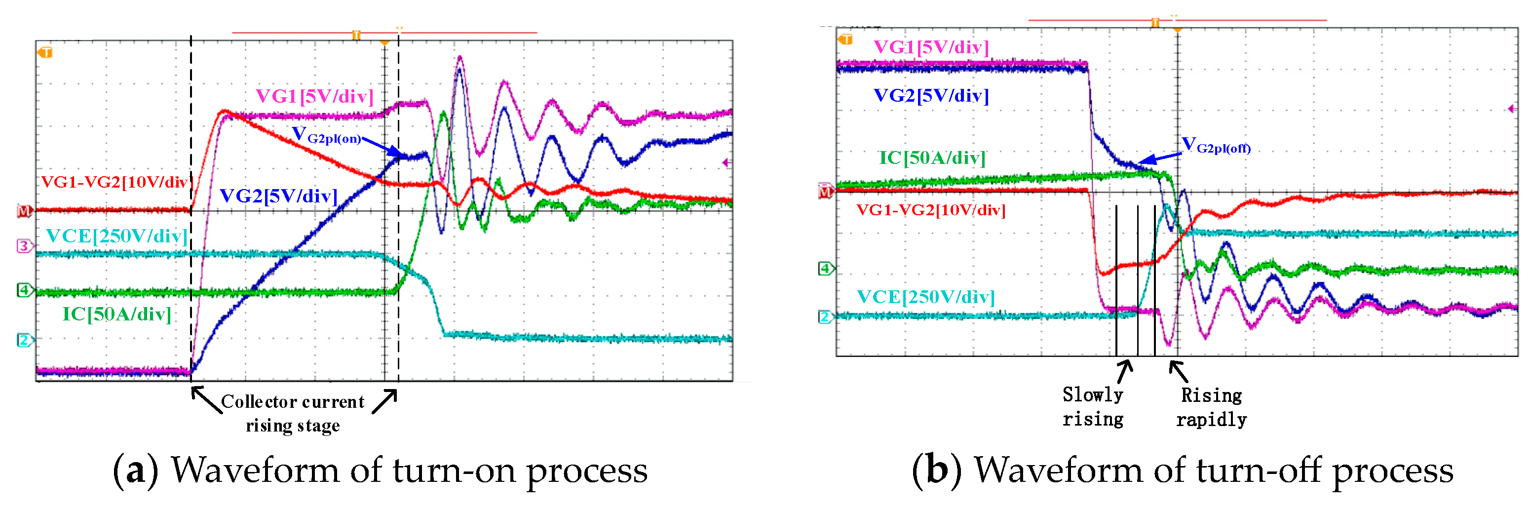
  • Based on the obtained characteristic parameters of two sets of IGBT modules, synchronous and asymmetric drive compensation was performed, leading to an improvement in current equalization characteristics. This validated the effectiveness of the method. Furthermore, the impact of different gate control voltages and action times on the dynamic current equalization characteristics of parallel operation was further verified. This provides a theoretical basis for subsequent parallel experiments.

Author Contributions

Conceptualization, J.Z. and C.X.; methodology, E.L. and C.X.; validation, J.Z. and L.J.; formal analysis, K.M. and Y.L.; data curation, X.L. and X.W.; writing—original draft preparation, E.L.; writing—review and editing, J.Z.; supervision, C.X.; project administration, E.L.; funding acquisition, J.Z. All authors have read and agreed to the published version of the manuscript.

Funding

This work was supported by the Scientific and Technological Projects of China Southern Power Grid Company, Ltd. under Grant GDKJX M20212014.

Data Availability Statement

No new data were created.

Conflicts of Interest

The authors declare no conflict of interest.

Notations

SymbolDescriptionUnit
VCE(sat)the collector voltageV
iCthe collector currentA
VGE(th)the gate voltageV
Tjthe junction temperature°C
tdelaythe signal transmission delay timems
VG,onthe gate turn-on voltageV
VG,offthe gate turn-off voltageV
RG,onthe gate turn-on resistanceΩ
RG,offthe gate turn-off resistanceΩ
RG,intthe gate module internal resistanceΩ
CGCthe gate collector capacitancenF
CGEthe gate emitter capacitancenF
LGthe gate inductancemH
LCthe collector inductancemH
LEthe emission pole inductancemH
RCthe collector resistanceΩ
REthe emitter resistanceΩ
Ciesxthe input capacitor of branch xnF
VGExthe gate voltage of branch xV
iCxthe collector current of branch xA
RGx,onthe gate resistor of branch xΩ
VCExthe collector voltage of branch xV
VGE(th)xthe turn-on threshold voltageV
CGExthe gate-emitter capacitor of branch xnF
tnthe time pointms
VGx,onthe turn-on drive voltage used by the drive control circuitV
VGx,offthe turn-off drive voltage used by the drive control circuitV
RGx,onthe sum of the external drive resistanceΩ
td(on)xthe turn-on delay timems
LExthe auxiliary emitter inductancemH
Kthe equivalent transconductance-
gfsxthe forward transfer rate-
VCCthe initial gate control voltageV
VG1the gate control voltageWb/m2
Irrthe equivalent current overshootA
VGE(pl)xthe Miller plateau voltageV
Vosthe voltage overshootV
ΔIcthe collector current differenceA
δthe degree of current imbalance-
RG,extthe external resistanceΩ
εthe curvature-

References

  1. Ma, L.; Zhang, D.; Yang, G.; Xie, S.; Ouyang, L.; Wei, H. Research on the IGBT Paralleling Application. High Power Convert. Technol. 2015, 2, 35–39. [Google Scholar] [CrossRef]
  2. Matallana, A.; Andreu, J.; Garate, J.I.; de Alegria, I.M.; Kortabarria, I. Analysis of impedance and current distributions in parallel IGBT design. In Proceedings of the 2017 IEEE 26th International Symposium on Industrial Electronics (ISIE), Edinburgh, UK, 19–21 June 2017; pp. 616–621. [Google Scholar] [CrossRef]
  3. Spang, M.; Katzenberger, G. Current sharing between parallel IGBTs in power modules during short circuit with unsymmetrically connected load. In Proceedings of the 2016 18th European Conference on Power Electronics and Applications (EPE’16 ECCE Europe), Karlsruhe, Germany, 5–9 September 2016; pp. 1–9. [Google Scholar] [CrossRef]
  4. Zhang, G.; Liu, Z.; Wang, L.; Quan, H. Parallel Technologies of Power module for Traction Power Supply with Energy Feedback. Trans. China Electrotech. Soc. 2010, 25, 78–82. [Google Scholar]
  5. Liu, J.; Hao, X.; Wang, X.; Chen, Y.; Fang, W.; Niu, S. Application of thyristor controlled phase shifting transformer excitation impedance switching control to suppress short-circuit fault current level. J. Mod. Power Syst. Clean Energy 2018, 6, 821–832. [Google Scholar] [CrossRef] [Green Version]
  6. Wissen, M.; Domes, D.; Brekel, W.; Yilmaz, K. How asymmetric busbar design causes symmetric switching behavior of paralleled IGBT modules. In Proceedings of the CIPS 2018; 10th International Conference on Integrated Power Electronics Systems, Stuttgart, Germany, 20–22 March 2018; pp. 1–3. [Google Scholar]
  7. Kong, L.; Zhang, D.; Puqi, N.; Zhang, J.; Qiu, Z. The IGBT module layout design considering the electrical and thermal performance. In Proceedings of the 2014 IEEE Conference and Expo Transportation Electrification Asia-Pacific (ITEC Asia-Pacific), Beijing, China, 31 August–3 September 2014; pp. 1–5. [Google Scholar] [CrossRef]
  8. Martin, C.; Schanen, J.; Guichon, J.; Pasterczyk, R. Analysis of Electromagnetic Coupling and Current Distribution Inside a Power Module. IEEE Trans. Ind. Appl. 2007, 43, 893–901. [Google Scholar] [CrossRef]
  9. Zhang, C.; Sun, C.; Ma, W.; Ai, S. Paralleling Current Sharing Method of Parallel IGBTs Based on Circuit Topology. High Volt. Eng. 2013, 39, 505–512. [Google Scholar]
  10. Wang, J.M.; Yan, Q.H.; Dong, L.; Xiao, G.D.; Yan, Z.M.; Hu, J.S.; Wang, Y. Research on dynamic current sharing of parallel high-power IGBTs. Electr. Autom. 2010, 32, 10–12. [Google Scholar]
  11. Weigel, J.; Boehmer, J.; Wahl, E.; Nagel, A.; Krafft, E.U. Paralleling of High Power Dual Modules: Standard Building Block Design for Evaluation of Module Related Current Mismatch. In Proceedings of the 2018 20th European Conference on Power Electronics and Applications (EPE’18 ECCE Europe), Riga, Latvia, 17–21 September 2018; pp. P.1–P.10. [Google Scholar]
  12. Wissen, M.; Domes, D.; Brekel, W.; Holtij, T.; Groove, A. Effects of Influencing the Individual Leg Inductance in Case of Paralleling Modules on Basis of XHP 3 and EconoDUAL. In Proceedings of the PCIM Europe 2017; International Exhibition and Conference for Power Electronics, Intelligent Motion, Renewable Energy and Energy Management, Nuremberg, Germany, 5–7 June 2017; pp. 1–6. [Google Scholar]
  13. Alvarez, R.; Bernet, S. A new delay time compensation principle for parallel connected IGBTs. In Proceedings of the 2011 IEEE Energy Conversion Congress and Exposition, Phoenix, AZ, USA, 17–22 September 2011; pp. 3000–3007. [Google Scholar] [CrossRef]
  14. Matallana, A.; Andreu, J.; Garate, J.I.; Aretxabaleta, I.; Planas, E. Analysis and modelling of IGBTs parallelization fundamentals. In Proceedings of the IECON 2016—42nd Annual Conference of the IEEE Industrial Electronics Society, Florence, Italy, 23–26 October 2016; pp. 3247–3252. [Google Scholar] [CrossRef]
  15. Tang, Y.; Ma, H. Dynamic Electrothermal Model of Paralleled IGBT Modules with Unbalanced Stray Parameters. IEEE Trans. Power Electron. 2017, 32, 1385–1399. [Google Scholar] [CrossRef]
  16. Huang, X.; Mu, F.; Liu, Y.; Wu, Y.; Sun, H. Asynchronous Gate Signal Driving Method for Reducing Current Imbalance of Paralleled IGBT Modules Caused by Driving Circuit Parameter Difference. IEEE Access 2021, 9, 86523–86534. [Google Scholar] [CrossRef]
  17. Schlapbach, U. Dynamic paralleling problems in IGBT module construction and application. In Proceedings of the 2010 6th International Conference on Integrated Power Electronics Systems, Nuremberg, Germany, 16–18 March 2010; pp. 1–7. [Google Scholar]
  18. Jadhav, V.; Zhou, Y.; Jansen, U. Analysis of Different IGBT Gate Driver Strategies Influencing Dynamic Paralleling Performance. In Proceedings of the PCIM Asia 2016; International Exhibition and Conference for Power Electronics, Intelligent Motion, Renewable Energy and Energy Management, Shanghai, China, 28–30 June 2016; pp. 1–9. [Google Scholar]
  19. Peng, C.; Li, X.; Fan, J.; Zhao, Z.; Tang, X.; Cui, X. Experimental investigations on current sharing characteristics of parallel chips inside press-pack IGBT devices. IEEE Trans. Power Electron. 2022, 37, 10672–10680. [Google Scholar] [CrossRef]
  20. Li, Z.F.; Nishida, N.; Aoki, H.; Shibata, H.; Liao, C.C.; Huang, M.S. Simulation-Assisted Design of a Power Stack for Improving Static Current Sharing Among Three IGBT Modules Connected in Parallel. IEEE Access 2022, 10, 10079–10093. [Google Scholar] [CrossRef]
  21. Wang, Y.; Wang, J.; Liu, F.; Liu, Q.; Zou, R. An RLL current sharing snubber for multiple parallel IGBTs in high power applications. IEEE Trans. Power Electron. 2022, 37, 7555–7560. [Google Scholar] [CrossRef]
  22. Zeng, X.; Li, Z.; Wan, J.; Zhang, J.; Ren, M.; Gao, W.; Li, Z.; Zhang, B. Embedded hardware artificial neural network control for global and real-time imbalance current suppression of parallel connected IGBTs. IEEE Trans. Ind. Electron. 2019, 67, 2186–2196. [Google Scholar] [CrossRef]
  23. Lu, J.; Shen, L.; Huang, Q.; Sun, D.; Li, B.; Tan, Y. Investigation of a rectangular heat pipe radiator with parallel heat flow structure for cooling high-power IGBT modules. Int. J. Therm. Sci. 2019, 135, 83–93. [Google Scholar] [CrossRef]
  24. Yuan, W.; He, Y.; Li, Z.; Ruan, Y.; Lu, L.; Li, B. A real-time aging monitoring method of parallel-connected IGBT modules. Mater. Sci. Semicond. Process. 2021, 124, 105555. [Google Scholar] [CrossRef]
Figure 1. Circuit diagram of the parallel IGBT application circuit diagram including characteristic parameters affecting current sharing.
Energies 16 05306 g001
Figure 2. The principle of synchronous variable-amplitude driving method.
Energies 16 05306 g002
Figure 3. Dual-module parallel equivalent circuit model and process waveform.
Energies 16 05306 g003
Figure 4. Equivalent schematic diagram of turn-on current rise rate.
Energies 16 05306 g004
Figure 5. Equivalent schematic diagram of turn-off current rise rate.
Energies 16 05306 g005
Figure 6. Simulation results of the influence of relative errors of different parameters on the switching process.
Energies 16 05306 g006
Figure 7. The influence of different parameters on the opening and closing process. (Each triangle represents a data point).
Energies 16 05306 g007
Figure 8. Comparison pre- and post-sync amplitude drive control in turn-on process.
Energies 16 05306 g008
Figure 9. Comparison pre- and post-sync amplitude drive control in turn-off process.
Energies 16 05306 g009
Figure 10. The three-dimensional relationship among drive control voltage, action time, and current unbalance degree in the turn-on and turn-off process. (The darker the color, the smaller the degree of current imbalance, while the lighter the color, the larger the degree of current imbalance.)
Energies 16 05306 g010
Figure 11. IGBT module parameter extraction circuit.
Energies 16 05306 g011
Figure 12. Experimental waveform of characteristic parameter extraction of IGBT module.
Energies 16 05306 g012
Figure 13. The experimental hardware circuit of the synchronous variable-amplitude drives method.
Energies 16 05306 g013
Figure 14. Waveform results of the parallel experiment of the two modules without compensation.
Energies 16 05306 g014
Figure 15. The control effect of VG1 and tC1 on the turn-on process.
Energies 16 05306 g015
Figure 16. The control effect of VG2 and tC2 on the turn-on process.
Energies 16 05306 g016
Table 1. Transmission extraction results of characteristic parameters of the gate drive circuit of each module.
Parameter NameParameter Values
Test ConditionsVDC = 900 V, IL = 250 A
IGBT Modules1700 V−11700 V−2
RG,int2.41 Ω2.33 Ω
RG,on4.41 Ω4.65 Ω
RG,off4.39 Ω4.35 Ω
CGE28.98 nF29.92 nF
CGC19.17 nF9.29 nF
CGC20.62 nF0.64 nF
Disclaimer/Publisher’s Note: The statements, opinions and data contained in all publications are solely those of the individual author(s) and contributor(s) and not of MDPI and/or the editor(s). MDPI and/or the editor(s) disclaim responsibility for any injury to people or property resulting from any ideas, methods, instructions or products referred to in the content.

