1. Introduction
Perovskite materials have great potential for high efficiency in photovoltaic devices. The best performances are today close to 26% in single junction and 33% in tandem with silicon [
1]. Organic–inorganic hybrid halide perovskites possess properties interesting for optoelectronic applications, such as tunable band gap, low exciton binding energy, high absorption coefficient, high electron and hole mobilities, and long carrier diffusion length [
2]. This generation of photovoltaic systems emerged as part of a third generation after noting the high cost of energy production needed for the first generation based on Si semiconductors and the high toxicity, low abundance or high cost of the elements for the most efficient systems of the second generation (CIS, CIGS, CdTe, and GaAs). This is why, over the last 20 years, semiconductors with photo-electrical properties compatible with high photovoltaic efficiencies and at affordable costs have been developed, including organic/polymer, dye-sensitized, quantum dot, and hybrid perovskite solar cells. The latter have been hugely successful and have seen some of the fastest growth in solar cell performance together with a great potential for industrialization due to the low cost of raw materials and to the ease of perovskite manufacturing methods [
3].
We now need to further develop device architectures that combine simple industrial development with effective durability. Traditionally used perovskite solar cell architectures can be either based on planar or mesoscopic architectures [
4] and are divided into two categories: standard (NIP) and inverted (PIN) [
5]. This depends on which transporting layer (electron or hole) is receiving firstly the incident light. Recently, a novel type of architecture emerged for which no hole transport layer is needed. Indeed, as carbon electrodes can extract photo-generated holes by themselves, this makes it possible to manufacture more stable perovskite solar cells without commonly used organic hole-transporting layers [
6,
7,
8]. In addition, traditional metal electrodes can also decrease the perovskite solar cell durability due to the potential formation of silver and gold halides when used with perovskite [
9,
10]. Consequently, the use of carbon-based perovskite solar cells (C-PSC) with inexpensive and stable carbon electrodes not only enhances the durability of the devices but also reduces fabrication costs [
5].
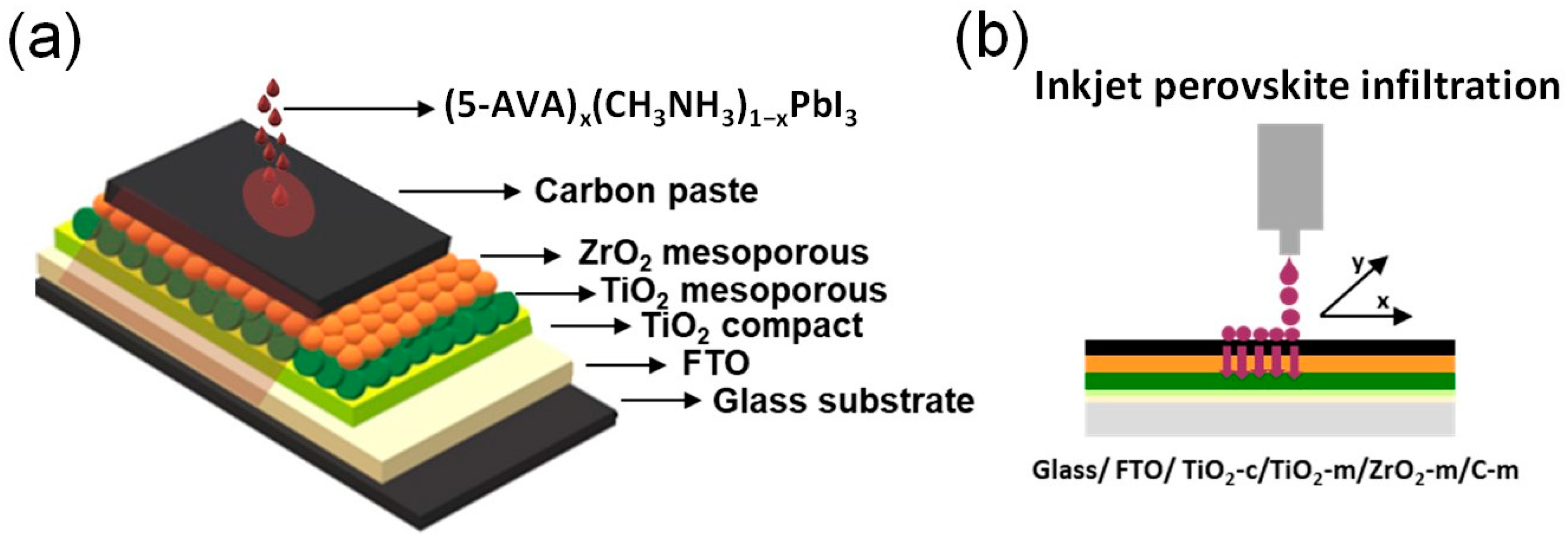
Figure 1a presents the architecture of here studied C-PSC devices. A typical carbon-based perovskite solar cell consists of a front FTO/glass substrate, a mesoporous electron transporting layer, an insulating intermediate layer and then the mesoporous carbon electrode [
11]. In this architecture, the intermediate insulating layer is crucial to prevent contact between the front and back electrodes, thus avoiding ohmic shunts and photocurrent leakage [
10]. The most common insulating mesoporous materials used are ZrO
2 [
12] and Al
2O
3 [
13]. ZrO
2 generally possesses larger pores than Al
2O
3 which facilitate the infiltration of the perovskite and, thus, makes it a more efficient spacer material for C-PSC. Such perovskite solar cells also offer great potential for easy recycling. Bogachuk et al. [
14] and Ku et al. [
15] demonstrated that the triple mesoporous scaffold (TiO
2/ZrO
2/Carbon) can be reused after perovskite removal by washing.
Another main advantage of this C-PSC architecture is that the perovskite precursors can be incorporated by simple injection within the mesoporous stack (m-TiO
2/m-ZrO
2/m-Carbon) after the fabrication of the entire stack. This clean method of perovskite deposition allows us to eliminate the need for a glove box during device manufacturing, which greatly facilitates their industrial development, unlike other predominantly developed perovskite device architectures. The more commonly referenced method for perovskite insertion involves a single large central drop deposition [
7,
16]. In this paper, this step will be upgraded using inkjet printing as illustrated in
Figure 1b to enable a fully industrial process [
17].
Perovskite solar cells do not always achieve their maximum efficiency after perovskite deposition and annealing, but sometimes require an additional procedure. Maturation is a process that improves the solar cell’s photovoltaic parameters and therefore its performance. This step can occur in the solar cell during manufacturing or can be imposed by external factors [
16]. The devices we obtained presented the specificity to undergo a large maturation after being exposed to a post-treatment at 40 °C with 75% RH for 150 h. This increases the power conversion efficiency (PCE) from 10% to 14%, leading to a close to 40% relative increase in PCE. This PCE enhancement could not be obtained by varying the traditional annealing step duration or temperature. In addition, other tentative post-treatment conditions did not work as well as the 40 °C/75%RH condition. Increasing either the temperature, humidity or time conduct to either similar or lower results. According to the literature, similar or higher improvement rates could be obtained with dark storage at 40 °C under vacuum (relative increase in PCE = 35% for CH
3NH
3PbI
3 and 60% for chlorinated CH
3NH
3PbI
3) [
18]. However, the reported devices and perovskite architectures were different from the present work and the observed enhancement was not transferable to our systems. Regarding other remarkable positive but lower maturation conditions reported on devices with close architecture, we can list: a 13% PCE enhancement after 500 h of storage in dark and vacuum conditions [
17]; a 9% PCE enhancement after 150 h of UV light soaking (eq. 1.5 sun UV illumination; 40 °C, open-circuit condition) [
19]; and a 16% PCE enhancement after 10 min at 1 sun illumination (25 °C, load-circuit condition) [
20].
A full study of the underlying mechanisms was thus conducted for the selected maturation conditions using a complete set of characterization techniques: J-V measurements, UV–visible and PL spectroscopies, LBIC and PL imaging, XRD, and surface roughness measurements. In addition, it seems interesting to us to investigate the impact of this maturation step on the performance’s durability. Such valuable information is typically lacking in the existing literature for other types of maturation phenomena.
2. Materials and Methods
2.1. Studied Materials: Perovskite Solar Devices Fabrication
The architecture of the typical monolithic carbon-based, hole transport layer-free, perovskite solar cells, produced by Solaronix S.A. (Aubonne, Switzerland), and studied in this manuscript consists of a front FTO/glass substrate (TCO22-7/LI, Solaronix low-iron soda-lime glass coated with a 7 Ohm/sq. fluorine-doped tin oxide layer of about 500 nm, electrode size: 25 × 20 mm), electron-selective layers to avoid the non-radiative recombination at the front electrode (TiO2 compact and mesoporous layers), a mesoporous ZrO2 insulating layer to avoid ohmic shunts and a mesoporous carbon back electrode.
An 18 ± 3 nm compact layer of TiO2 was deposited by spray pyrolysis over the FTO glass substrates of titanium diisopropoxide bis(acetylacetonate) diluted in ethanol at 450 °C. A 550 ± 75 nm thick mesoporous TiO2 layer was then obtained by screen-printing a nanoparticle paste (Ti-Nanoxide T165/SP, Solaronix), followed by a 45 min firing at 500 °C. Similarly, a 1 ± 0.1 μm thick mesoporous ZrO2 layer was obtained by screen-printing a nanoparticle paste (Zr-Nanoxide ZT/SP, Solaronix) followed by firing at 500 °C. Finally, a 17 ± 1.5 μm conductive porous carbon electrode was obtained by screen-printing a high-temperature graphite/carbon paste (Elcocarb B/SP, sheet resistivity: ≤25 ohm/sq, Solaronix) followed by 30 min firing at 400 °C, affording a 12.5 × 12.0 mm active area. Thicknesses were measured by mechanical profilometry after each deposition step. The perovskite precursor solution is added at the end using the inkjet deposition method.
The perovskite precursor solution (5-AVA)xMA1−xPbI3 (reference 76802, Solaronix) in gamma-butyrolactone (GBL) solvent containing lead iodide (PbI2) and methylammonium iodide (MAI) in equimolar concentration (1.2 mol/mL) with 5 mol% of 5-ammoniumvaleric acid iodide (5-AVAI) was transferred to an inkjet printer cartridge. Then, a total quantity of 3.85 µL was infiltrated all over the TiO2/ZrO2/Carbon filled area with a drop-on-demand inkjet printer (PixDro LP50, 512 nozzle printhead) at a resolution of 1200 × 1200 dpi. The samples were annealed for 10 min on a hot plate set to 50°C to form the desired perovskite crystal structure.
The fresh solar cells were eventually exposed to a post-treatment in order to achieve maximal performance. This maturation step was performed at 40 °C with a 75% RH atmosphere for 100–150 h. For these purposes, full photovoltaic devices were deposited in a closed box containing a round dish filled with a saturated NaCl solution [
21], and the box was deposited in an oven settled at 40 °C in a dark environment.
A 1.8 mm thick soda-lime glass lid was used as the back glass. It was sealed to the front glass with a Surlyn gasket (SG) using a vacuum membrane laminator with an integrated pump, programmable heat and duration (1 atmosphere pressure).
Table 1 presents the reference and characteristics of the used SG sealant.
2.2. Aging Campaigns Conditions
To compete with other PV technologies and to investigate the solar cells’ long-term stability for commercial desires, the aging behavior of the devices has been evaluated. According to International Electrotechnical Commission test standards (IEC 61215), the only test accepted by both module manufacturers and buyers (for silicon devices) is an exposition of solar devices to air atmosphere at 85 °C with 85% of relative humidity. In this paper, the so-called damp heat test has been used: encapsulated solar cells have been aged in a humidity chamber (HCP150, Memmert, set at 85 °C and 85% R.H.). Cells were aged in the same orientation as for end-use operating conditions, i.e., transparent FTO electrode side up. Regular sampling of cells was realized to monitor certain functional and/or structural properties. The aim was to track relevant aging markers in order to determine the degradation mechanisms involved.
2.3. Characterizations
J-V measurements were recorded under illumination with a solar light simulator Newport Oriel LCS-100 providing an AM 1.5 G spectrum of 1000 W·m−2 light intensity and using an SP-50 potentiostat/galvanostat from Biologic (France). The J-V measurements were performed in reverse mode from Voc to −0.2 V at a 4 mV/s scan rate.
To measure the layer thicknesses, each layer was measured (Stack 1: FTO+TiO2-c; Stack 2: FTO+TiO2-c+TiO2-m; Stack 3: FTO+TiO2-c+TiO2-m+ZrO2; and Stack 4: FTO+TiO2-c+TiO2-m+ZrO2+Carbon) with a KLA Tencor model D500 profilometer after scratching a line with a scalpel in the samples’ center. The roughness of Stack 4 without or with perovskite filling and before or after maturation was also measured using the profilometer. For each given value, a total of nine profiles on three different samples were made. The measurement range used with this equipment was: 2.5 μm for the three first stacks, 10 μm for the fourth one and for complete cells with the infiltrated perovskite layer. A scan speed of 0.05 mm·s−1 and a force equivalent to 0.2 mg were applied, together with 10,000 data points in each profile with a filter-level average equal to 4 points.
UV–visible diffuse absorbance spectra were measured with a UV-2600 spectrophotometer (Shimadzu, France) equipped with an integrating sphere accessory. Absorbance measurements require a previous step of carbon paste (CP) removal. Indeed, the opacity of the thick CP layer avoids any possible transmission of light within the entire device. This was performed using the adhesive scotch peeling method and could present the disadvantage to remove also a small quantity of the perovskite layer.
The photoluminescence (PL) spectra of studied solar cells were obtained using a RF-6000 spectrofluorometer (Shimadzu, France) with a 520 nm excitation wavelength using a scan rate of 6000 nm/min, an excitation slit of 5 nm, an emission slit of 5 nm and a measurement range of 600–900 nm. Two filters were used: a 575 nm low-pass in front of the excitation source and a 600 nm high-pass in front of the source of emission in order to suppress any artifact coming from the spectrophotometer.
XRD analyses of perovskite layers were performed on opened cells (after peeling of CP) using a X’Pert PRO MPD X-ray diffractometer (PANalytical, France) from the Consortium of Common Technological Means (CMTC in Grenoble, France) between 2-theta of 8° and 50° with Cu-Ka source. After extraction of the background and integration of all contributions, the relative crystallinity of the studied perovskite and the PbI2 amount present in the perovskite were evaluated.
For light beam-induced current (LBIC) mapping, a homemade apparatus was developed. It involves a 532 nm (5 mW) laser diode with a 0.7 mm width beam, set on a computer-controlled X-Y moving stage. As the surface of the cell is scanned, the output current is metered using a source measure unit (2602 Keithley, Cleveland, OH, USA). Scanning the entire active area of the cell lasts more or less 20 min.
Luminescence imaging was also carried out using a homemade device consisting of a camera equipped with a 650 nm high-pass filter and a 525 nm green diode, inside a dark box. Complete devices were characterized in open circuit condition. As the signal obtained varied according to acquisition conditions (time, aperture, etc.), which did not allow a quantitative comparison of the noted changes, a calibration reported in previous papers was used [
22]. Image processing (cropping, coloring or thresholding) was carried out using the free ImageJ software (version 1.8.0).
3. Results and Discussion
The perovskite ink used is a solution of methylammonium lead iodide (MAPbI
3) perovskite precursors with 5 mol% of 5-ammonium valeric acid iodide (5-AVAI). MAPbI
3 is the most commonly used perovskite with a direct-like bandgap between 1.5 and 1.6 eV [
23,
24]. The latter additive is known to improve the formation of the MAPbI
3 perovskite crystals into the mesoporous layers, generating a preferential growth in the normal direction, which is important for thick perovskite layers as in our C-PSC architecture (>1 μm). According to the literature, the obtained mixed 2D/3D obtained perovskite is also reported to present better stability than pure 3D MAPbI
3 [
7,
8]. In addition, all other constituting layers of the device are inorganic and therefore very stable.
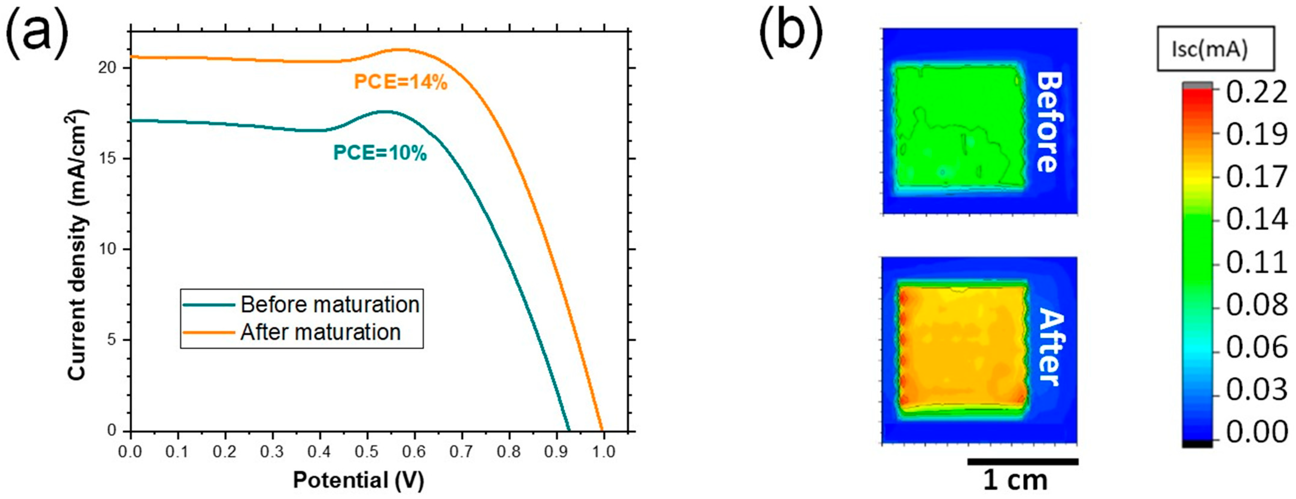
The different photovoltaic parameters (average value and standard deviation) here obtained for nine cells batches for both matured and non-matured devices are presented in
Table 2, and
Figure 2a presents the typical J-V curves obtained for both freshly processed solar cells (green) and the same devices exposed to the additional post-treatment (orange). It illustrates the maturation phenomenon observed through an improvement of the J-V curve affording higher PCE, which is related to both higher Jsc and Voc. It could be noticed that both J-V curves present an unusual “hump” pattern. As previously reported in the literature [
25], this pattern could be attributed to charge and discharge effects near TiO
2. To minimize this phenomenon, a particular slow scan rate was used here (4 mV/s).
Figure S1 in Supplementary Materials presents the comparison between both reverse and forward curves. It can be seen that the hysteresis and also the “hump” phenomena are less pronounced after maturation.
Figure 2b presents light beam-induced current (LBIC) images and certifies that the enhancement after maturation is quite homogeneous all over the active surface.
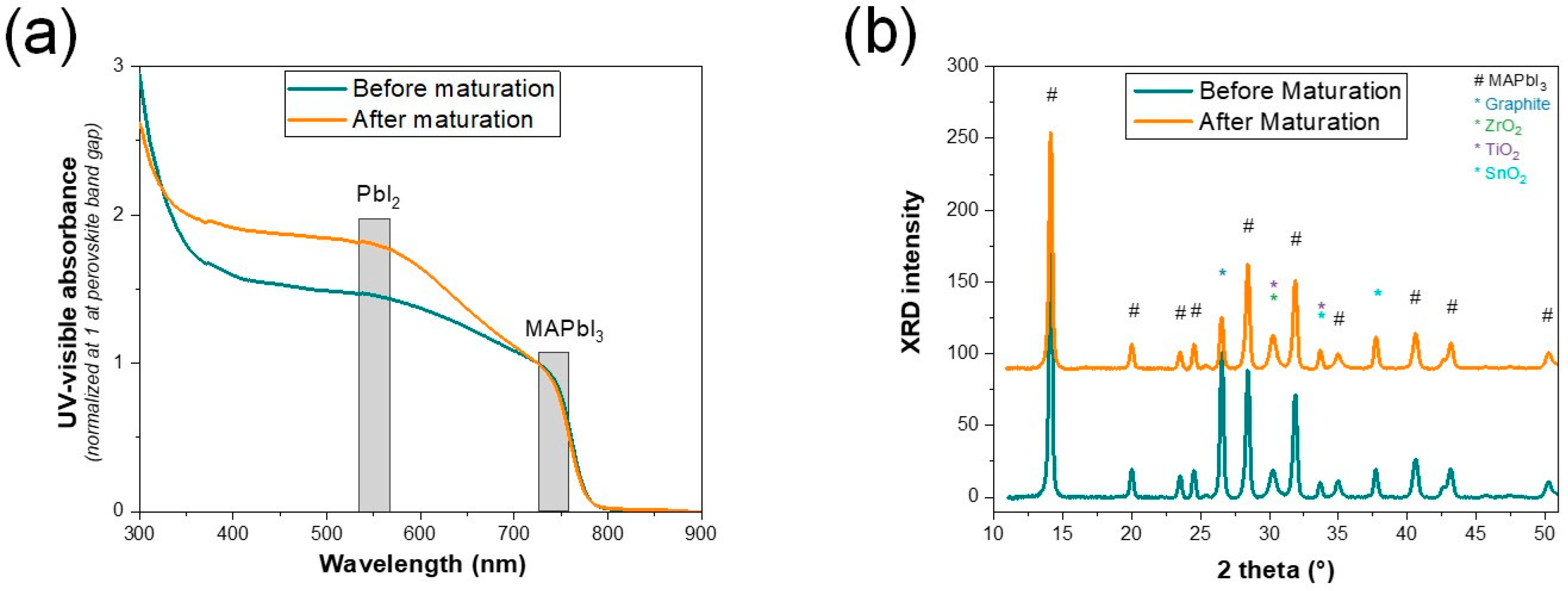
As a first step, the possible changes within the perovskite layer were scouted using UV–visible absorption and X-ray diffraction (XRD) presented in
Figure 3a,b, respectively. For these two analyses, the carbon paste layer was peeled off just before the analyses in order to better reveal the sole perovskite. If the perovskite band gap (1.59 eV) and the crystalline phases were strictly equal, some changes occurred within the perovskite material. After maturation, an increase in the PbI
2 peak was observable on absorption spectra. This was not correlated to the appearance of a PbI
2 peak in XRD diffractograms, indicating the presence of an amorphous PbI
2 phase. In addition, the perovskite relative crystallinity was found to decrease from 18 to 15%. At first sight, this is a degradation of perovskite compatible with exposure to humidity. It is however known that a small amount of PbI
2 can play the role of passivating agent and be beneficial for PV performances [
26]. This will be scouted using the following photoluminescence and roughness measurements.
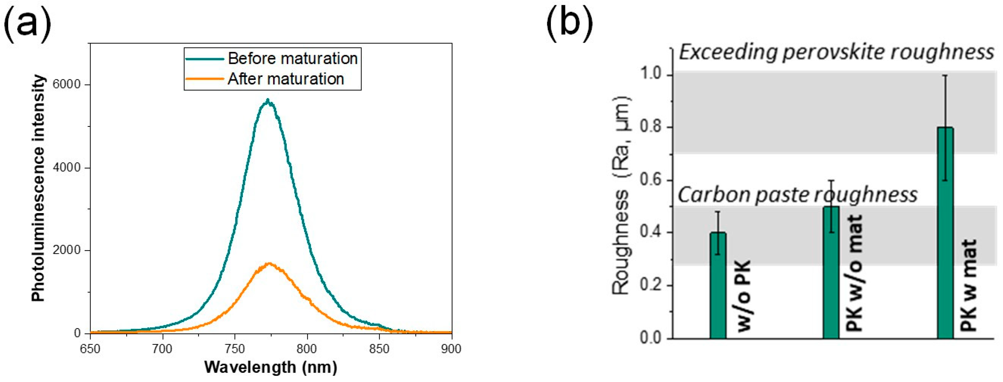
The positive impact of the maturation step is, however, confirmed by a significant decrease in photoluminescence emission highlighted in
Figure 4a. This PL reduction probably results from an improvement of the interfaces, with a recombination rate of the charge carriers decreasing due to better activation of the quenching effects at the interfaces [
27]. According to the literature [
28], both PL quenching and perovskite degradation can lead to a decrease in PL intensity that cannot be distinguished by PL characterization alone. This is because the PL signal only provides information about the radiative recombination of charge carriers, which is not sufficient to understand the full picture of photophysics. In addition, perovskite degradation is often responsible for an increase in PL [
27], proposed to be due to the passivation of charge traps responsible for PL quenching in perovskite crystals [
28]. PL data must therefore always be related to other observations such as PCE modifications.
In order to support previous conclusions,
Figure 4b presents roughness measurements realized on the top carbon electrode before and after maturation. It can be observed that before maturation the roughness is close to virgin carbon paste (i.e., 0.5 ± 0.1 μm vs. 0.4 ± 0.08 μm, which is quite equivalent), and then the value increases after maturation (0.8 ± 0.2 μm). As the perovskite precursor solution is infiltrated through the mesoporous layer, some perovskite could remain within carbon and the increase in roughness can be considered as evidence of either a small perovskite reorganization or a small perovskite passivation in PbI
2 compatible with an enhancement of the perovskite/carbon interface. The series resistance was also observed to be reduced by the maturation step (14.95 ± 1.36 Ω·cm
2 before and 9.45 ± 0.07 Ω·cm
2 after; see
Table 2 and
Figure S3), which is in accordance with an improvement of the perovskite materials and/or its interfaces.
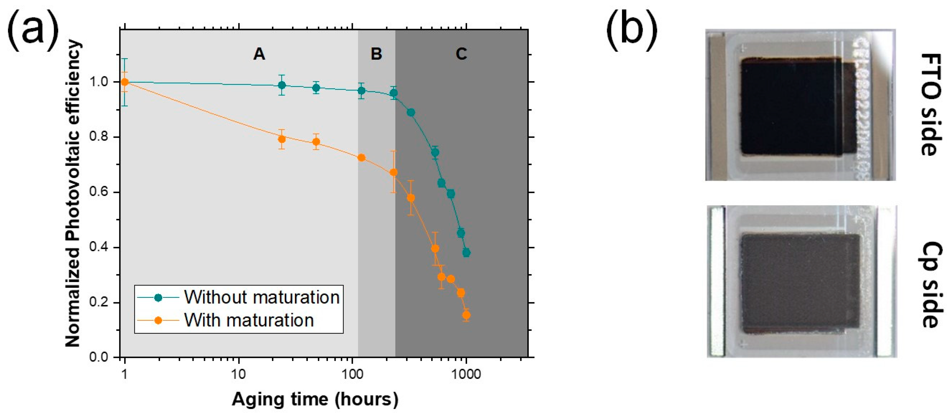
The second objective of the present study is to evaluate the impact of the maturation step on the long-term stability of these solar cells. For this purpose, glass–glass encapsulated cells (laminated using a Surlyn
® gasket) were subjected to an accelerated aging test during 1000 h using damp heat 85 °C/85%RH conditions. The evolution of the normalized PCE according to aging time for both matured and non-matured devices is presented in
Figure 5a, together with photographs of the devices encapsulated right before the aging campaign in
Figure 5b. For matured devices (orange), a significant decrease in performances was observed during the first days of aging, while the performances of non-matured devices (green) were relatively stable (defined as Phase “A”). This decrease appears to be mainly due to a decrease in J
sc (see
Figure S3 in Supplementary Materials). For all tested solar cells, the R
s value was relatively weak during this stage. Between 100 and 200 h of aging (zone named “B”), both type of devices processes equivalent performances, as highlighted in the non-normalized PCE evolution represented in
Figure S2 in Supplementary Materials. After this, a continuous decrease in performance can be observed whatever the initial treatment. It is the Phase named “C”. After 1000 h of aging, all cells show performances too low to be qualified as functional. However, we can note a more important degradation of the performances for the matured cells than the non-matured ones (for both normalized or non-normalized representations of PCE evolution). This decrease in performance is partly explained by the decrease in J
sc, which is also more important for the matured cells, correlated at the end of aging by a drastic increase in the R
s. The FF and V
oc parameters were globally quite stable during the 1000 h of aging (see
Figure S3 in Supplementary Materials). In conclusion, it could be hypothesized that the initial presence of passivating PbI
2 in matured cells acts as an accelerator of device aging.
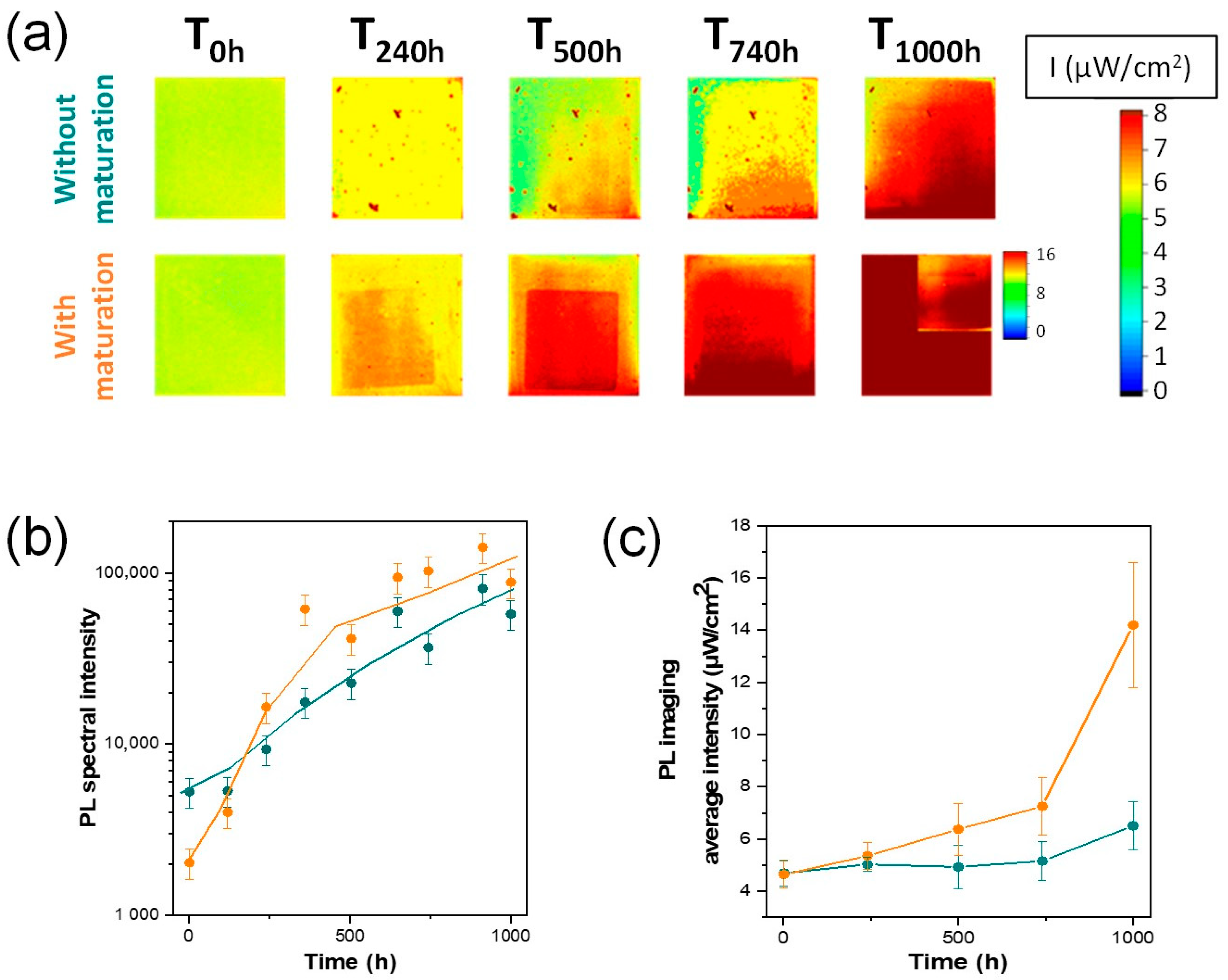
The photovoltaic results were combined with photoluminescence imaging monitoring, presented in
Figure 6a. PL imaging photos were taken from the FTO side, and the color scale represents the photoluminescence intensity variation. Homogeneous photoluminescence irradiance levels were found at T0 all over the surface whatever the system studied. During aging, some defaults and heterogeneities were revealed. In addition, a specific phenomenon was detected for matured devices. Indeed, the PL images reveal the J-V solicited area as a square shape caused by the mask used during J-V measurements. This more solicited area undergoes faster aging affording in this square the color corresponding to the following sampling point. This “special block” clearly appears for matured devices after 240 h of aging when the PCE begins its sharp decline. It is present for non-matured devices only slightly at 1000 h. We can assume that the fact to perform J-V characterizations is able to accelerate the degradation of an already largely degraded device. This could be due to either the solicitation by the 1 sun illumination and/or additional heating due to charge transfer within a defective perovskite layer.
In addition, according to
Figure 6b,c, we can observe that PL imaging data are in line with PL spectral data. Both follow an inverse trend than the PCE variation, i.e., the more the PL increase, the more the PCE decrease.
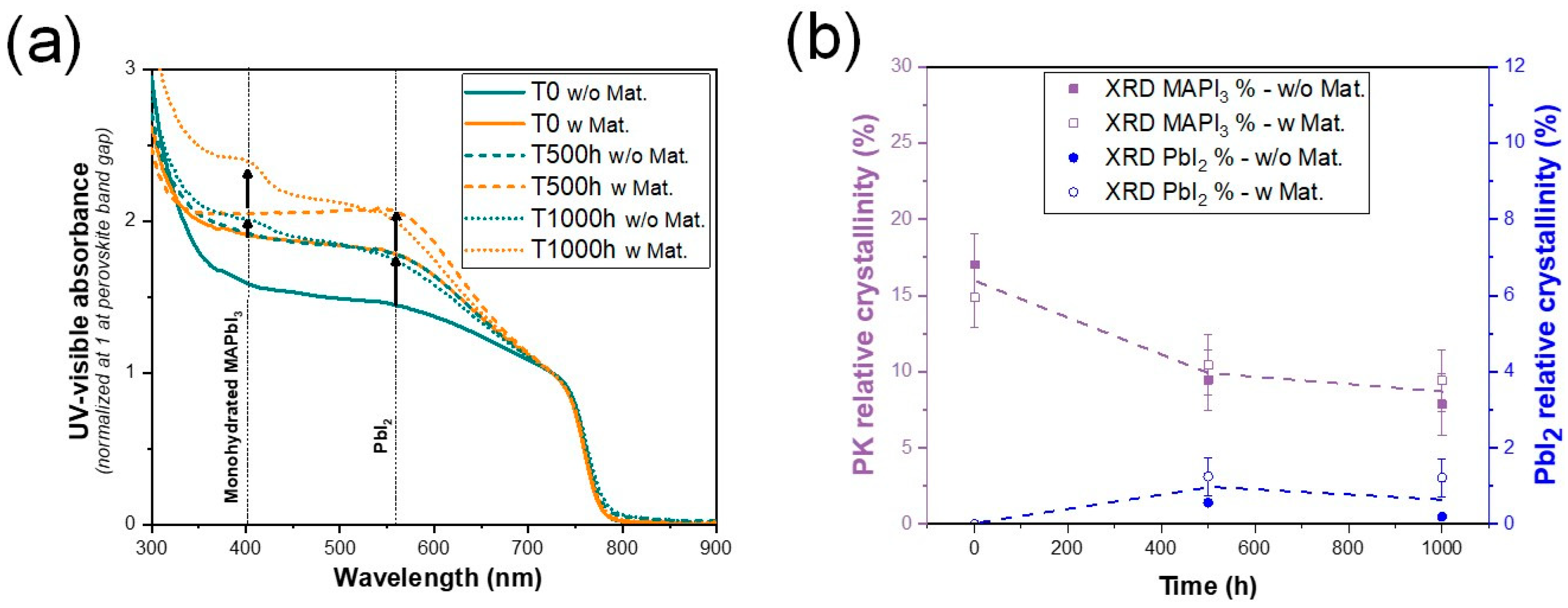
To better understand the performance variations observed, additional analyses were performed on both matured and non-matured opened solar cells after peeling the carbon layer; see absorption spectra in
Figure 7a and data extracted from XRD diffractograms in
Figure 7b (examples of full XRD diffractograms are presented in
Figure S4 in Supplementary Materials). No changes were identified in the perovskite band gap during aging and the perovskite phases are still present at the end of aging. Indeed, due to cell architecture configuration, the insulating ZrO
2 layer can lead to an insulating device even if partially filled with perovskite. During the first stages of aging, an intensification of the PbI
2 peak around 550 nm was observed for both solar cells (leading to a perfect superposition of the non-matured absorption spectra at 500 h with the matured spectra at 0 h). In another hand, at 500 h a peak of crystalline PbI
2 is evidenced in XRD, lightly more important for matured devices, in agreement with absorbance data. Both UV–visible absorption and XRD data confirm the previous hypothesis, i.e., the initial presence of passivating PbI
2 in matured cells accelerates the devices aging by a more rapid increase in the PbI
2 amount during the aging. Then, between 500 and 1000 h, XRD diffractograms do not vary considerably, but a second transition emerges on UV–visible spectra at 400 nm for both types of cells. The latter is attributed to the formation of monohydrated perovskite [
29,
30], and should most likely result from the permeation of water through the encapsulation sealing gasket. The hydrated perovskite visible in UV–visible absorption spectra could be in an amorphous or crystalline state; however, its crystalline presence was slightly detectable by XRD around 2θ = 10° [
29]; see
Figure S4 in Supplementary Materials.


 ,
, 


