Article

Application of TiO2/Ag/TiO2 as an Ohmic Contact to an AlGaAs Layer in a GaAs Solar Cell

1
Central Laboratory of Solar Energy and New Energy Sources, Bulgarian Academy of Sciences, 72 Tzarigradsko Chaussee Blvd, 1784 Sofia, Bulgaria
2
Central Laboratory of Applied Physics, Bulgarian Academy of Sciences, 61 Sanct Petersburg Blvd, 4000 Plovdiv, Bulgaria
3
Physical Sciences, Munster Technological University, Rosa Avenue, Bishopstown, Cork, Ireland and Tyndall National Institute, Lee Maltings, T12 R5CP Cork, Ireland
*
Author to whom correspondence should be addressed.
Energies 2023, 16(10), 4050; https://doi.org/10.3390/en16104050
Submission received: 9 March 2023 / Revised: 22 April 2023 / Accepted: 10 May 2023 / Published: 12 May 2023
(This article belongs to the Special Issue Advanced Materials and Structures for Photovoltaic Applications)

Abstract

:
This paper investigates the possibility of using a nanolaminate TiO2/Ag/TiO2 structure as a transparent conductive coating on GaAs solar cells. A novel result is that this structure forms an Ohmic contact to Al-rich AlGaAs, which is used as a “window” layer in GaAs-based solar cells. The TiO2/Ag/TiO2 structure is deposited by RF magnetron sputtering at room temperature. This nanolaminate coating has good optical and electrical properties: a high transmittance of 94% at 550 nm, a sheet resistance of 7 Ω/sq, and a figure of merit (FOM) of 105 × 10−3 Ω−1. These properties are the result of the presence of a discontinuous layer of Ag between two thin layers of TiO2. The morphology of a discontinuous layer of Ag nanogranules is confirmed by the observation of a cross-section of a sample with high-resolution transmission electron microscopy (HRTEM) and EDX analyses. Current–voltage diode characteristics of GaAs solar cells measured under standard test illumination at 1000 W/m2 are analyzed. The formation of an Ohmic contact is explained by the Fermi-level pinning effect caused by nanosized Ag particles in the nanolaminate TiO2/Ag/TiO2 structure. The obtained results demonstrate a new application of oxide−metal−oxide (OMO) coatings as Ohmic contacts to III-V compound semiconductors.

1. Introduction

In all semiconductor devices, metal–semiconductor contact plays a critical role in their performance and reliability. The contact systems can be divided into two subcategories: Schottky and Ohmic. The main difference is that the current–voltage characteristic of the Schottky contact is asymmetric, whereas that of the Ohmic contact is linear with respect to the different polarities of the applied voltage. There are several ways to form Ohmic contacts. One possible approach is to use a metal with a lower work function than that of the respective semiconductor. Another possibility is to form a thin, highly doped layer that is the same material as that of the substrate. The third possible solution is to use the effect known as Fermi-level pinning. This effect can be observed when high-density surface states are formed at the metal–semiconductor interface. Their occupation by electrons tends to pin the center of the band gap to the Fermi level. The fourth possible solution is to apply an alloyed interfacial layer between the metal and the semiconductor after high-temperature treatment. This approach is used when it is necessary to form an Ohmic contact with multi-component semiconductors of the AlGaAs [1] or AlGaN [2] type.
The contacts are essential parts of GaAs-based solar cells. The quality of the metal–semiconductor system plays a key role in the efficiency of the solar cells. However, it is difficult to obtain sufficiently low-resistivity Ohmic contacts to n-AlGaAs layers unless a highly doped n-type GaAs cap layer is used. This is especially true when the Al content in the AlGaAs cap layer is increased, as it becomes more difficult to obtain good Ohmic contacts with low resistivity.
The first study of WSix/p+-(Al)GaAs contacts was reported in [3]. Later, a PtTiGePd multilayer system on AlGaAs as a function of temperature treatment was studied in [1]. The obtained results showed that the low contact resistance achieved at 600 °C was due to As out-diffusion and the new compositional and structural uniformity of the interfacial layer between the metal structure and AlGaAs. The formation of Pd/Ge/Ti/Au and Au/Ge/Ni/Au Ohmic contacts to undoped AlGaAs, which was obtained by annealing at 450 °C, was reported as well [4]. It is assumed that this is due to the deep penetration of Au atoms. These atoms react with the substrate and form Au-Al and Au-Ga bonds that act as donors. A similar problem exists with Ohmic contacts to Al-rich AlGaN. The Ohmic contacts are a result of the intermetallic phase formation between the V/Al/Ni/Au metal stacks on AlGaN after high-temperature annealing [5].
In our previous study, we demonstrated an application of a TiO2/Ag/TiO2 nanolaminate structure, which has the properties of a transparent conductive coating [6]. The optoelectrical properties of the OMO nanolaminate structure are explained by the presence of metal nanoparticles that are spatially located between the two thin oxide layers [7]. A possible application of this structure as a transparent electrode was reported in [8,9,10]. Several transparent conductive coatings have been proposed: metal nanowires [11], carbon nanotubes [12], metal meshes [13], and conductive polymers. However, OMO multilayer electrodes are considered to be the state of the art [14,15].
This study investigates the application of a TiO2/Ag/TiO2 nanolaminate structure as an electrode that creates an Ohmic contact with an alloy semiconductor, such as AlGaAs, without using high-temperature annealing. The idea is to prove the effectiveness of metal nanoparticles, which create conditions for Fermi-level pinning. For this purpose, a GaAs-based solar cell with a wide-bandgap AlGaAs layer on the front side is used. The formation of a transparent Ohmic contact directly on the AlGaAs “window” greatly simplifies the manufacturing technology needed for GaAs solar cells by avoiding complicated and expensive photolithography processes.

2. Materials and Methods

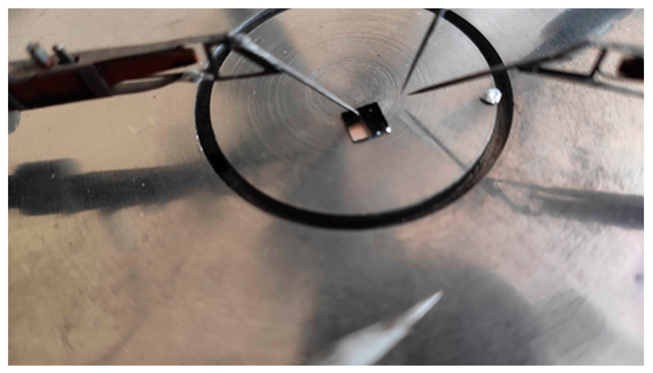
2.1. Solar Cell Structure

The schematic epitaxial structure of the single-junction GaAs solar cell with a nanolaminate TiO2/Ag/TiO2 transparent electrode on the surface is shown in Figure 1a. It is a commonly used double-heterostructure (DH) solar cell in which a p-n homojunction in GaAs is embedded between two wide-bandgap AlGaAs layers. The photo-recycling process in a DH allows increasing the effective minority-carrier lifetimes in GaAs and enhancing the internal quantum efficiency of the cell [16,17,18]. A thick AlGaAs layer is used as a back surface field (BSF) under the n-GaAs base region. To increase the light absorption in the GaAs photoactive region, a thin (30–40 nm) wide-bandgap “window” AlGaAs layer with at least 80% of Al content is grown on the top surface of the cell. In addition, the minority-carrier recombination rate at the AlGaAs/GaAs interface is significantly lower than that on the GaAs surface.
Since it is technologically difficult to obtain an Ohmic contact to the wide-bandgap AlGaAs layer, usually a thin, highly doped p++ GaAs layer is additionally grown on top of the AlGaAs window layer. The front grid metallization pattern is formed via the photolithography process, which is followed by annealing. To reveal the wide-bandgap window layer, the heavily-doped GaAs cap layer is selectively etched (Figure 1b).
The formation of a top Ohmic contact by deposition of a nanolaminate TiO2/Ag/TiO2 structure directly on the AlGaAs “window” layer reduces the technological steps and tools required, including the complicated and expensive photolithography process.
The AlGaAs/GaAs heterostructures were grown via low-temperature liquid-phase epitaxy (LPE) in a horizontal quartz tube using the multiple bin “piston” boat technique. In order to obtain a planar uniform structure, the crystallization was performed with a Ga-melt only 0.5 μm thick on an n-GaAs:Si substrate with dimensions of 15 mm × 30 mm. The 6N, Ga, and Al metals with a high purity and pieces of monocrystalline undoped GaAs wafers were used as sources for epitaxial growth. Sn was used as the n-type dopant for the BSF AlGaAs and n-GaAs base layers, while Mg was used as a dopant for the p-GaAs emitter and the p-AlGaAs “window”. After loading, the graphite boat was annealed for 1 h at a temperature that was about 100 °C above the epitaxy temperature in a stream of high-purity hydrogen to homogenize the melt and reduce background impurities and contamination. The crystallization was carried out from an initial temperature of 680 °C at a cooling rate of 1 °C/min. The p-n junction was formed at 560 °C and the wide-bandgap “window” layer on the surface was grown at 510 °C.
The back contact of the structure was formed by Ag magnetron sputtering and annealed at 500 °C for 20 min. An optically transparent and conductive nanolaminate TiO2/Ag/TiO2 structure was deposited directly on the wide-bandgap “window” AlGaAs layer of GaAs solar cells as a front contact. Solar cell samples with an area of 3 × 3 mm2 were cut from the structure.

2.2. Deposition of Nanolaminate OMO Structure

The technological procedure for obtaining the OMO nanolaminate structure was identical to that used in [6,7,19]. The deposition process consisted of high-frequency magnetron sputtering. A high-frequency (13.6 MHz) magnetron sputtering system model, the CFS-4ES Tokuda system (Tokuda, Seisakusho Co., Ltd., Ginan-cho, Japan), was used. The vacuum chamber was equipped with 3 positions of the 3-inch target. A water-cooled disk with a diameter of 200 mm was the substrate holder. The substrate holder and targets were positioned vertically. The distance between them was 8 cm. It is technically possible to mount three targets at eccentric positions in front of the substrate holder. In front of each target, there is a shutter that can be opened and closed without opening the vacuum chamber. In our magnetron sputtering process, two targets were used successively: Ag and TiO2, both with a purity of 99.9%. Argon was used as a sputtering gas. The chamber pressure before the deposition was approximately 1 × 10⁻⁶ mbar and the sputtering process was performed at a chamber pressure of approximately 6 × 10⁻³ mbar for TiO2 and 1 × 10⁻³ mbar for Ag.
The technological sequence was as follows: (i) the shutter in front of the TiO2 target was opened and a layer of titanium dioxide was deposited; (ii) the shutter in front of the Ag target was opened and a layer of silver was deposited; (iii) the shutter of the Ag target was closed and the shutter in front of the TiO2 target was opened to sputter a second layer of titanium dioxide. The RF power for the deposition of TiO2 was 200 W. During the sputtering process, the substrate holder was rotated at speeds of 20 rpm for TiO2 and 60 rpm for Ag. The deposition time and thickness of the layers of the nanolaminate TiO2/Ag/TiO2 structure are given in Table 1.

2.3. Characterization Methods

Optical transmittance and reflectance spectra were extracted with a UV–VIS–NIR Shimadzu 3600 double-beam spectrophotometer (Shimadzu, Japan) in the spectral region of 240–1200 nm with a resolution of 0.1 nm. The transmittance was measured against air and the reflectance was measured by using the specular reflectance attachment (5° incidence angle) and an Al-coated mirror as reference. The transmittance and reflectance spectra of a bare glass substrate are given as reference.
A Woollam M-2000 spectroscopic ellipsometer (J.A. Woollam Co. Instruments, Lincoln, NE, USA) was used to measure the TiO2 layers’ thickness on the Si substrate. The determination of the thickness of the ultrathin Ag layer was more complicated due to the inhomogeneous nature of the island structure. Therefore, some researchers use the duration of the sputtering process [20].
The properties of the TiO2/Ag/TiO2 structure as a transparent conductive coating were evaluated using the Haacke method [21]. The figure of merit was determined by using the transmittance T at 500 nm and the sheet resistance Rsh. Table 2 presents the obtained results for the figure of merit.
TEM analysis was performed with the JEOL 2100, 200 kV (JEOL Ltd., Tokyo, Japan), which has a double-tilt holder, and the beam was aligned at the {110} zone axis of the carrier wafer. The cross-section was made with the Helios Nanolab Dual-Beam FIB (CIC nanoGUNE, San Sebastian, Spain): final thinning at 93 pA and 30 kV, final polish at 5 kV and 56 pA, and in situ lift out. The high-angle annular dark-field (Z-contrast) imaging was conducted using the scanning transmission electron microscopy mode of the JEOL 2100F (200kV field-effect source microscope), which was equipped with EDAX energy-dispersive X-ray spectroscopy system for elemental mapping.
AFM measurements were made with an MFP-3D Origin instrument. The images were taken in tapping mode. In the presented measurements, an area of 2 µm × 2 µm was scanned, with a scan rate of 1.0 Hz and an image resolution of 256 × 256 dots. In the experiment, silicon probes with a cantilever length of 240 um and a Ti/Ir coating on both the back side and the tip (ASYELEC.01-R2) were used. These probes have a nominal cantilever resonant frequency of 75 kHz and a typical spring constant of 2.8 N/m. Image processing was carried out using Gwyddion 2.62.
An automatic measuring system under a standard test illumination at 1000 W/m2 was used to measure the I-V curve of the solar cell samples. The measuring probe was a micromanipulator that makes contact with the TiO2/Ag/TiO2 layer directly, as shown in Figure 2.

3. Results and Discussion

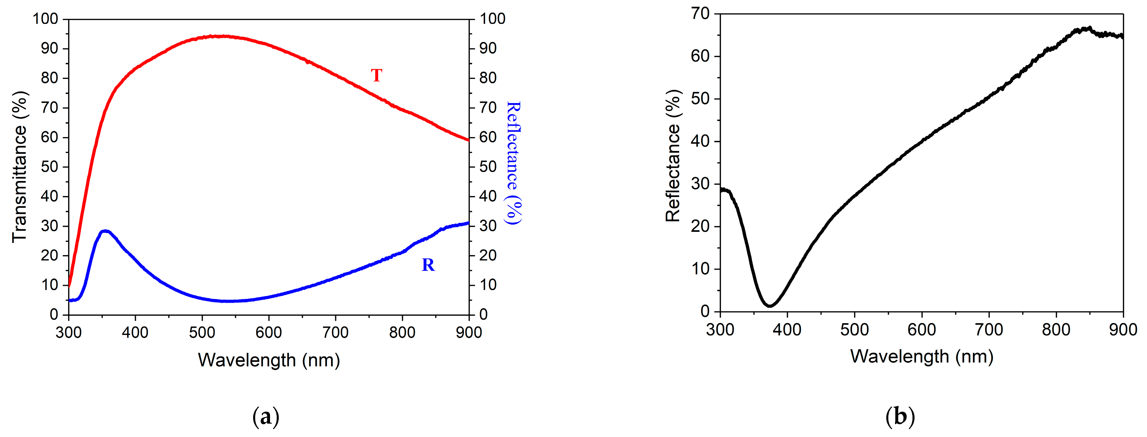
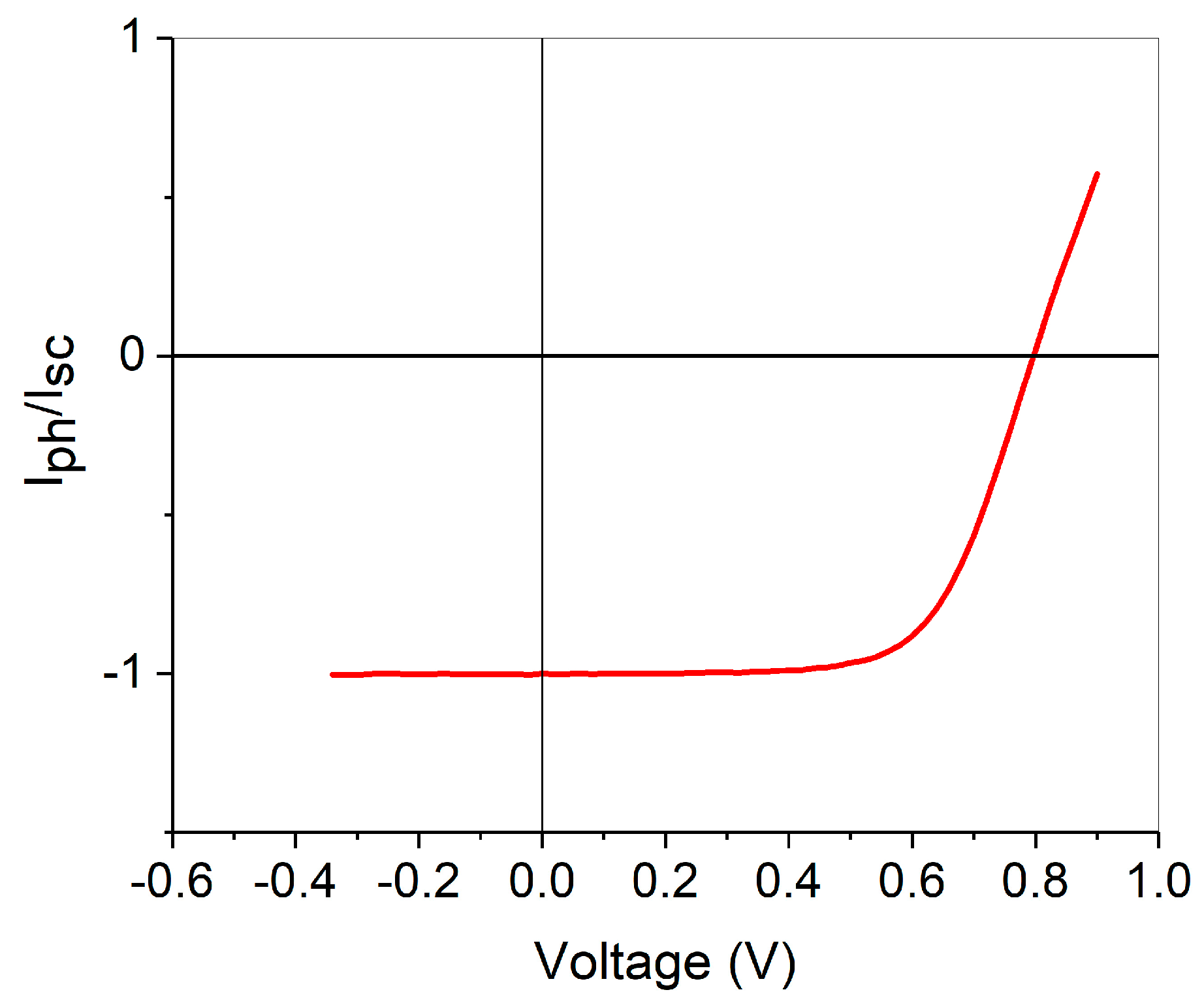
3.1. Optical and Electrical Properties of the Solar Cell Sample with TiO2/Ag/TiO2 Electrode

In Figure 3a, the transmittance and reflectance spectra of TiO2/Ag/TiO2 deposited on the glass substrate are presented. A high transmittance and low reflectance are revealed at the wide part of the wavelength range, around 400–800nm. However, when the TiO2/Ag/TiO2 is deposited on the top of the GaAs solar cells, the reflectance spectrum is determined by the reflectance of the AlGaAs surface, as shown in Figure 3b. Therefore, this laminate structure cannot be used as an antireflection coating.
Figure 4 shows a typical current–voltage characteristic of a sample under illumination. The measured values for the light-generated current are normalized to the maximum short-circuit current I/Isc. The use of the ratio I/Isc is intended to estimate the effect of the contact resistance of the sample, regardless of the absence of a grid electrode or the absence of an antireflection coating. The fill factor is known to be very sensitive to the contact resistance. The open-circuit voltage Voc is 0.8 V and the fill factor FF is determined to be 0.67. We obtained nearly the same fill factor value (F = 0.68) in our previous work [22] for a similar LPE grown structure with metal grid on the front surface. In the previous experiment [22], the device was bonded with a circuit board for a more accurate measurement. In its technological implementation, additional technological processes were used. Since it is difficult to make Ohmic contact with a wide-bandgap AlGaAs compound with high Al content, additional heavily doped p++ GaAs was grown on the “window” layer. The front grid metallization pattern was formed by the photolithography process. To reveal the wide-bandgap window layer, the heavily-doped GaAs cap layer was selectively etched.
The formation of an Ohmic contact by the direct deposition of a nanolaminate TiO2/Ag/TiO2 structure on the AlGaAs window layer greatly simplifies the technology required for realizing solar cells and gives additional advantages.
The application of a TiO2/Ag/TiO2 coating as a transparent electrode was reported in [23]. A bulk heterojunction organic solar cell fabricated with an optimized TiO2/Ag/TiO2 electrode showed higher power conversion efficiency than the same cell with an ITO electrode. The optimized electrode TiO2/Ag/TiO2 structure showed the greatest value for figure of merit. OMO structures that were used as transparent electrodes in optoelectronic devices were also reported [24,25,26,27,28].

3.2. TEM and AFM Characterization of Nanolaminate TiO2/Ag/TiO2 Structure

Our previous studies [7] have shown that the discontinuous morphology of the Ag layer is essential for developing the properties of our oxide–metal–oxide (OMO) nanolaminate structure.
The morphology of a nanogranular structure of Ag was confirmed via cross-section high-resolution transmission electron microscopy (HRTEM) observations. Figure 5 shows the TEM image of a larger area of the nanolaminate structure and depicts the layers formed, e.g., two layers of amorphous TiO2 and an inhomogeneous layer with Ag nanoparticles (NPs). The thickness, the aggregation density of Ag NPs, and their orientation in the plane of the substrate vary, as evidenced by the varying TEM contrast in the Ag layer.
This finding is also supported by EDX analysis, where the localization of the TiO2 layers is determined by the TiO2-spectral imaging map, whereas the Ag layer is identified in the Ag map (Figure 6). The Ag signal varies within the layer, suggesting varying aggregation densities of the Ag NPs within the layer.
A higher magnification lattice contrast image of Ag nanoparticles is presented in Figure 7. Besides confirming once more the presence of Ag NPs, their grain size in the layer, and their varying orientations, some twinning and other planar defects can be identified in the Ag layer. This is typical for Ag NPs when they are formed at a low temperature.
Figure 8a,b shows a top-view AFM image and 3D image of a silver layer deposited on a silicon surface with the same process used for the structure in Figure 5. The Ag island clusters with sizes of 50−100 nm are clearly distinguished. This corresponds to the results in [7,29] for thin layers obtained by magnetron sputtering of Ag in Ar. According to other studies, continuous Ag films with a thickness below 10 nm are typically not achievable.
The embedded metal granulates with dimensions around 100 nm are intended to improve the electrical conductivity of the OMO structure. In this range, quantum size effects begin to dominate, affecting the electronic and optical properties [30,31]. The nanolaminated TiO2/Ag/TiO2 structure with metal granulates demonstrates metallic conductivity because it has a positive temperature coefficient of resistance (TCR) [19]. Therefore, the carriers are delocalized due to thermal activation and conductivity is dominated by phonon scattering. The key parameter that determines most of the physical properties of the granular array is the average tunneling conductance between neighboring regions [32].
The new information about the electrical behavior of the TiO2/Ag/TiO2 coating is the formation of an Ohmic contact with the AlGaAs substrate. This can be explained by the presence of nanosized metal particles in the interface, which cause Fermi-level pinning. This assumption is supported by the results of the investigations of Fermi-level equilibration of nanoparticles with a polarized electrode, which were reported in [33]. We assume that the Fermi level of the nanoparticles may be raised or lowered via electron transfer with a polarized substrate. As the Fermi level of the substrate is controlled by the voltage source, the Fermi level of the nanoparticle is shifted to reach the Fermi level of the substrate.
Similar results for the electrical behavior of metallic nanoparticles were reported in [34]. The electrical contact of the Au nano-island structure in niobium-doped SrTiO3 was investigated. At Au nanoparticle sizes smaller than 45 nm, the transition from Schottky to Ohmic contact occurs [34].
In the context presented above, our results can be explained by the formation of an Ohmic contact through the Fermi-level pinning effect between the OMO coating and the AlGaAs layer of the solar cell structure.

4. Conclusions

This paper shows a new application of an oxide−metal−oxide (OMO) structure. The TiO2/Ag/TiO2 structure was studied as a transparent contact, which formed an Ohmic contact with AlGaAs. The research was performed on a GaAs-based solar cell. The front contact is realized with the TiO2/Ag/TiO2 nanolaminated structure. The solar cell is very sensitive to the contact resistance through the fill factor. The obtained results show that a good Ohmic contact with the AlGaAs layer was achieved. The advantage of the TiO2/Ag/TiO2 structure is that it can be used as a transparent conductive coating that forms an Ohmic contact with AlGaAs and has a high Al content. It is assumed that the presence of metal nanoparticles creates a condition for Fermi-level pinning. This concept can also be experimentally applied to other wide-bandgap semiconductors, such as GaN, AlGaN, etc. The properties of OMO multilayered electrodes can be modified by using other metals, such as Pt, Ni, or different metal oxides. The obtained results confirm that oxide–metal–oxide (OMO) transparent electrodes can be potential alternative contacts to III-V compound semiconductors.

Author Contributions

Conceptualization, P.V. and M.M.; methodology, P.V., M.M., and H.D.; investigation, H.D. and M.M.; formal analysis, N.P.; writing—original draft preparation, P.V and M.M.; writing—review and editing, N.P.; visualization, M.M.; supervision, P.V. All authors have read and agreed to the published version of the manuscript.

Funding

The authors acknowledge the financial support of project No. BG05M2OP001-1.002-0014, “Center of competence HITMOBIL—Technologies and systems for generation, storage and consumption of clean energy”, funded by the Operational Programme “Science and Education For Smart Growth”, 2014–2020, and co-funded by the EU via the European Regional Development Fund.

Acknowledgments

This work was supported by the European Regional Development Fund within the Operational Program “Science and Education for Smart Growth 2014–2020” under project № BG05M2OP001-1.002-0014, “Center of competence HITMOBIL—Technologies and systems for generation, storage and consumption of clean energy”, and Project CoE, “National centre of mechatronics and clean technologies”, BG05M2OP001-1.001-0008. The authors are grateful to K. Kirilov for help with the AFM measurements and T. Ivanova for help with the UV–VIS measurements.

Conflicts of Interest

The authors declare no conflict of interest.

References

  1. Cole, M.W.; Han, W.Y.; Casas, L.M.; Eckart, D.W.; Monahan, T.; Jones, K.A. The Mechanisms of Formation of Ohmic Contacts toAlGaAs: A Microstructural, Elemental Diffusion and Electrical Investigation. Scanning 1996, 18, 379–384. [Google Scholar] [CrossRef]
  2. Douglas, E.A.; Reza, S.; Sanchez, C.D.; Koleske, D.; Allerman, A.; Klein, B.; Armstrong, A.M.; Kaplar, R.J.; Baca, A.G. Ohmic contacts to Al-rich AlGaN heterostructures. Phys. Status Solidi (A) 2017, 214, 1600842. [Google Scholar] [CrossRef]
  3. Rabinzohn, P.; Usagawa, T.; Kobayashi, M.; Mishima, T.; Yaman, A. Low Resistance Refractory ohmic Contact to p+GaAs and p+AlGaAs. In Proceedings of the Conference on Solid State Devices and Materials, Tokyo, Japan, 24–26 August 1988; pp. 287–290. [Google Scholar]
  4. Choi, K.J.; Han, S.Y.; Lee, J.-L.; Moon, J.K.; Park, M.; Kim, H. Au/Ge/Ni/Au and Pd/Ge/Ti/Au Ohmic Contacts to AlxGa1-xAs/InGaAs Pseudomorphic High Electron Mobility Transistor. J. Korean Phys. Soc. 2003, 43, 253–258. [Google Scholar]
  5. Cho, H.K.; Mogilatenko, A.; Susilo, N.; Osterma, I.; Seifert, S.; Wernicke, T.; Kneissl, M.; Einfeldt, S. Electrical properties and microstructure of V/Al/Ni/Au contacts on n-Al0.65Ga0.35N:Si with different Au thicknesses and annealing temperatures. Semicond. Sci. Technol. 2022, 37, 105016. [Google Scholar] [CrossRef]
  6. Dikov, H.; Ivanova, T.; Vitanov, P. Oxide/metal/oxide nanolaminate structures for application of transparent electrodes. J. Phys. Conf. Ser. 2016, 764, 012021. [Google Scholar] [CrossRef]
  7. Vitanov, P.; Ivanova, T.; Dikov, H.; Terziyska, P.; Ganchev, M.; Petkov, N.; Georgiev, Y.; Asenov, A. Effect of a Discontinuous Ag Layer on Optical and Electrical Properties of ZnO/Ag/ZnO Structures. Coatings 2022, 12, 1324. [Google Scholar] [CrossRef]
  8. Su, Y.C.; Chiou, C.C.; Marinova, V.; Lin, S.H.; Dikov, H.; Vitanov, P.; Hsu, K.Y. Liquid crystal electro-optic modulator based on transparent conductive TiO2/Ag/TiO2 multilayers. Opt. Quantum Electron. 2018, 50, 242. [Google Scholar] [CrossRef]
  9. Chiou, C.C.; Hsu, F.H.; Petrov, S.; Marinova, V.; Dikov, H.; Vitanov, P.; Lin, S.H. Flexible light valves using polymer-dispersed liquid crystals and TiO2/Ag/TiO2 multilayers. Opt. Express 2019, 21, 1691. [Google Scholar] [CrossRef]
  10. Chengang, J.; Liu, D.; Zhang, C.; Guo, L.J. Ultrathin-metal-film-based transparent electrodes with relative transmittance surpassing 100%. Nat. Commun. 2020, 11, 3367. [Google Scholar]
  11. Deng, B.; Hsu, P.C.; Chen, G.; Chandrashekar, B.N.; Liao, L.; Ayitimuda, Z.; Wu, J.; Guo, Y.; Lin, L.; Zhou, Y.; et al. Roll-to-Roll Encapsulation of Metal Nanowires between Graphene and Plastic Substrate for High-Performance Flexible Transparent Electrodes. Nano Lett. 2015, 15, 4206–4213. [Google Scholar] [CrossRef]
  12. Hecht, D.S.; Hu, L.; Irvin, G. Emerging Transparent Electrodes Based on Thin Films of Carbon Nanotubes, Graphene, and Metallic Nanostructures. Adv. Mater. 2011, 23, 1482–1513. [Google Scholar] [CrossRef] [PubMed]
  13. Lee, J.Y.; Connor, S.T.; Cui, Y.; Peumans, P. Semitransparent Organic Photovoltaic Cells with Laminated Top Electrode. Nano Lett. 2010, 10, 1276–1279. [Google Scholar] [CrossRef] [PubMed]
  14. Kim, S.; Montero, J.; Yoon, J.; Choi, Y.; Park, S.; Song, P.; Osterlund, L. Embedded Oxidized Ag−Pd−Cu Ultrathin Metal Alloy Film Prepared at Low Temperature with Excellent Electronic, Optical, and Mechanical Properties. ACS Appl. Mater. Interfaces 2022, 14, 15756–15764. [Google Scholar] [CrossRef] [PubMed]
  15. Ferhati, H.; Djeffal, F. Performance Assessment of TCO/Metal/TCO Multilayer Transparent Electrodes: From Design Concept to Optimization. J. Comput. Electron. 2020, 19, 815–824. [Google Scholar] [CrossRef]
  16. Letay, G.; Hermle, M.; Bett, A.W. Simulating Single-junction GaAs Solar Cells Including Photon Recycling. Prog. Photovolt Res. Appl. 2006, 14, 683–696. [Google Scholar] [CrossRef]
  17. Wang, X.; Khan, M.R.; Gray, J.L.; Alam, M.A.; Lundstrom, M.S. Design of GaAs Solar Cells Operating Close to the Shockley—Queisser Limit. IEEE J. Photovolt. 2015, 3, 737–744. [Google Scholar] [CrossRef]
  18. Walker, A.W.; Hohn, O.; Micha, D.N.; Blasi, B.; Bett, A.W.; Dimroth, F. Impact of Photon Recycling on GaAs Solar Cell Designs. IEEE J. Photovolt. 2015, 5, 1636–1645. [Google Scholar] [CrossRef]
  19. Dikov, H.; Vitanov, P.; Ivanova, T.; Stavrov, V. Optical and electrical properties of nanolaminate dielectric structures. J. Phys. Conf. Ser. 2016, 700, 01205420. [Google Scholar] [CrossRef]
  20. Yu, X.; Zhang, D.; Wang, P.; Murakami, R.; Ding, B.; Song, X. The optical and electrical properties of ZnO/Ag/ZnO films on flexible substrate. Int. J. Mod. Phys.Conf. Ser. 2012, 6, 55–56. [Google Scholar] [CrossRef]
  21. Haacke, G. New Figure of Merit for Transparent Conductors. J. Appl. Phys. 1976, 47, 4086–4089. [Google Scholar] [CrossRef]
  22. Vitanov, P.; Milanova, M.; Goranova, E.; Dikov, C.; Ivanov, P.; Bakardjieva, V. Solar Cell Technology on the Base of III-V Heterostructures. J. Phys. Conf. Ser. 2010, 253, 012044. [Google Scholar] [CrossRef]
  23. Zhao, Z.; Alford, T.L. The optimal TiO2/Ag/TiO2 electrode for organic solar cell application with high device-specific Haacke figure of merit. Sol. Energy Mater. Sol. Cells 2016, 157, 599–603. [Google Scholar] [CrossRef]
  24. Kim, J.H.; Kim, D.H.; Seong, T.Y. Realization of highly transparent and low resistance TiO2/Ag/TiO2 conducting electrode for optoelectronic devices. Ceram. Int. 2015, 41, 3064–3068. [Google Scholar] [CrossRef]
  25. Kim, J.H.; Lee, J.H.; Kim, S.W.; Yoo, Y.Z.; Seong, T.Y. Highly flexible ZnO/Ag/ZnO conducting electrode for organic photonic devices. Ceram. Int. 2015, 41, 7146–7150. [Google Scholar] [CrossRef]
  26. Zhang, Y.; Liu, Z.; Ji, C.; Chen, X.; Hou, G.; Li, Y.; Zhang, X. Low-Temperature Oxide/Metal/Oxide Multilayer Films as Highly Transparent Conductive Electrodes for Optoelectronic Devices. ACS Appl. Energy Mater. 2021, 4, 6553–6561. [Google Scholar] [CrossRef]
  27. Singh, R.; Gupta, M.; Mukherjee, S.K. Effect of Ag layer thickness on optical and electrical properties of ion-beam-sputtered TiO2/Ag/TiO2 multilayer thin film. J. Mater. Sci Mater. Electron. 2022, 33, 6942–6953. [Google Scholar] [CrossRef]
  28. Hrostea, L.; Lisnic, P.; Mallet, R.; Leontie, L.; Girtan, M. Studies on the Physical Properties of TiO2:Nb/Ag/TiO2:Nb and NiO/Ag/NiO Three-Layer Structures on Glass and Plastic Substrates as Transparent Conductive Electrodes for Solar Cells. Nanomaterials 2021, 11, 1416. [Google Scholar] [CrossRef]
  29. Jamnig, A.; Pliatsikas, N.; Konpan, M.; Lu, J.; Kehagias, T.; Kotanidis, A.N.; Kalfagiannis, N.; Bellas, D.V.; Lidorikis, E.; Kovac, J.; et al. 3D-to-2D morphology manipulation of sputter-deposited nanoscale silver films on weakly interacting substrates via selective nitrogen deployment for multifunctional metal contacts. ACS Appl. Nano Mater. 2020, 3, 4728–4738. [Google Scholar] [CrossRef]
  30. Abeles, B.; Sheng, P.; Coutts, M.D.; Arie, Y. Structural and electrical properties of granular metal films. Adv. Phys. 1975, 24, 407. [Google Scholar] [CrossRef]
  31. Beloborodov, I.S.; Lopatin, A.V.; Vinokur, V.M.; Efetov, K.B. Granular electronic system. Rev. Mod. Phys. 2007, 79, 469–518. [Google Scholar] [CrossRef]
  32. Muller, K.H.; Yajadda, M.A. Electron transport in discontinuous gold films and the effect of Coulomb blockade and percolation. J. Appl. Phys. 2012, 111, 123705. [Google Scholar] [CrossRef]
  33. Scanlon, M.D.; Peljo, P.; Mendez, M.A.; Smirnov, E.; Girault, H.H. Charging and discharging at the nanoscale: Fermi level equilibration of metallic nanoparticles. Chem. Sci. 2015, 6, 2705. [Google Scholar] [CrossRef] [PubMed]
  34. Kraya, R.A.; Kraya, L.Y. The role of contact size on the formation of Schottky barriers and ohmic contacts at nanoscale metal-semiconductor interfaces. J. Appl. Phys 2012, 111, 064302. [Google Scholar] [CrossRef]
Figure 1. Schematic cross-section of GaAs solar cell structure: (a) with a TiO2/Ag/TiO2 transparent Ohmic contact on AlGaAs “window” layer; (b) with a metal contact grown on the top of the additional p++GaAs.
Energies 16 04050 g001
Figure 2. Photograph of a sample with a measuring probe.
Energies 16 04050 g002
Figure 3. (a) Transmittance and reflectance spectra of nanolaminate TiO2/Ag/TiO2 structure deposited on glass substrate; (b) reflectance spectra of front surface of the solar cell sample with TiO2/Ag/TiO2 electrode.
Energies 16 04050 g003
Figure 4. A typical current–voltage characteristic of a sample under illumination (1000 W/m2).
Energies 16 04050 g004
Figure 5. TEM cross-section micrograph of the nanolaminate structure TiO2/Ag/TiO2.
Energies 16 04050 g005
Figure 6. EDX analysis of the cross-section of TiO2/Ag/TiO2: (a) TiO2 map, (b) Ag map.
Energies 16 04050 g006
Figure 7. TEM cross-section image of the Ag nanoparticles.
Energies 16 04050 g007
Figure 8. AFM image of Ag nanocluster on Si—top view (a); 3D image of Ag nanocluster on Si (b).
Energies 16 04050 g008
Table 1. The deposition time and thickness of the layers in laminate TiO2/Ag/TiO2 structure.
LayersSputtering TimeThickness
TiO2 (bottom)3 min10 nm
Ag10 snanocluster
TiO2 (upper)6 min18 nm
Table 2. Figure of merit for nanolaminate TiO2/Ag/TiO2 structures.
StructureTransmittance, T at 500 nmSheet Resistance, Rsh [Ω/sq]Figure of Merit, FTC−1]
TiO2/Ag/TiO20.977105.3 × 10−3
Disclaimer/Publisher’s Note: The statements, opinions and data contained in all publications are solely those of the individual author(s) and contributor(s) and not of MDPI and/or the editor(s). MDPI and/or the editor(s) disclaim responsibility for any injury to people or property resulting from any ideas, methods, instructions or products referred to in the content.

