2. Conversion Accuracy Tests of the Two Channels Opto-Isolation Circuit
The conversion accuracy tests are oriented to determine the ratio and phase errors introduced by the tested device under three test conditions. The opto-isolation circuit is tested for the internal noise at various levels of common voltage. In this condition the inputs are shorted together while the common voltage is applied. In the next step the opto-isolation circuit calibration of the differential voltage zero is tested. Therefore, the inputs IN are shorted together, while different values of input and common voltages are applied to the IN inputs and COM input. In the last step of the testing procedure developed for the two channel opto-isolation circuit, the values of the conversion ratio and phase errors are tested. In the first case the analysis is performed during an operation with an additional common voltage divider when both inputs ensure high impedance. In the second case the values of the conversion ratio and phase errors are tested in conditions when only one input ensures high impedance because the other input is shorted with the common voltage input.
In
Figure 1a the connections diagram of the two channel opto-isolation circuit during its conversion accuracy tests is presented. In
Figure 1b the blocks diagram of the measuring setup for testing the two channel opto-isolation circuit is shown. In
Figure 1c the photo of the measuring setup is presented.
In
Figure 1a–c the following abbreviations are used:
OIC—opto-isolation circuit,
IC—internal circuit,
IN1/IN2—differential voltage inputs of the OIC,
COM—common voltage input,
AWG—arbitrary waveform generator,
PA—power amplifier,
PS—power supply (
PA +
AWG) [
21,
22,
23],
BPS—battery power supply,
Vdiff—differential input voltage measured by the DPM,
Vout—output voltage of OIC measured by the DPM,
VCOM—common voltage of the OIC inputs IN1 and IN2 measured by the voltmeter,
DPM—digital power meter,
VD1/VD2/VDCOM—resistive–capacitive voltage divider,
R1/R2/R3—resistance of voltage dividers VD1/VD2/VDCOM,
RVar1/RVar2/RVar3—variable resistance of voltage dividers VD1/VD2/VDCOM,
CVar1/CVar2/CVar3—variable capacitance of voltage dividers VD1/VD2/VDCOM.
Connection 1 presented in
Figure 1a is used only during the conversion accuracy tests. Connection 2a or 2b is used to switch between the operational modes: with the additional common voltage divider (two inputs
IN1/
IN2 ensure high impedance) or without this divider but only one input ensures high impedance.
The power supply is composed of the arbitrary waveform generator and the power amplifier. The values of RVar1/RVar2/RVar3 and CVar1/CVar2/CVar3 of the voltage dividers are set in order to ensure the required test values of common voltage (from 1 V to 200 V RMS) and differential voltage (0.1 V and 1 V RMS).
The conversion ratio error (presented in (%)) of transformation of the
hk-order harmonic of the distorted voltage by the
OIC is given by the equation
The conversion phase error (presented in (°)) of transformation of the
hk-order harmonic of the distorted voltage by the
OIC is given by the equation
φVdiffhk—the phase angle of the hk-order harmonic in the input voltage of the OIC in relation to its main component, φVOUThk—the phase angle of the hk-order harmonic of the output voltage of OIC in relation to the main harmonic of its input voltage.
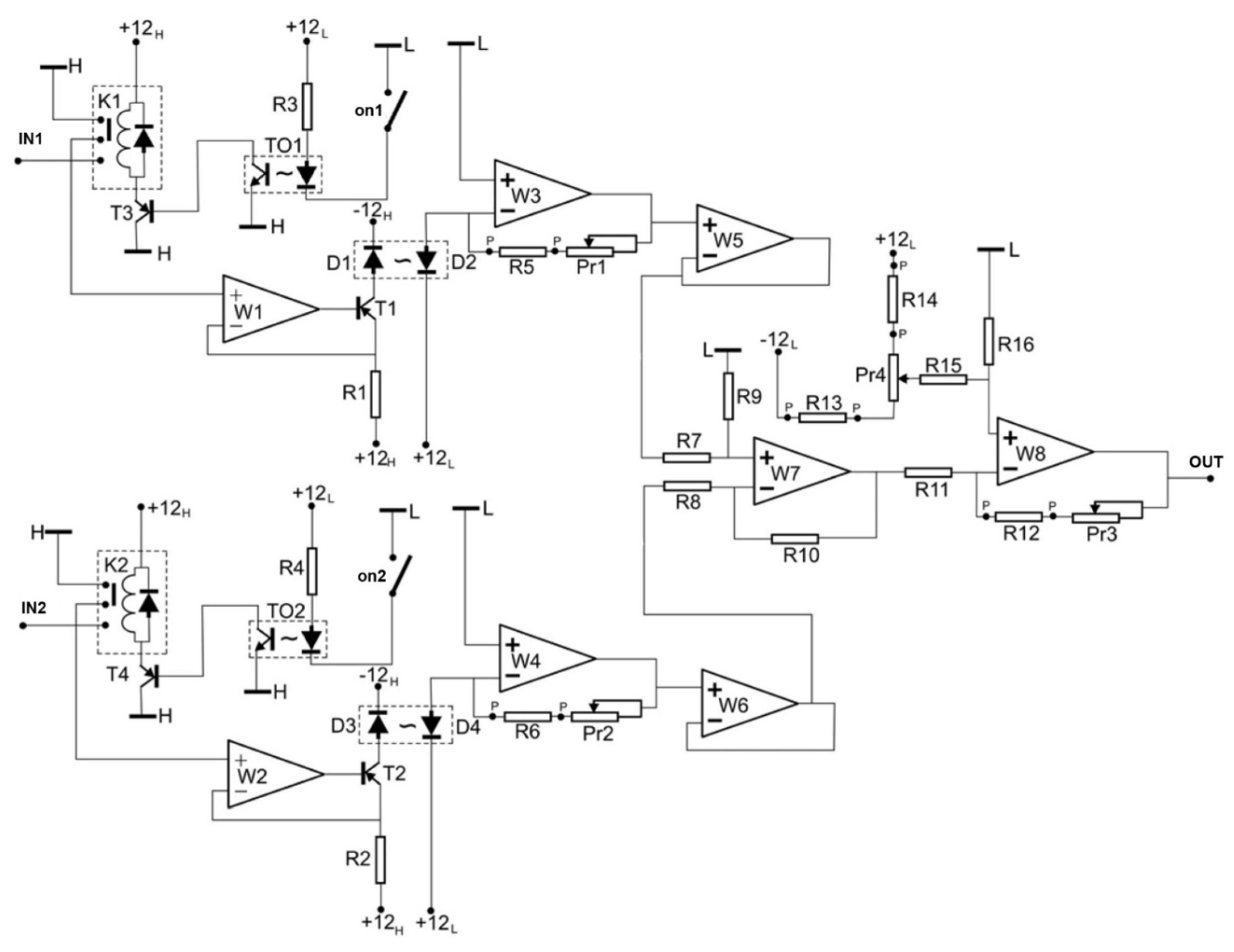
In
Figure 2 the internal diagram of the opto-isolation circuit designed to ensure high input impedance for measurements of the differential voltage is presented.
In
Figure 2 the following abbreviations are used:
+/−12H—positive and negative high voltage side supply voltage,
+/−12L—positive and negative low voltage side supply voltage,
L—ground,
H—high voltage potential from common voltage divider,
K1/2—reed relay for activation of inputs IN1/2,
TO1/2—transoptors with above 1 kV separation voltage,
on1/2—microswitch to activate the inputs by the transoptors,
D1/3—transmitting diodes of the opto-coupler circuit,
D2/4—receiving diodes of the opto-coupler circuit,
OUT—output of the opto-isolation circuit,
W1:6—high impedance (1012 Ω DC) operational amplifiers,
W7/8—fast differential amplifiers,
T1:4—transistors,
R1:15—resistors,
Pr1:4—variable resistors.
The W1 and W2 amplifiers are powered by high voltage side power supply, other amplifiers are powered by the low voltage side power supply.
Transmitting and receiving diodes in pairs D1 and D2, D3 and D4 are mounted in a 2.5 cm long tube.
Resistors R1 and R2 are used to provide adequate power of the transmitting diode.
Resistors from R8 to R10 are used to set the zero offset of the differential operational amplifier W7.
Resistors R13, R14, R15, R16 and Pr4 constitute the offset voltage compensation circuit.
Resistors R11, R12 and Pr3 set the gain of the entire path to the required value equal to 1.
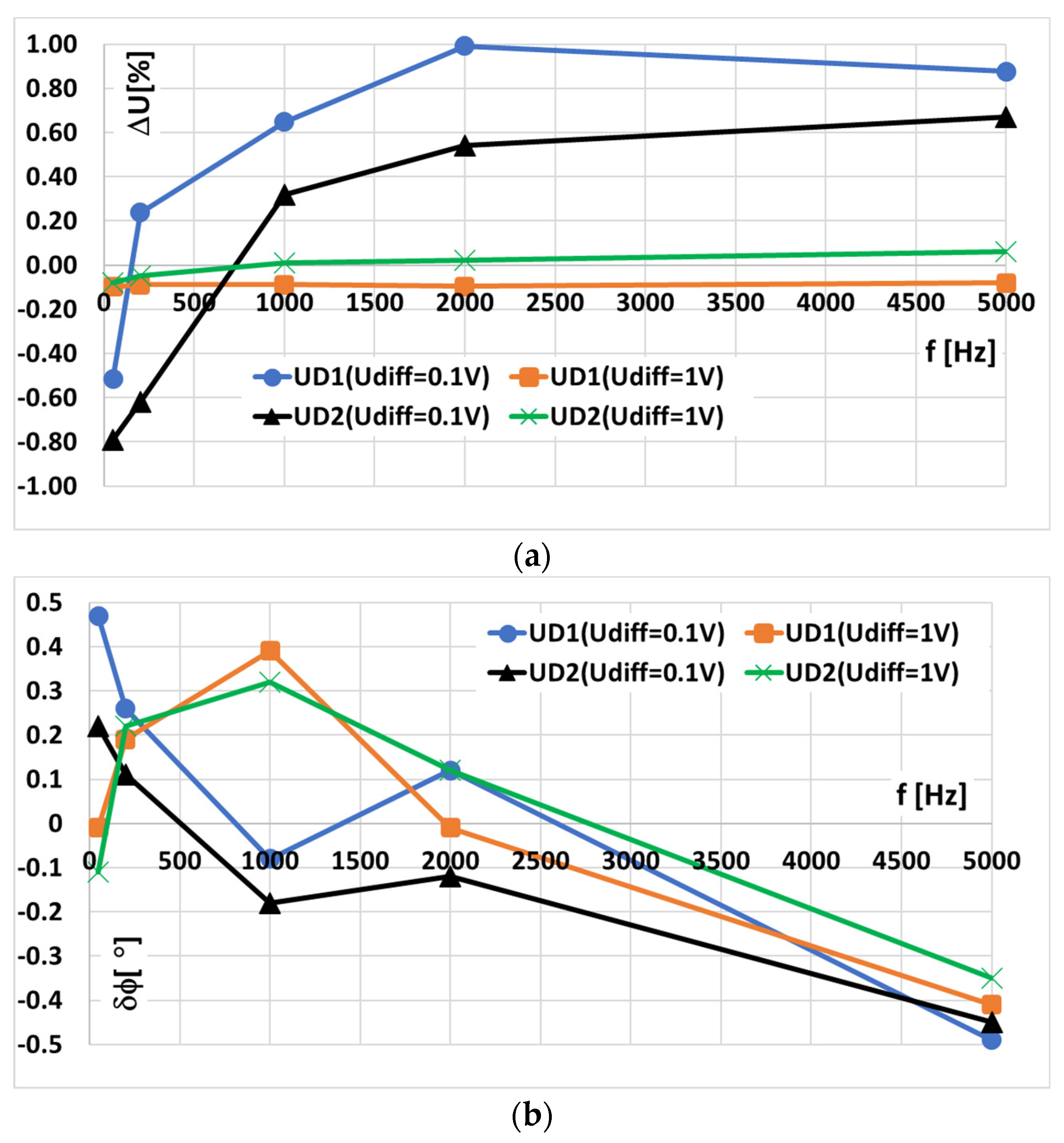
In
Figure 3a,b the results of the tests of the 1st and the 2nd units of the designed opto-isolation circuits performed to determine the RMS values of the internal noise for a given RMS value of the common voltage at frequency from 50 Hz to 5 kHz are presented.
The opto-isolation circuit is tested for the internal noise at various levels of common voltage and its frequency. In these conditions the differential inputs and the common voltage input are shorted together while the common voltage is applied. The output voltage is measured. In the ideal circuit the value should be equal to 0. The values of the output voltage are the same for both tested units. If the value of the common voltages are equal to 1 V or 10 V RMS, the output voltage is constant at level 1.5 mV RMS. If the value of the common voltage increases to 100 V RMS, the value of the output voltage increases with a frequency from 1.7 mV RMS for 50 Hz up to 5 mV RMS for 5 kHz. The measured value of the output voltage results not only from the different RMS values of the internal noise at each internal opto-isolation channel but also from its phase angle between the differential inputs of the internal operational amplifier W7.
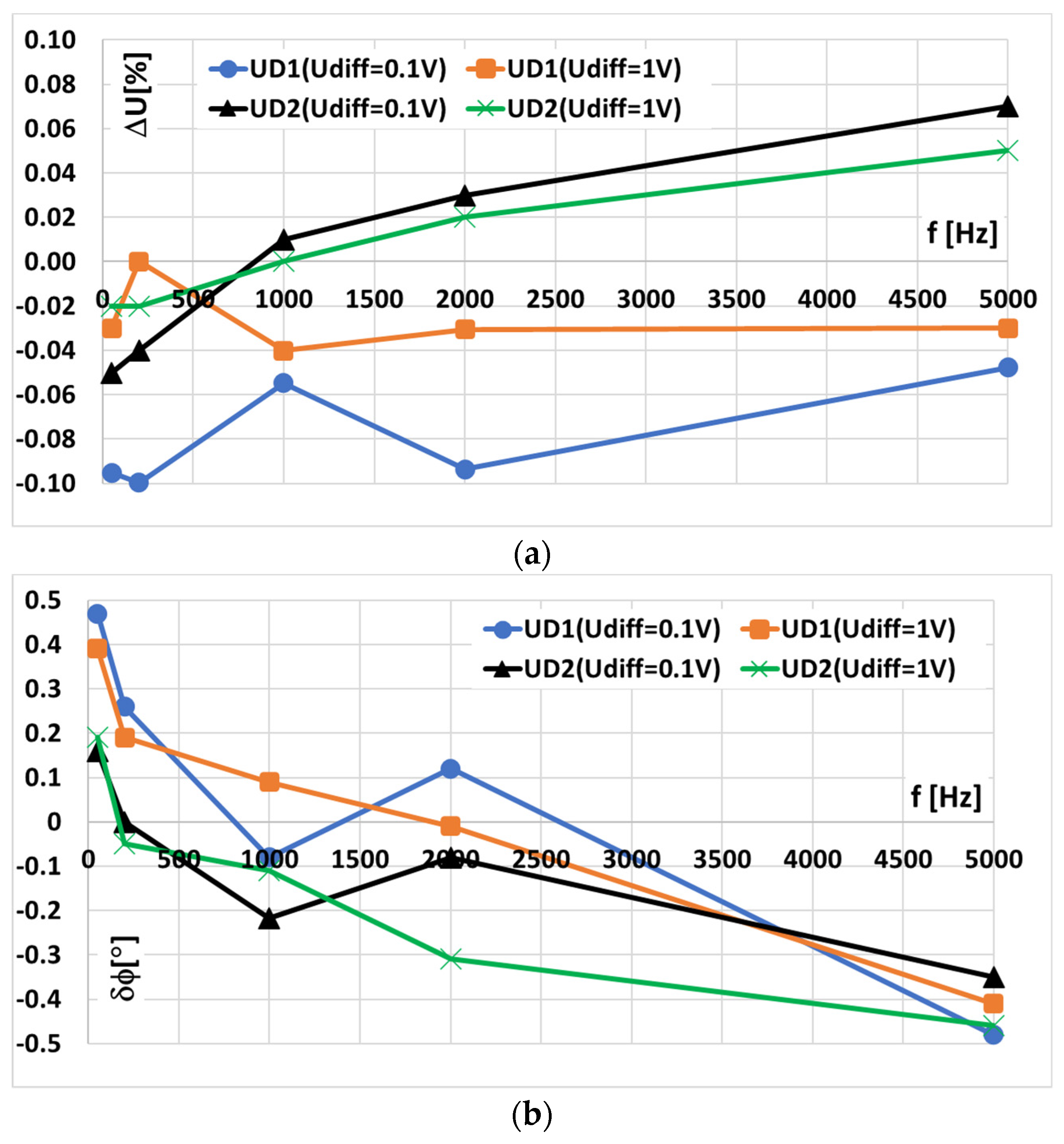
In
Figure 4a,b the results of the tests of the 1st and the 2nd units of the designed opto-isolation circuits performed to determine the calibration of the zero output voltage vs frequency of the differential input voltage at various levels of common voltage are presented.
The opto-isolation circuit is tested for the calibration of the zero output voltage at various levels of common voltage and its frequency. In these conditions the differential inputs are shorted together while the common voltage and input voltage are applied. The output voltage is measured. In the ideal circuit the value should be still equal to 0 since the differential voltage is equal to 0. The values of the output voltage are similar for both tested units. If the values of the common voltages are equal to 1 V or 10 V RMS, the output voltage is constant at level 1.7 mV RMS or 2.0 mV RMS. If the value of the common voltage increases to 100 V RMS, the value of the output voltage increases with a frequency from 2.2 mV RMS or 2.5 mV RMS for 50 Hz up to about 4.5 mV RMS for 5 kHz. The measured value of the output voltage in these conditions is similar to that obtained during the test of the internal noise. Therefore, the calibration of the zero value of the output voltage for zero value of the differential input voltage is performed correctly.
In
Figure 5a,b the 1st and the 2nd opto-isolation circuits’ conversion ratio errors under operation with an additional common voltage divider are presented.
In these conditions in the measuring system from
Figure 1, three voltage dividers are used. The output voltages of the
VD1 and the
VD2 are used to supply the differential input, while the VDCOM is used to supply the common voltage input. Therefore, the differential voltage between inputs
IN1 and
IN2 is measured in relation to the common voltage at input COM. Both input channels are insulated by the high impedance operational amplifiers and opto-isolation circuit of the coupling diodes.
The values of the opto-isolation circuits’ conversion ratio errors are not exceeding ±1%, while the value of the differential voltage is equal to 0.1 V RMS. Increases in the input voltage to 1 V RMS cause an increase in the accuracy of both tested units of the opto-isolation circuits to ±0.1%. This is due to the fact that the opto-isolation circuits’ conversion ratio errors result from the RMS value and phase shift of the internal noise between its internal input channels. The 1st and the 2nd opto-isolation circuits’ conversion phase error under operation with an additional common voltage divider are not exceeding ±0.5°, while the value of the differential voltage is equal to 0.1 V RMS and 1 V RMS.
In
Figure 6a,b the 1st and the 2nd opto-isolation circuits’ conversion ratio errors under operation without an additional common voltage divider are presented. If a single channel is required to ensure high impedance, one input is shorted with the common voltage input, while the other input is connected to the reference voltage divider. In these conditions in the measuring system from
Figure 1, two voltage dividers are used. The output voltages of the
VD1 are used to supply the differential input, while the
VDCOM is used to supply the common voltage input. Therefore, the differential voltage between inputs
IN1 and
IN2 (
COM) is measured in relation to the common voltage at input
IN2 (
COM). Only the
IN1 input channel is insulated by the high impedance operational amplifiers and opto-isolation circuit of the coupling diodes.
The values of the opto-isolation circuits’ conversion ratio errors are not exceeding ±0.1%, while the value of the differential voltage is equal to 0.1 V RMS and 1 V RMS. This is due to the fact that the opto-isolation circuits’ conversion ratio errors result from the RMS value of the internal noise of the single internal input channel. The 1st and the 2nd opto-isolation circuits’ conversion phase error under operation with an additional common voltage divider are not exceeding ±0.5°, while the value of the differential voltage is equal to 0.1 V RMS and 1 V RMS.
3. Applications of the Two Channel Opto-Isolation Circuit
In this paragraph of the paper, the application of the opto-isolation circuit to determine the values of the composite error of the tested voltage divider with the rated voltage ratios equal to 15 kV:100 V, 10 kV:100 V, 5 kV:100 V is presented. The opto-isolation circuit operates with an additional common voltage divider connected to the input
COM. The input
IN1 is connected to the high potential terminal of the output of the reference voltage divider. The input
IN2 is connected to the high potential terminal of the tested voltage divider (
Figure 7).
SVT—step-up voltage transformer [
20],
TVD—tested voltage divider,
RVD—reference voltage divider,
CS—current sense channel of DPM (voltage input designed to connect current probe),
V—voltage channel of DPM.
In
Figure 7 the opto-isolation circuit (
OIC) is used to determine the values of the composite error of the tested voltage divider (
TVD) in relation to the reference voltage divider (
RVD).
The composite error of transformation of the
hk-order harmonic of the distorted voltage ∆
εTVDhk by the
TVD is calculated from the equation
URVDhk—the RMS values of a given harmonic in the output voltage of the RVD,
UOIChk—the RMS values of a given higher harmonic in the output voltage of the OIC.
In accordance with analysis presented in papers [
14,
15,
19,
20], to decrease the measurement uncertainty of values of voltage ratio error and phase displacement, a hk harmonic of the output voltage
UTVDhk of
TVD may be calculated from the differential voltage measured by the
OIC.
φRVDOIC—the phase angle of a given harmonic in the output voltage of the OIC in relation to the same frequency harmonic in the reference voltage from the RVD.
The voltage ratio error (presented in (%)) of transformation of the
hk-order harmonic of the distorted voltage by
TVD is given by the equation
The phase displacement (presented in (°)) of transformation of the
hk-order harmonic of the distorted voltage by
TVD is given by the equation
In
Figure 8a,b the determined values of the voltage ratio error and phase displacement of the tested voltage divider at three ranges are presented.
The result of the measurements show that at the range 15 kV:100 V of
TVD the values of voltage ratio error and phase displacement did not exceed ±8% and ±9°, respectively. The result indicates that at the range 10 kV:100 V the values of voltage ratio error and phase displacement did not exceed ±5% and ±6°, respectively, while, at the range 5 kV:100 V the values of voltage ratio error and phase displacement did not exceed ±1.5% and ±1°, respectively. The advantage of the application of
OIC in testing the VDs is that it always ensure lower values of the measurement uncertainty than typical two channel systems, where reference voltage and output voltage of the tested VD are compared. The increase in the frequency of the measured voltage results in more significant differences between the measurement uncertainties, showing a higher advantage of the differential method. The measurement uncertainties of the voltage ratio error and phase displacement for two harmonics of frequency 50 Hz and 5 kHz, and their values 5.0% and 5.0°, are equal to [
20]:
- →
50 Hz: ±0.507%/±0.535°;
- →
5 kHz: ±0.178%/±2.160°.
The expanded combined measurement uncertainty for 5 kHz is about three-fold lower than for 50 Hz because the measured value of the voltage’s main component at the output of the RVD is ten-fold higher than the higher harmonic.
If the differential system is used with the designed
OIC, the expanded combined measurement uncertainties of the values of ratio error and phase displacement are equal to [
20]:
- →
50 Hz: ±0.015%/±0.013°;
- →
5 kHz: ±0.071%/±0.137°.
Therefore, the application of OIC to determine the values of the voltage ratio error and phase displacement for the transformation of distorted voltage harmonics enables decreases in the measurement uncertainty.
In the next paragraph the application of the opto-isolation circuit (
OIC) to determine the values of the composite error of the inductive VT with a voltage ratio equal to (15 kV/√3)/(100 V/√3) is presented. The
OIC operates without an additional common voltage divider. The input
IN1 is connected to the high potential terminal of the output of the reference voltage divider with voltage ratio equal to 15 kV/100 V. The input
IN2 is shorted with the common voltage input where the high potential terminal of the tested VT secondary winding is connected. The blocks diagram of the measuring setup is presented in
Figure 9.
TVT—tested voltage transformer,
ZL—load impedance of TVT (if required for test).
The composite error of transformation of the
hk-order harmonic of the distorted voltage by the TVT ∆
εTVThk is calculated from the equation
The
hk harmonic of the secondary voltage of TVT
UTVThk may be calculated from the differential voltage measured by the
OIC.
The voltage ratio error of transformation of the
hk-order harmonic of the distorted voltage by TVT is given by the equation
The phase displacement of transformation of the
hk-order harmonic of the distorted voltage by TVT is given by the equation
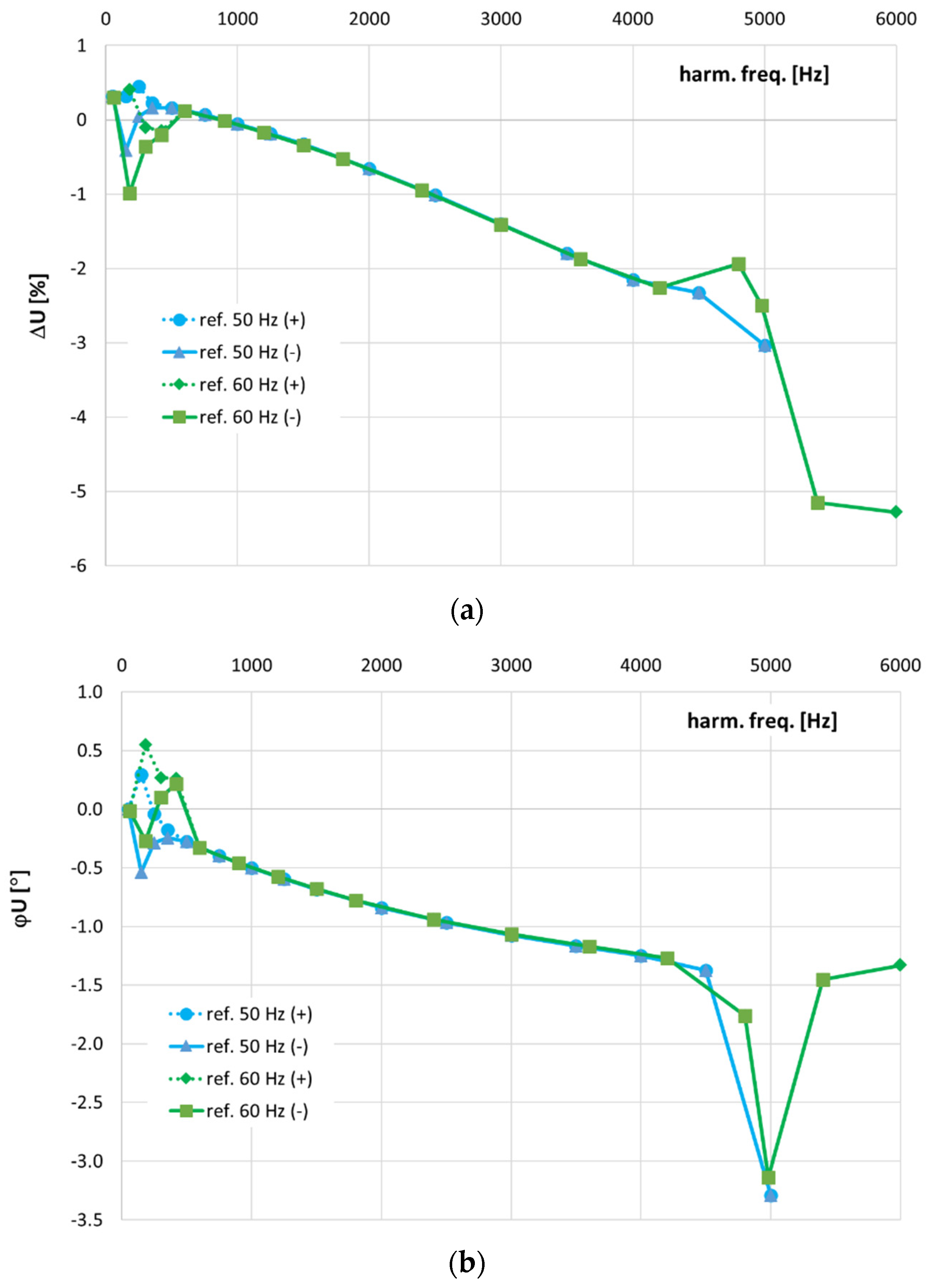
In
Figure 10a,b the determined values of the voltage ratio error and phase displacement of the tested voltage transformer (15 kV/√3)/(100 V/√3) are presented.
In
Figure 10 the following abbreviations are used
“50 Hz (+)” and “50 Hz (−)”—these plots present the results of the VT’s transformation accuracy of a given harmonic with the main component of frequency 50 Hz.
“60 Hz (+)” and “60 Hz (−)”—these plots present the results of the VT’s transformation accuracy of a given harmonic with the main component of frequency 60 Hz.
(+)—this notation means that the maximum positive values of voltage error and phase displacement are determined
(−)—this notation means that the maximum negative values of voltage error and phase displacement are determined.
The difference between the maximum positive values and the maximum negative values of voltage error and phase displacement results from the nonlinear of the B(H) curve of the tested inductive VT magnetic core and the self-generation of low-order higher harmonics to its secondary voltage [
4,
20,
24,
25]. Therefore, these curves are different only for the low-order higher harmonics up to about 500 Hz. The results of the measurements show that the values of the voltage ratio error and phase displacement of TVT did not exceed ±6% and ±3.5°, respectively. These values significantly increase with the frequency of transformed higher harmonics. This is caused by the increase in the reactance of the winding of TVT and the increase in their voltage. At a frequency of about 5 kHz, a resonance is detected causing a rapid increase in the VT’s voltage error and phase displacement [
26,
27,
28].
If the differential system with the designed OIC is used, or a typical two channel system where output voltages of TVT and RVD are measured, the expanded combined measurement uncertainties of the values of ratio error and phase displacement are equal to those determined for TVD in the previous analyzed case. The advantage of the application of OIC in testing the VTs is still that it ensures lower values of the measurement uncertainty than the two channel system.


