1. Introduction
Dual active bridge (DAB) topology is among the most popular DC/DC converters used in electronic power systems. This topology is widely used in DC/DC microgrids as well as mixed networks and owes its popularity to many advanced features such as bidirectional power flow, galvanic isolation, control simplicity, wide range of voltage regulation, and soft switching of semiconductor devices. DAB topology has been applied to solid-state transformers, electromobility, energy storage systems, and DC voltage distribution networks [
1,
2]. Nowadays, the development of DAB converters is mainly focused on the increase in energy efficiency by using modern power semiconductors (SiC, GaN), where the adaptation of new control strategies enables a reduction in the current stress and the limitation of current RMS values, and a diminishing of DAB transformer power losses [
1,
2,
3,
4,
5,
6]. Crucially, the application of modern power semiconductor devices enables an increase in the switching frequency up to 1 MHz [
7], which results in a higher power density, a reduction in passive components dimensions, and a reduction in the overall converter dimensions.
The problem of energy efficiency evaluation is one of the main aspects of the beginning stage of the design process of a future converter. Importantly, a proper evaluation of power losses allows for a selection of cooling methods and radiator features, which reduce the overall converter dimensions and the total cost. At the early stages of the design process, energy efficiency may be estimated using a simulation tool or via an analytical analysis. Many simulators (e.g., PLECS) offer comprehensive tools for the evaluation of power losses and a thermal analysis using electro-thermal models [
8]. This method is easy to use and delivers results with a satisfactory accuracy for the design purpose. However, it requires access to precise models of semiconductors, which not all suppliers offer, because such models are usually shared by manufacturers only for selected types of semiconductors, or the developed models are dedicated to one specific simulator. Crucially, many models of semiconductors presented in the literature cannot be parameterized using the manufacturer’s datasheet, hence additional laboratory measurements are required to obtain the model parameters, which is usually time-consuming and increases the total cost [
9,
10].
Notably, the measurement of some quantities in the DAB converter (e.g., the power loss of a transformer) may be problematic, hence using analytical methods may be a suitable approach to obtaining a power loss distribution.
Another approach uses an analytical analysis based on a set-up of mathematical equations describing the function of the considered converter. It is worth mentioning that the presence of high-frequency currents in a DAB converter AC circuit, or the determination of the switching process mechanism of semiconductors (under soft or hard conditions) in dependence on the converter AC side currents values results in limited usefulness of the analytical methods, which have been derived for classic H-bridge topologies. These approaches are usually described for sinusoidal modulation with a low fundamental current frequency at the inverter AC side [
11,
12,
13]. Moreover, in some systems, the transistor turn-on losses are neglected [
14], or it is assumed that both the turn-on and turn-off processes perform only under hard switching conditions [
12]. In available application notes, switching losses under hard conditions are usually calculated using simplified formulas with constant values of time parameters describing the switching processes [
4]. Moreover, to simplify the considerations, the impact of transistor gate resistance is often omitted [
12,
14,
15].
In the literature, analytical methods of power loss estimation dedicated to DAB converters have also been proposed.
For example, in [
16], an analysis of a power transfer in a single-phase DAB converter was provided. The presented analyses were performed for different cases of input-to-output voltage relations including the influence of the dead time and conduction losses of semiconductor devices. However, the presented analysis was incomplete as it omitted the discussion of the impact of semiconductor switching losses and transformer losses. An interesting approach was presented in [
17], where a theoretical analysis of power losses was given, which was used for the optimal design methodology of a single-phase DAB converter. A valuable part of this work is a presentation of an estimation method of capacitors and transformer losses. The obtained results were compared with the results of the simulation and experimental measurements to prove the correctness of the adopted methodology, however, an analysis of the semiconductor switching losses was not included—the authors assumed that all switches were switched under soft conditions. Another solution was presented in [
18], where an analysis of the conducted differential mode current harmonic magnitudes and the power factor in a DAB converter was discussed. Importantly, that solution was based on a Fourier series theory, hence its adaptation is more complex and time consuming. This approach may be used for the overall prediction of the DAB operational performance and to optimize and identify the current and voltage ranges. Commutation losses were not considered here either; hence based on the methodology presented in [
18], the DAB converter efficiency may only be evaluated in a generic way.
The approach presented in [
19] was dedicated to the estimation of semiconductor losses including the impact of dead-time and turn-off process for SiC MOSFET and Si IGBT transistors operating in DAB converters. All of the required parameters may be easily extracted using the manufacturer’s datasheet. The used mathematical expressions are not complicated, and method adaptation is not time-consuming. It should be noted that the presented considerations did not take into account the transformer losses, which is a significant disadvantage of the method.
A more advanced approach was described in [
20], where the estimation method of semiconductors and transformer losses was proposed. The obtained results were used to improve the overall energy efficiency by modifying and optimizing the DAB converter control strategy. The limitations of the primary approach are the omission of the diodes’ reverse recovery process and neglect of the impact of transistor gate resistance on the switching process dynamics.
A comprehensive estimation method of the DAB converter efficiency was proposed in [
21]. The transformer losses were predicted using the Steinmetz equation and the semiconductors’ conduction and switching losses were also calculated. Additional analyses were performed for hard and soft switching conditions in dependency on the current values in the AC circuit of the DAB converter. The high accuracy of the obtained results and the usefulness of the proposed approach were confirmed by a comparison with the experimental measurement results. However, two different polynomial functions—one for hard switching and one for soft switching—must be used to calculate the semiconductor switching losses. Parameters of these functions were fitted by using least means squares approximation. As a result, the method is complicated and time-consuming.
Based on the presented analysis, it appears that a different approach is necessary. In this paper, a calculation method of power loss and energy efficiency of a one-phase DAB converter composed with SiC-MOSFETs and controlled with single phase shift was proposed. The proposed set of equations, whose coefficients may be easily obtained from the manufacturer’s datasheets, describes the commutation and conduction losses of diodes and transistors and the transformer losses were also considered. The correctness of theoretical considerations was verified by comparing the analytical results with the experimental ones, performed on a 5 kW DAB converter prototype.
3. Currents Estimation in a DAB Converter
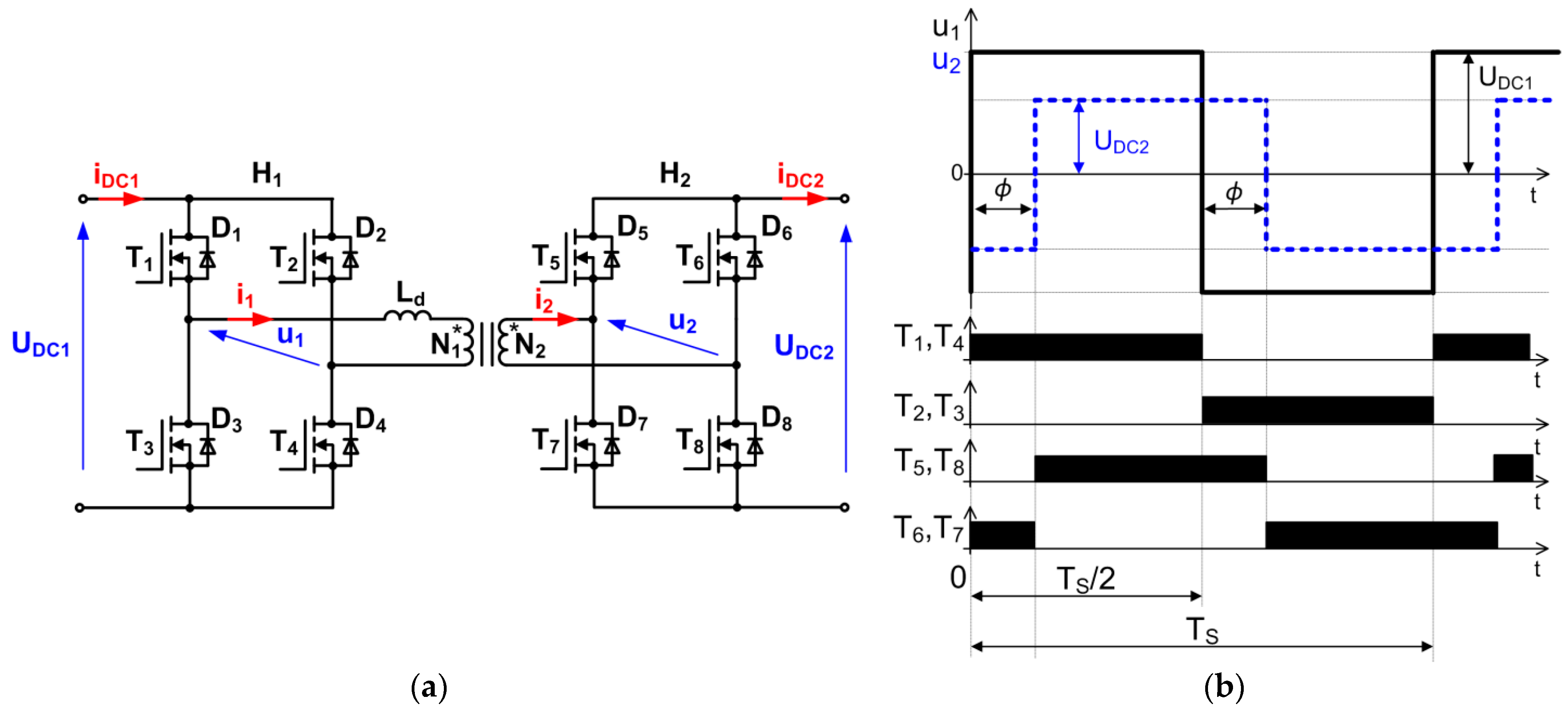
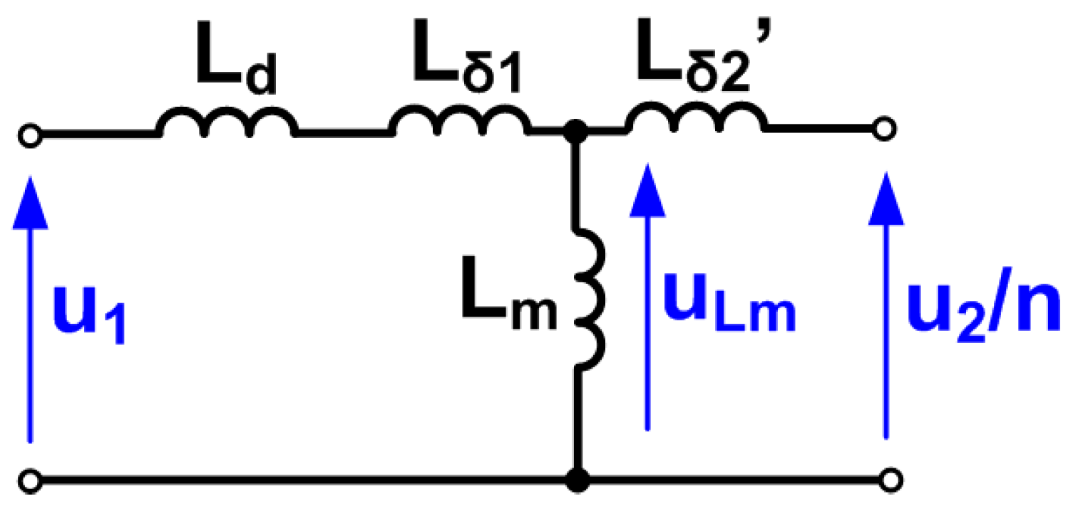
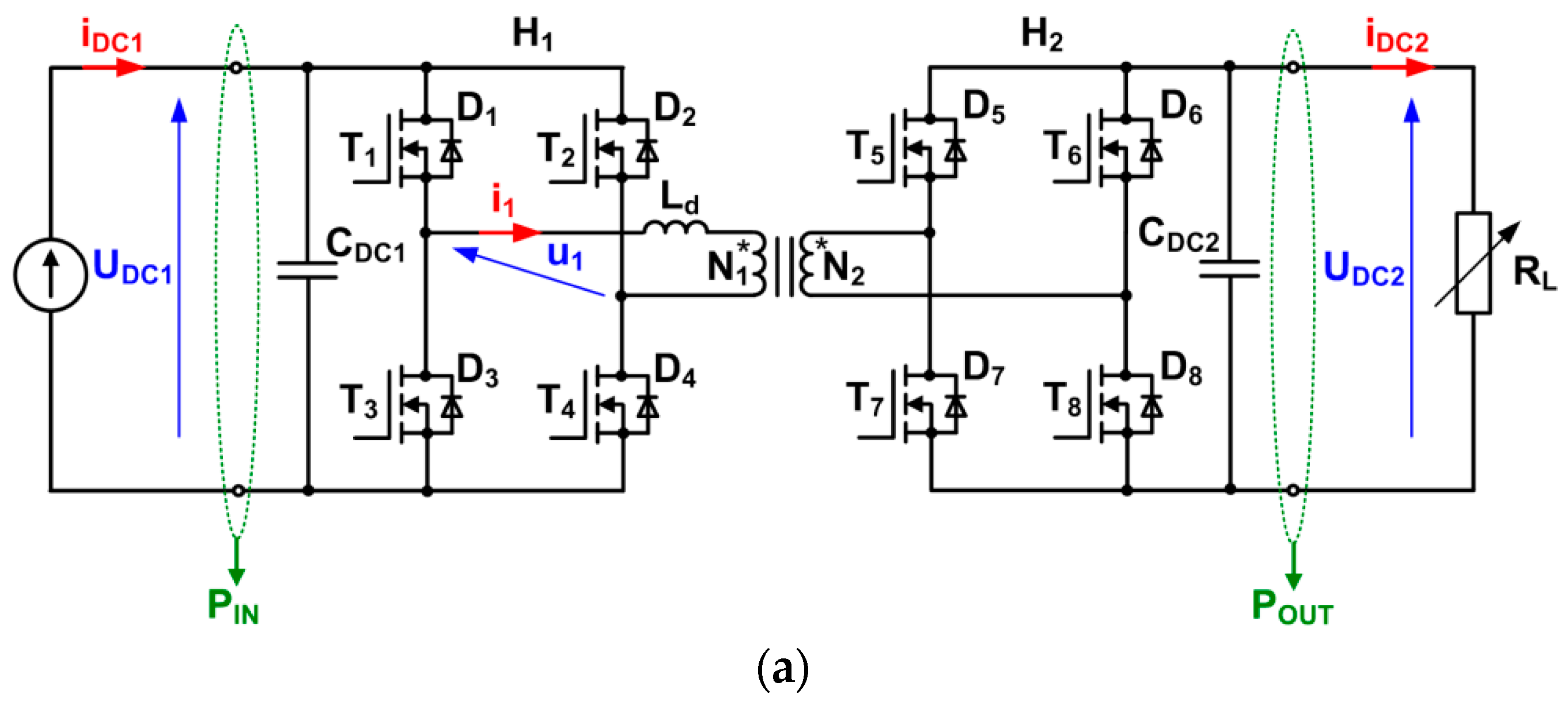
An equivalent circuit of the single-phase DAB converter (
Figure 1a) is presented in
Figure 2. A resultant inductance
L represents a sum of inductances in the AC-circuit:
where:
- -
Ld—inductance of the additional inductor;
- -
Lδ1, Lδ2′—leakage inductance of each transformer winding converted to the bridge H1 side: Lδ2′ = Lδ2/n2;
- -
Lδ2—leakage inductance of transformer winding at the H2 bridge side;
n = N2/N1—transformer turns ratio.
In the presented equivalent scheme, values of the H2 bridge voltages and currents are also referred to the H1 bridge side.
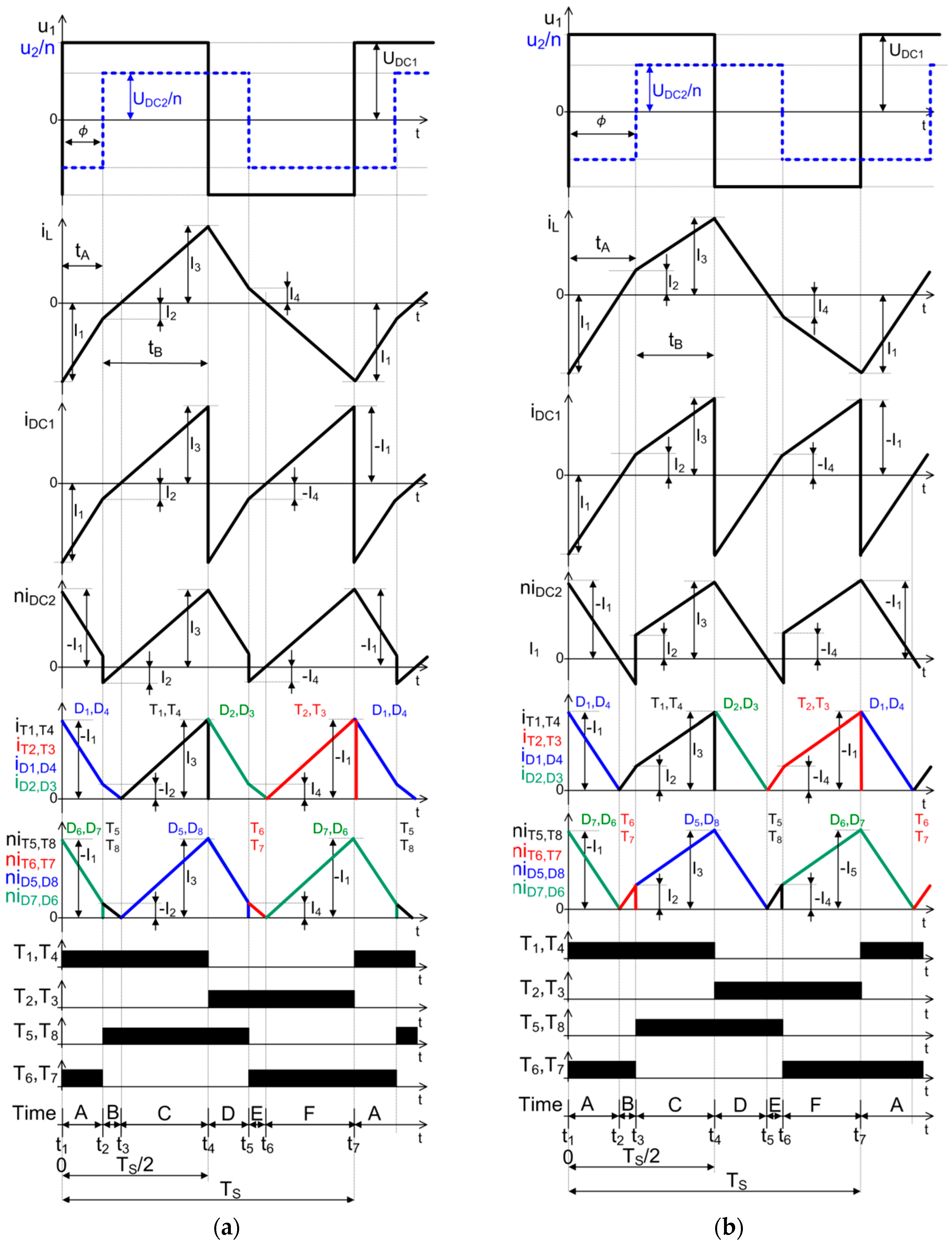
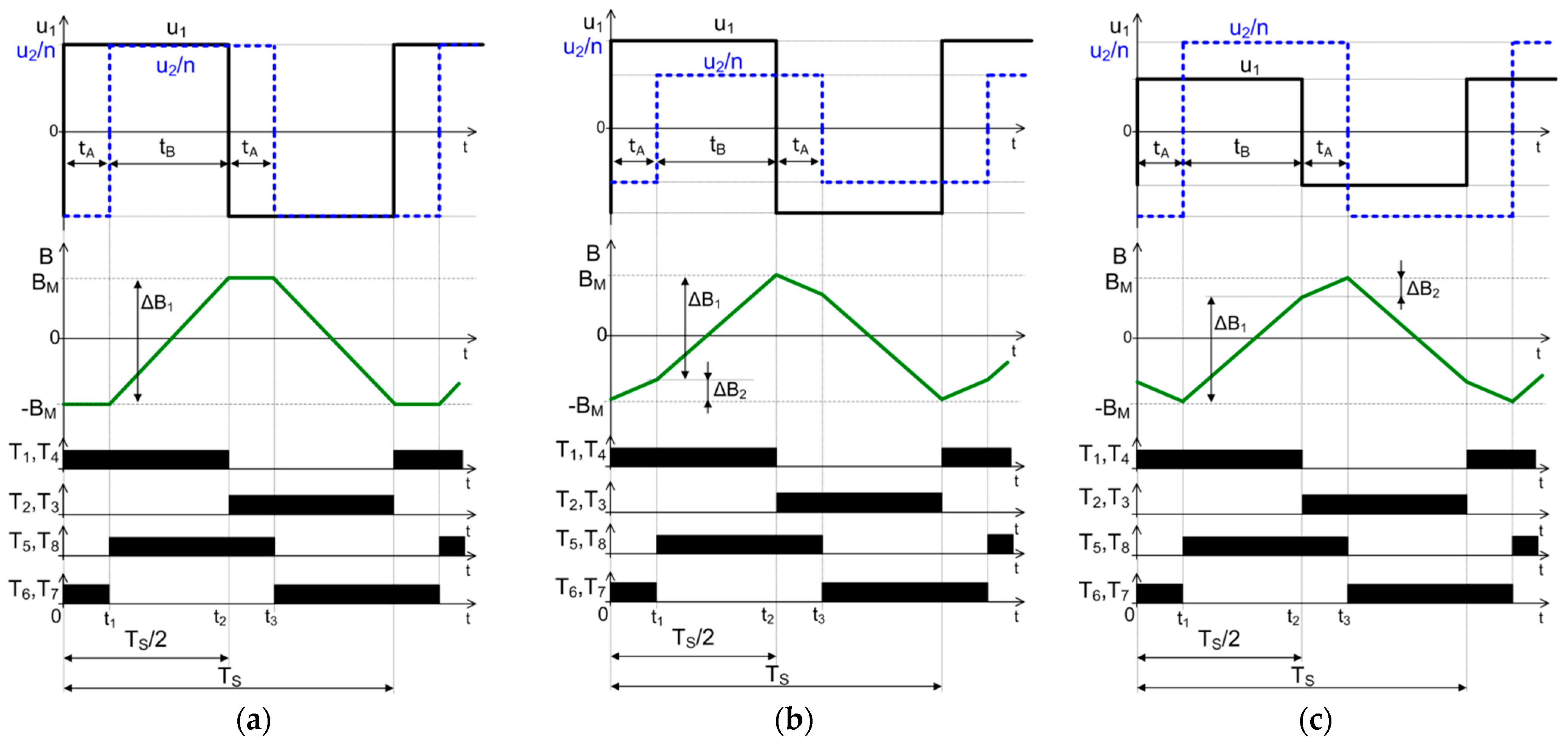
In this study, the DAB converter features were considered when the SPS modulation strategy was applied. Each bridge generated a quasi-square wave voltage
u1 and
u2/
n with a 50% duty cycle (
Figure 3).
The value and power flow direction between bridges
H1 and
H2 are controlled by the phase shift
ϕ. To simplify the calculations, the impact of the transistors’ dead time may be neglected. Similarly, it can be assumed that the values of voltages
UDC1 and
UDC2/
n are high enough, which enables the voltage drop to be omitted at the transistors and diodes. In brief, positive values of the phase shift are used when
UDC1 >
UDC2/
n, however, for a negative value of
ϕ, the results may be obtained using a similar approach. In
Figure 4, exemplary theoretical waveforms are presented, when
UDC1 <
UDC2/
n and
ϕ > 0.
Based on
Figure 3a and an equivalent scheme of the DAB converter (
Figure 2), voltage
uL, affecting the inductances in the AC-link, is described by:
- -
for the time interval
tA:
- -
for the time interval
tB:
Hence, the current
iL in specified time moments is described by:
and
Thus, the average values of the input and output currents
IDC1 and
IDC2 are given by:
and
Because
tA = TS/2
− tB and substitutions (2) and (3) to (8), (9) leads to:
and
For known values of IDC1(av) or IDC2(av), n and UDC1 or UDC2, the length of the time interval tB may be easily extracted by solving Equations (9) or (10). Next, the length of interval tA may be obtained for a specified switching time TS, which allows for a calculation of the values of current iL at characteristic moments of the DAB converter operating cycle.
4. Estimation of Transistor and Diode Power Losses
The total power loss
PT of a single transistor operating in a H-bridge is the sum of commutation losses and conduction loss
PC(T):
where
PON(T) and
POFF(T) are the turn-on and turn-off switching losses, also called the commutation losses. The total power loss of a single diode
PD may be defined in an analogous way.
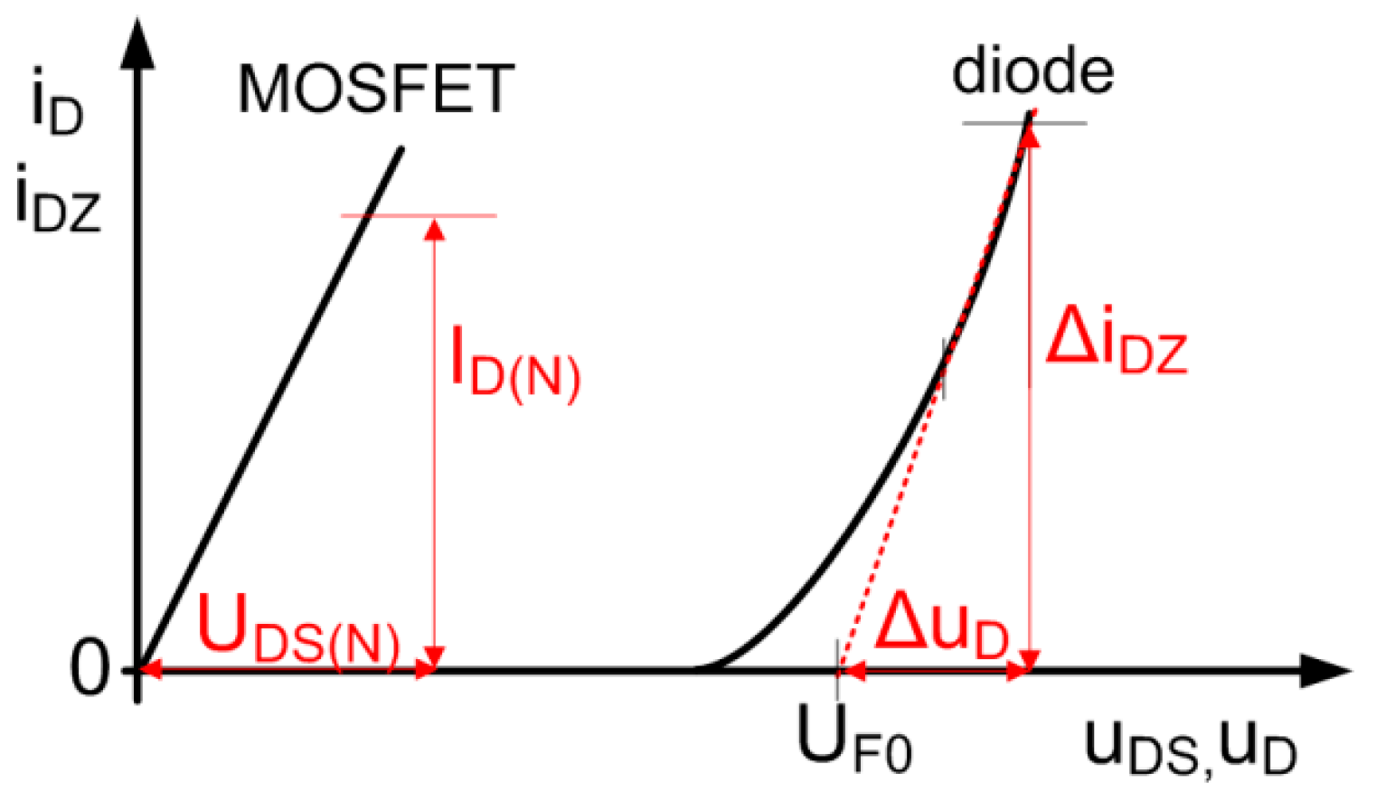
Conduction losses result from voltage drops on conducting transistors and diodes. If MOSFET transistors are applied in a converter construction, using a linear approximation of the transistor output characteristic
iD(
uDS) (
Figure 5) allows one to estimate a voltage drop
uDS depending on a drain current
iD:
where
UDS(N) and
ID(N) are the rated values of the transistor drain-to-source voltage
uDS and drain current
iD (given in the manufacturer’s datasheet).
Similarly, using a linear approximation of the datasheet diode characteristic
iDZ(
uD), the voltage drop
uD caused by a flow of current
iDZ may be calculated as:
where
UFO is a diode threshold voltage and
rD is the diode dynamic resistance
rD = Δ
uD/Δ
iDZ (
Figure 5).
Hence, the conduction power loss of the MOSFET transistor and diode calculated for one switching period TS are given as follows:
- -
- -
and for the diode:
where
ID(rms) and
IDZ(rms) are rms values of transistor and diode currents and
IDZ(av) is an average value of a diode current
iDZ calculated for one switching period
TS.
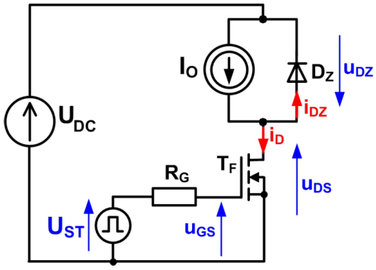
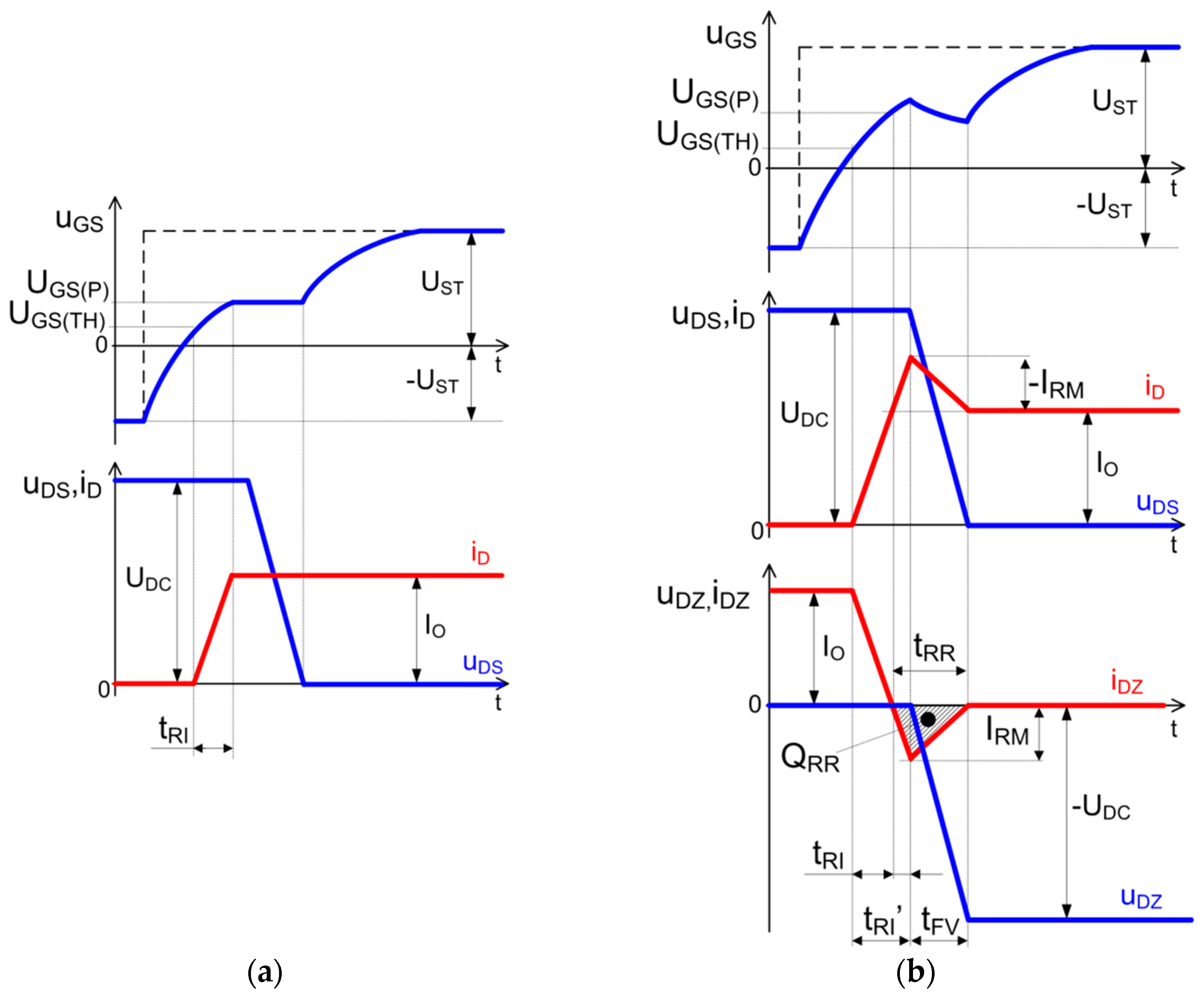
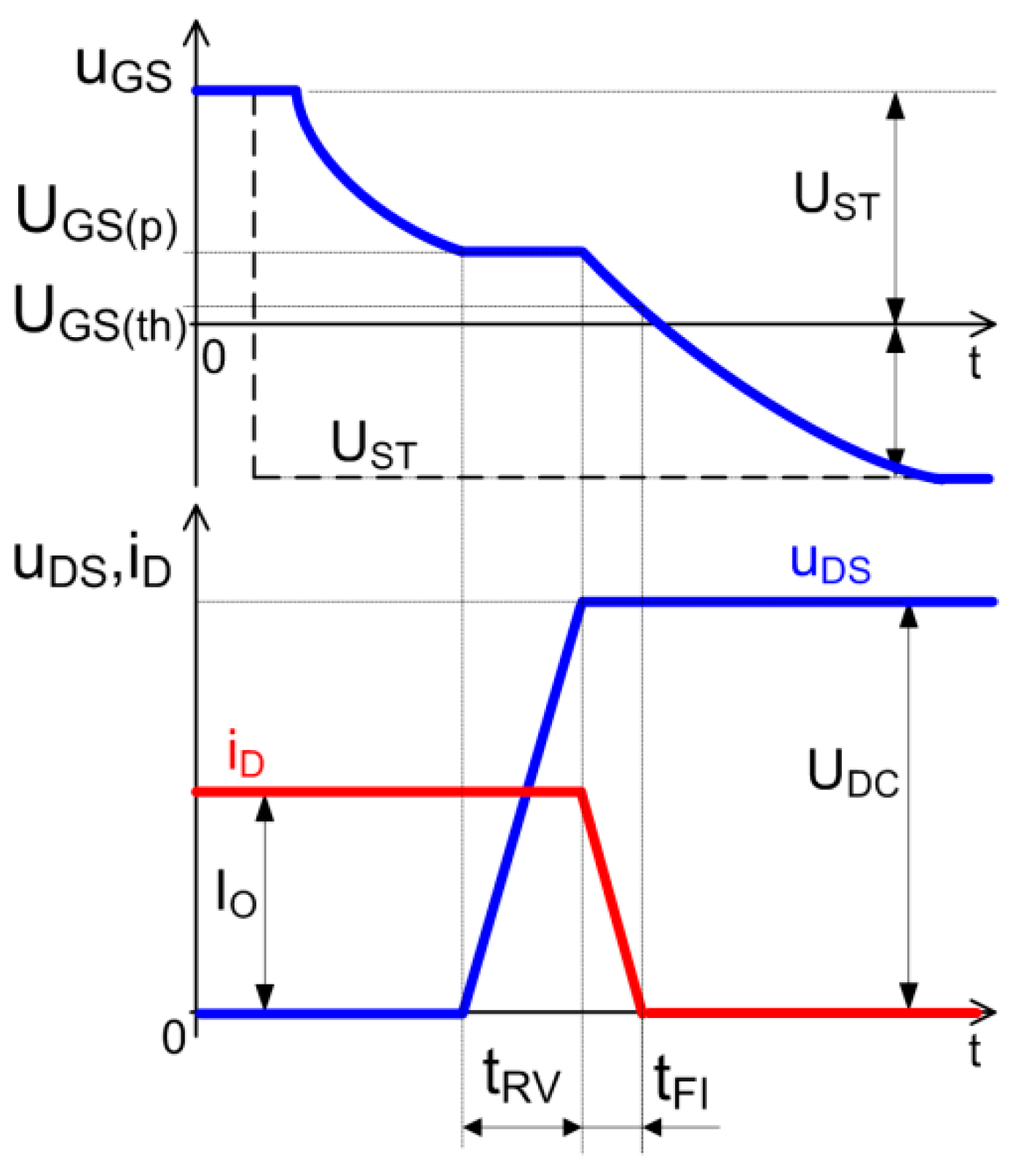
Commutation losses result from finite values of the rise and fall times of the transistor voltage and current waveforms during switching processes. Considering the theoretical voltages and current waveforms obtained in a basic switching cell (
Figure 6) during the transistor turn-on process under hard conditions, the transistor current
iD reaches the value of the load current
IO before the reduction in the drain-to-source voltage
uDS [
26] (
Figure 7).
Hence, in the turn-on process of a transistor, two characteristic sub periods may be described. Impacted by the diode
DZ reverse recovery, during the first stage of the turn-on process, the drain current rises to the value, which is a sum of the absolute values of load current
IO and reverse recovery current
IRM of diode
DZ (
Figure 7b). Considering the waveforms presented in
Figure 6, the transistor current
iD derivative with time is expressed by:
To estimate the current
iD rise time
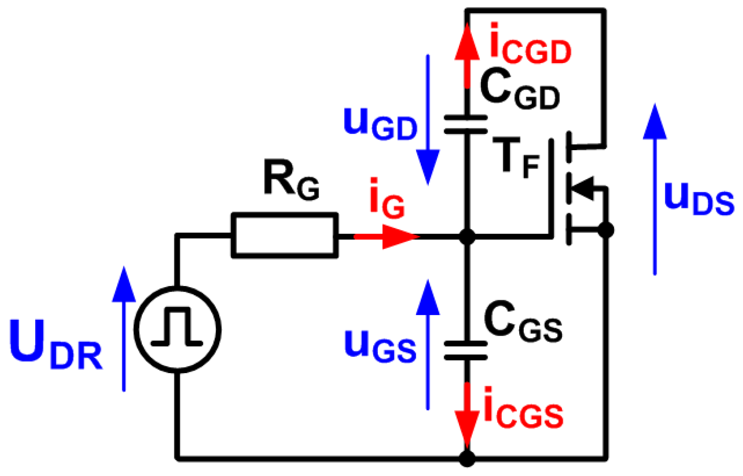
tRI, a MOSFET gate circuit should be analyzed (
Figure 8). During the transistor switching process, which is caused by drive voltage
UDR changes, transistor parasitic capacitances
CGD and
CGS are recharged by the gate current
iG [
27]:
The gate current
iG may also be described by the equation:
where
RG is an external gate resistance. In the manufacturer’s datasheet, the values of capacitances
CGD and
CGS are given as an input capacitance
Ciss and a reverse transfer capacitance
Crss with the following relationships:
and
Next, substituting (18)–(20) to Equation (17):
which leads to:
During the current
iD rise phase of the turn-on process, to simplify the calculations, it can be assumed that the voltage
uDS remains constant and its derivative with time equals zero (
Figure 7). Hence, Equation (22) may be modified as follows:
Next, transforming Equation (23):
the rise time
tRI is given by:
where
UGS(TH) is a MOSFET gate threshold voltage and
UGS(P) is a minimal value of the gate-to-source voltage, enabling the conduction of the load current
IO. These values may be obtained from a datasheet transfer characteristic
iD(
uGS). After the calculation of parameter
tRI, the value of derivative
diD/
dt may be easily estimated using (16).
To estimate the diode turn-off power loss under hard-switching conditions, a reverse-recovery process must be used. Hence, the values of reverse current
IRM and diode reverse recovery time
tRR should be evaluated (
Figure 7b). To solve this problem, a number of analytical methods using datasheet information have been proposed. For example, in [
28], a regression method was proposed to obtain the reverse-recovery parameters during switching intervals, and in [
29], a set of equations including, additionally, the impact of parasitic inductances and diode capacitance, was proposed. These methods offer satisfactory accuracy with a maximum error of parameter estimation lower than 10%, however, their application seems to be complex and time consuming. Considering the waveforms presented in
Figure 7b, the values of parameters
tRR,
IRM, and
QRR depend on the load current
IO, diode current derivative with time
aiDz, and temperature [
30]. In this paper, to be concise, the effect of temperature was omitted. Based on the results of the measurements and the manufacturer’s data, the following empirical relations enabling the estimation of
tRR and
IRM for various values of load current
IO and
aiDZ = diDZ/
dt were derived:
and:
where:
- -
aiDZ = diDZ/
dt =
−aiD (from Equation (16) and
Figure 7b);
- -
tRR(N) is a nominal value of the diode DZ reverse recovery time measured for the nominal load current IO(N) and nominal derivative with time of the diode current AiDZ(N). These nominal values are usually given in the manufacturer’s datasheet.
Thus, the total length of interval
tRI′ (
Figure 7b) is given by:
When the transistor drain current reaches the maximum value, the next phase of the turn-on process begins. Voltage
uDS starts to fall and, by the end of interval
tFV, the recombination process of the diode charge is finished—voltage
uDS is reduced to zero and the diode current is zero (
Figure 7b) [
12]. Factually, at that moment, the diode current was limited to about 10% of
IRM and the voltage
uDS was reduced to the value resulting from the voltage drop on the conducting transistor. Hence, the transistor voltage fall time
tFV is described by:
Considering the waveforms presented in
Figure 7b and based on the estimated values of
tRI′ and
tFV, the turn-on power loss of the MOSFET
PON(T) under hard switching conditions is expressed by:
which leads to:
Similarly, the diode reverse recovery power loss is given by:
During the MOSFET turn-off process under hard conditions, the transistor
uDS voltage reaches the value of the supply voltage
UDC before a reduction in the drain current
iD (
Figure 9) [
26,
31]. Analyzing the MOSFET turn-off process (
Figure 9), two characteristic phases may be recognized:
- -
during time interval tRV, voltage uDC rises to UDC;
- -
during time interval tFI, drain current iD decreases do zero.
During time interval
tRV, assuming the gate-to-source voltage
uGS is constant, the transistor is turned off within the flat Miller Plateau Region. Because
uGS = UGS(P) and
duGS/
dt = 0, Equation (22) may be simplified:
which leads to:
The relation describing a current
iD fall time may also be derived in an analogous way:
Thus, MOSFET turn-off power losses are given by:
For example, from
Figure 3, it can be distinguished that transistor pair
T1 and
T4 in bridge
H1 is switched on when diodes
D1 and
D4 conduct, which forms soft switching conditions. Similarly, the turn-on process of transistors
T2 and
T3 also occurs under ZCS (zero current switching) conditions. Hence, it can be assumed that the turn-on power loss for these transistor pairs
PON(T) = 0. At moments
t4 and
t7, transistor pairs
T1,
T4 and
T2,
T3 are switched off. In this study, the least favorable operating conditions of semiconductors were assumed, hence, to calculate the power loss
POFF(T) from Equation (36), it was assumed that transistor pairs
T1,
T4 and
T2,
T3 were turned off under hard-switching conditions with a current
iT1,T4(
t4)
= iT2,T3(
t7)
= −I1 = I3 and supply voltage
UDC =
UDC1. From
Figure 3, it can also be distinguished, that if
I2 < 0, then transistors
T5,
T8 are switched on and diodes
D6,
D7 are turned off under hard-switching conditions. To calculate transistor
T5 turn-on power losses
PON(T5) and diode
D6 turn-off power losses
POFF(D6), Equations (31) and (32) should then be used for
UDC = UDC2 and
IO = I2/
n. The turn-off process of transistors
T5,
T8 occurs under ZCS conditions, hence, the commutation loss
POFF(T5) equals zero. If
I2 > 0, the transistor
T5,
T8 turn-on process ensues when diodes
D1,
D4 conduct, which allows for the development of soft-switching conditions. Nevertheless, the
H2 bridge transistors’ turn-off process occurs under hard switching conditions. To calculate the commutation power loss
POFF(T5), Equation (36) may be applied for
UDC =
UDC2 and
IO =
I2/
n. Notably, that power loss may be calculated only for one transistor and diode for each of bridges
H1 and
H2. Hence, the power loss of transistor
T1 is given by:
where the transistor
T1 conduction power loss
PC(T1) may be calculated from (14):
and
IT1(rms)2 is obtained by:
The commutation power loss
POFF(T1) is described in Equation (36). Because diode
D1 is turned off under soft-switching conditions, only a conduction loss (see Equation (15)) may be taken into account:
where
ID1(av) and
ID1(rms)2 are given as follows:
For the known values I1, I2, and I3, the length of the time intervals (t2 – t1), (t3 – t2), and (TS/2 – t3) for specific values of voltage UDC1 and UDC2/n may be obtained from modified Equations (4)–(6).
The total power losses of the
H1 bridge transistors is equal to:
and the total power losses for the bridge
H1 diodes are given by:
Hence, the total power losses of bridge
H1 is equal to:
The total power losses of all transistors (PTH2) and diodes (PDH2) in a H2 bridge may be obtained in an analogous way.
5. Transformer Losses
For the analytical evaluation, it was assumed that the transformer total power loss
PTR is a sum of the power loss in the core
PFE, and the power losses generated in the primary and secondary windings are
PCU(prim) and
PCU(sec).
To calculate the core power loss
PFE, a modified Steinmetz’s formula may be used, which for rectangular voltages is given as follows [
32,
33]:
- -
f—inducplified waveforms of voltages;
- -
BM—induction peak value [T];
- -
TC—core temperature [°C];
- -
VC—core volume [cm3].
The coefficients of Equation (50) may be directly obtained from datasheets developed by the core manufacturers.
Considering the scheme presented in
Figure 2, an equivalent circuit of the transformer connected in series with an additional choke placed at the primary side is shown in
Figure 10. Thus, a magnetizing voltage
uLm affecting the magnetizing inductance
Lm is described by:
From
Figure 2, neglecting a voltage drop on the diodes and transistors and assuming a rectangular shape of the voltage waveforms, the voltages
u1 and
u2/
n were equal to, respectively
, ±UDC1 and
±UDC2/
n. From (51), it may be distinguished that the worst working conditions of core occurred when
Ld = 0 and
Lδ2 =
Lδ2′. Hence, the magnetizing voltage
uLm is then given by:
and induction
BM reaches the maximum possible values. Based on waveforms presented in
Figure 11,
BM may be described in the following way:
- -
- -
- -
if
UDC1 <
UDC2/
n (
Figure 11c):
where
SC is a cross-sectional area of the core.
To simplify the estimation of the transformer windings’ power loss
PCU, calculations may be performed for the windings’ resistance measured for the switching frequency
fS = 1/
TS and the rms value of the windings’ currents according to the formula [
32]:
where
RCU(prim),
RCU(sec) are the resistances of the transformer windings (respectively at the
H1 bridge side and
H2 bridge side) measured for the switching frequency
fS;
I1(rms) is the rms value of the transformer current at the bridge
H1 side;
I2(rms) is the rms value of the transformer current at the bridge
H2 side given by:
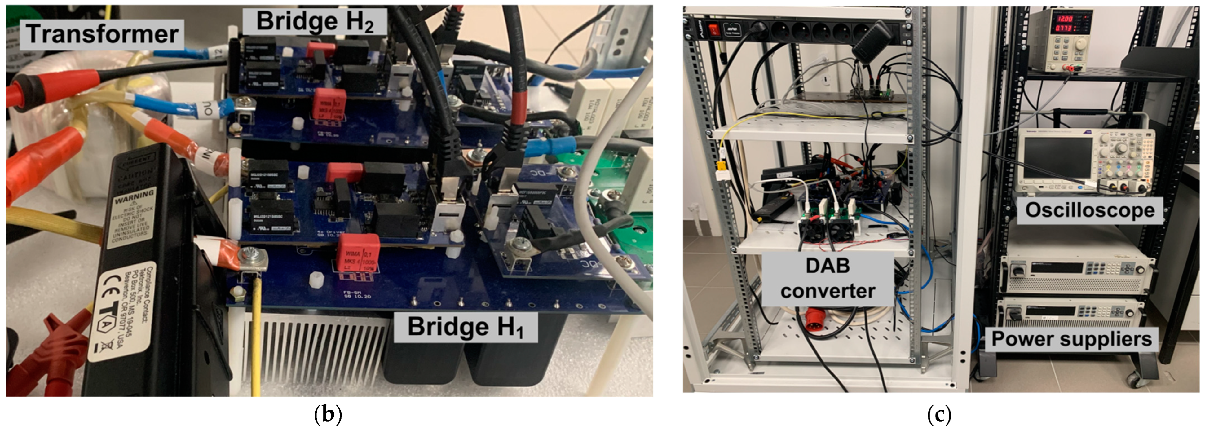
6. Validation
The parameters that are required for DAB converter efficiency calculation using the proposed approach were collated and are explained in
Table 1. The described approach was validated by a comparison of the estimated DAB efficiency characteristics with the experimental ones measured for the converter, whose parameters are shown in
Table 2. To measure the input
PIN and output
POUT power (
Figure 12) of the tested DAB converter, a Yokogawa WT5000 precision power analyzer was used. Importantly, the experimental measurements were performed for the DAB converter in a basic configuration without any additional sub-circuits (e.g., start-up resistors were disconnected). Voltages
UDC1 and
UDC2 were kept at a constant level
UDC1 = 670 V and
UDC2 = 385 V and the output
POUT power was controlled by changes in the load resistance
RL. In the applied laboratory conditions, the maximum output power was limited to 5 kW due to the limitation of the measurement range of the used power analyzer. Waveforms of the current
i1 and voltage
u1 in the AC circuit were measured using a Tektronix DPO3034 oscilloscope equipped with the high-voltage differential probe P5210A and the current probe TCP404XL.
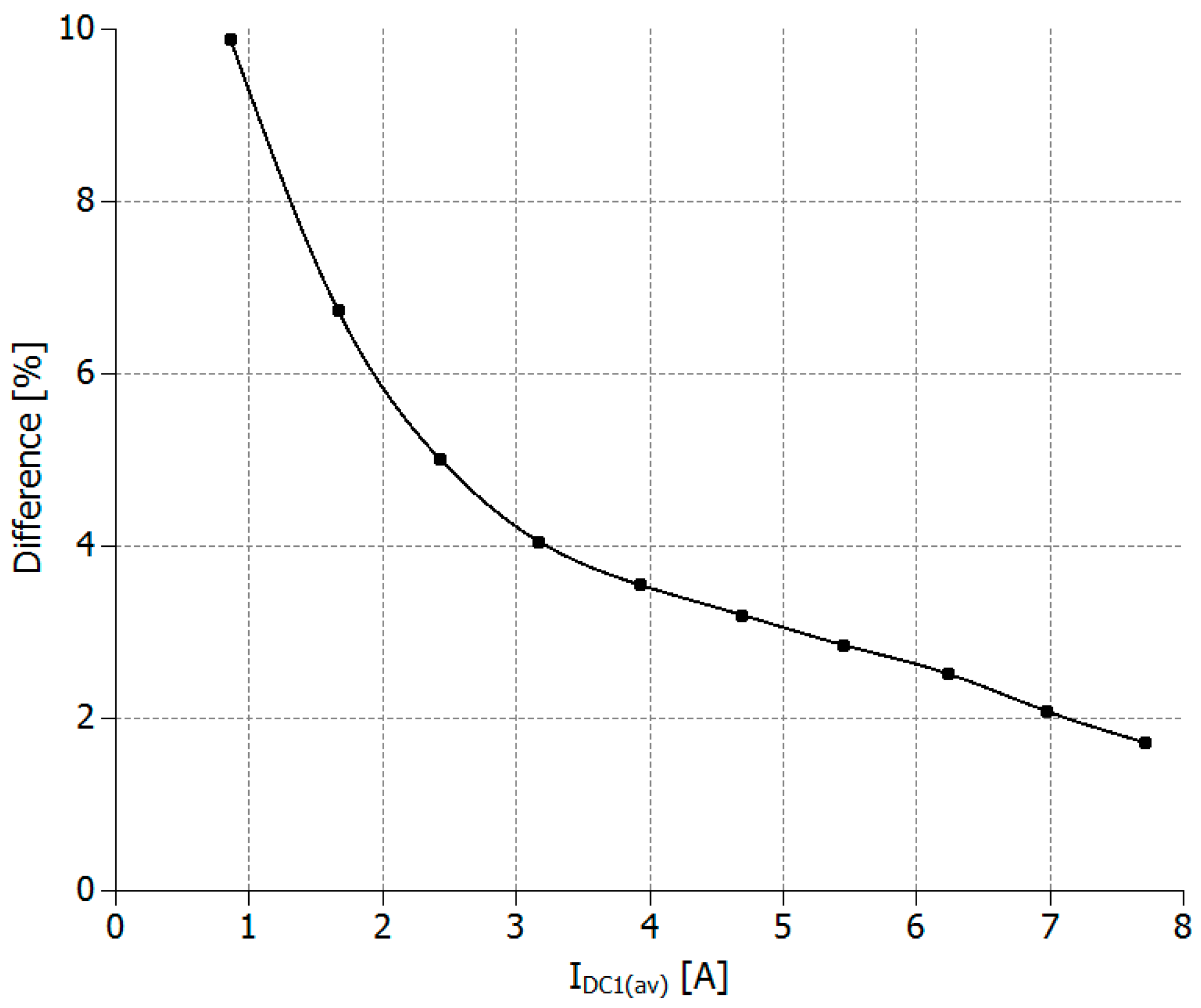
At the first step, the accuracy of the input current average value estimation
IDC1(av) was evaluated. For the known values of the output power
POUT and voltage
UDC2, based on Equations (7)–(10), the average value of the input current was calculated and compared with the experimental results. The maximum noted difference between the estimated and measured values did not exceed 10% and the accuracy increased with the growth in the output power and input current value (
Figure 13). Crucially, the proposed analytical approach was simplified, so the impact of some factors (e.g., time dead influence) was not factored in. As a result, the accuracy of the estimation at a lower level of load may be worse.
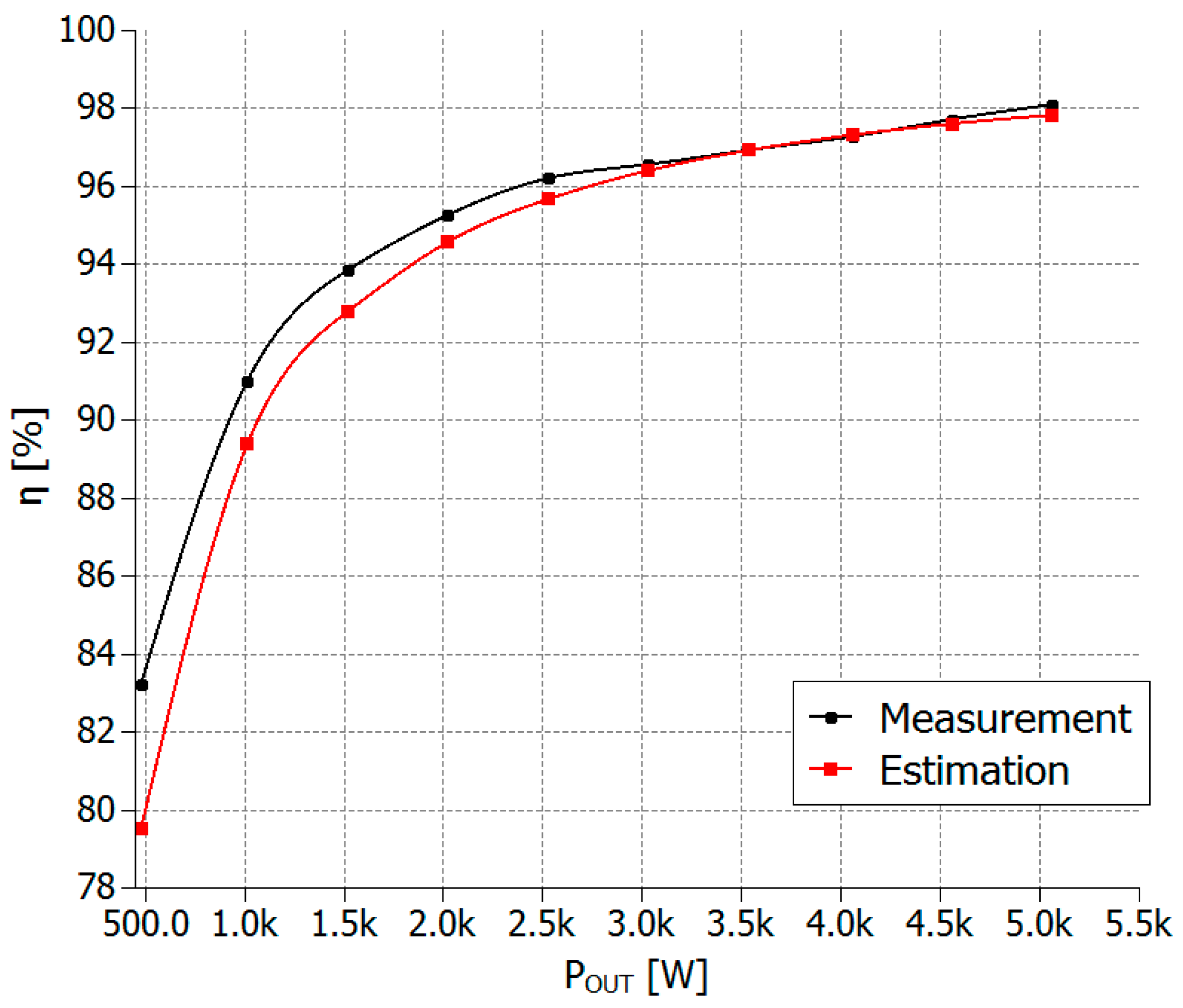
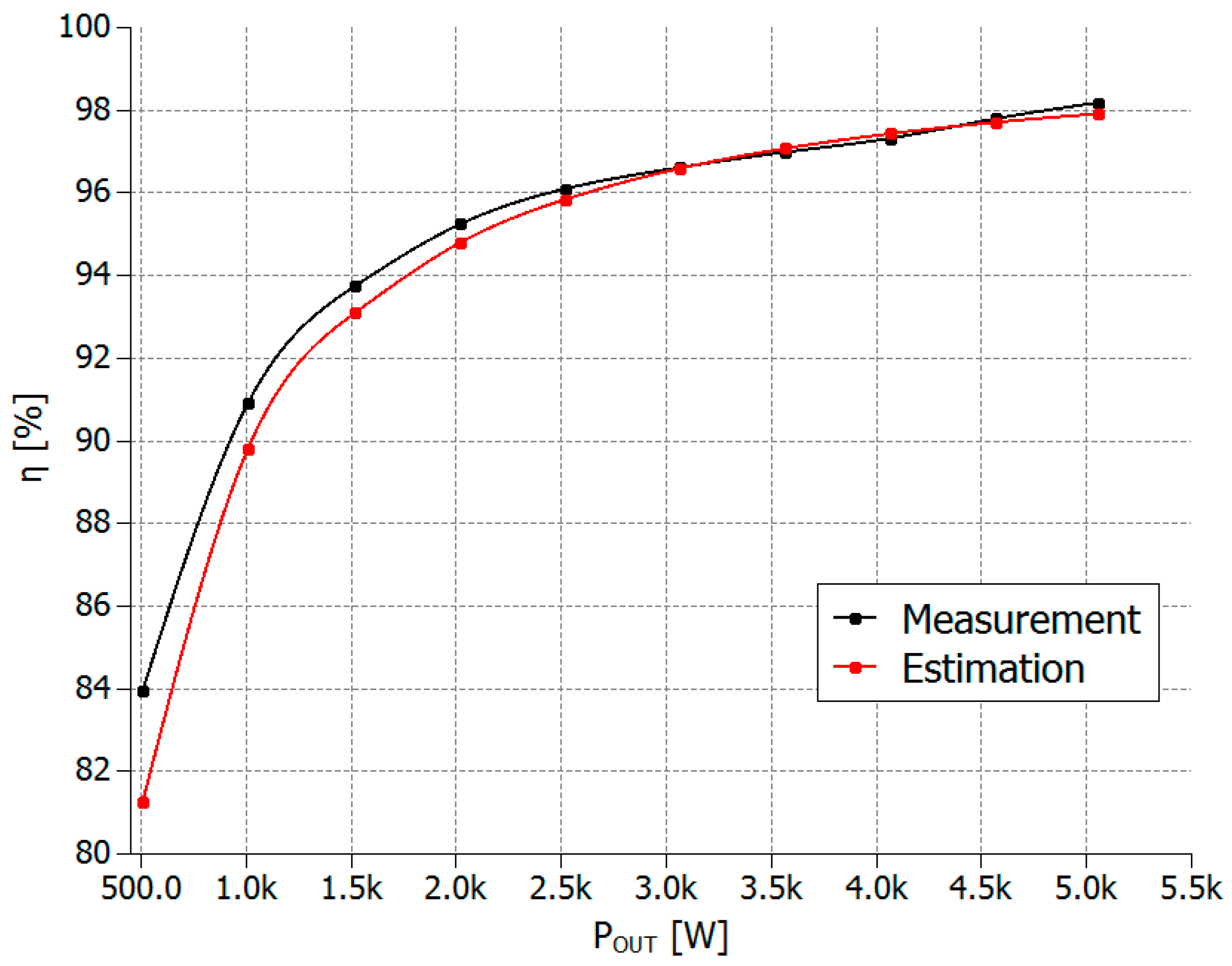
A similar conclusion may be drawn for the comparison of the DAB estimated and measured energy efficiency characteristics (
Figure 14). The estimated
η (
POUT) characteristic followed the shape of the measured one with the highest accuracy noted for the output power exceeding 50% of the maximum out-power. The maximum noted efficiency for the tested DAB converter in a specific range of output power up to 5 kW reached 98%, which was confirmed by both the experimental and analytical results.
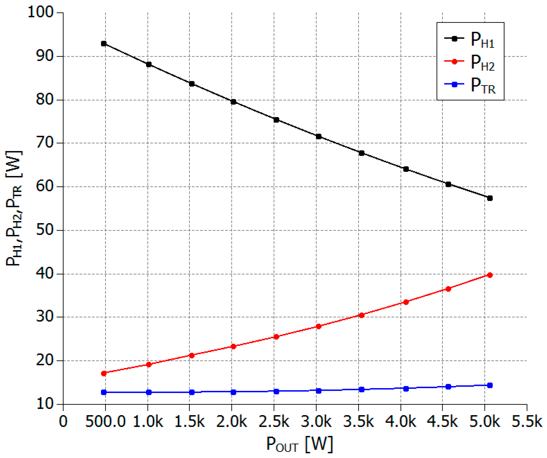
The application of the proposed analytical method enabled an estimation of the power loss distribution for the main converter components. Based on the estimated characteristics presented in
Figure 15, it can be stated that the power losses were mainly generated in bridges
H1 and
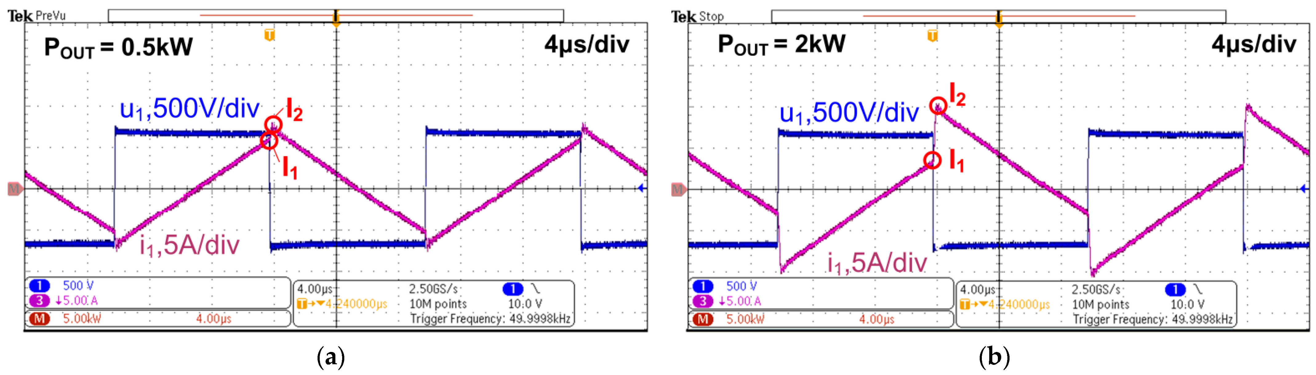
H2. Notably, the considered DAB converter operated in conditions that correlated with the theoretical current and voltage waveforms presented in
Figure 4a. As a result, transistors
T1–
T4 were turned on under hard-switching conditions with current
I1 > 0 and
I1 =
−I3. Thus, the commutation power losses in bridge
H1 resulted from the transistor’s turn-on process and the reverse recovery process of diodes
D1–
D4. Because value
I1 decreases with the growth of the DAB output power (
Figure 16), the commutation losses in bridge
H1 also decrease, so, as a consequence, the bridge
H1 total power loss
PH1 is reduced.
From
Figure 4a,
T5–
T8 were turned off under hard-switching conditions with the current determined by the value of
I2/
n = −
I4/
n. Similarly, since the
I2 value increased with the growth of the out-power
POUT (
Figure 16), the transistor’s commutation losses increased, so in bridge
H2, the total power loss
PH2 grew. From
Figure 15, the transformer loss
PTR obtained using Equation (49) was significantly lower than the losses noted for bridges
H1 and
H2.
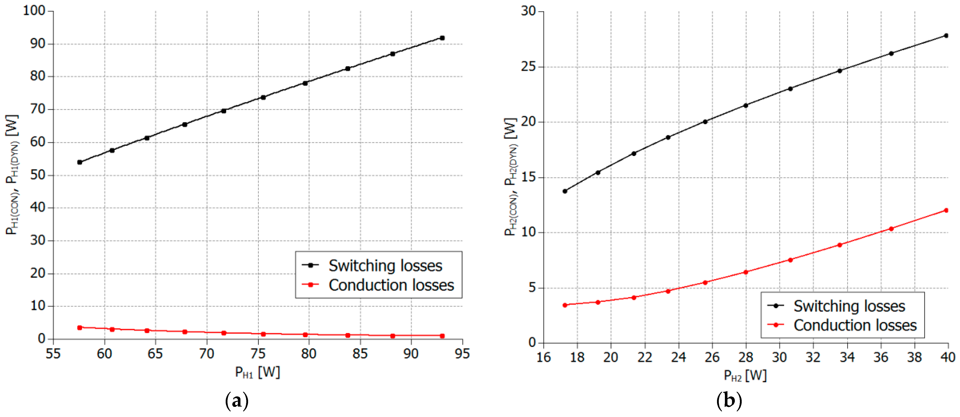
Losses generated in each of the bridges
H1 and
H2 were mainly determined by switching losses, however, the share of conduction losses increased with the growth in the DAB converter output power, which resulted from Equations (14) and (15) (
Figure 17).
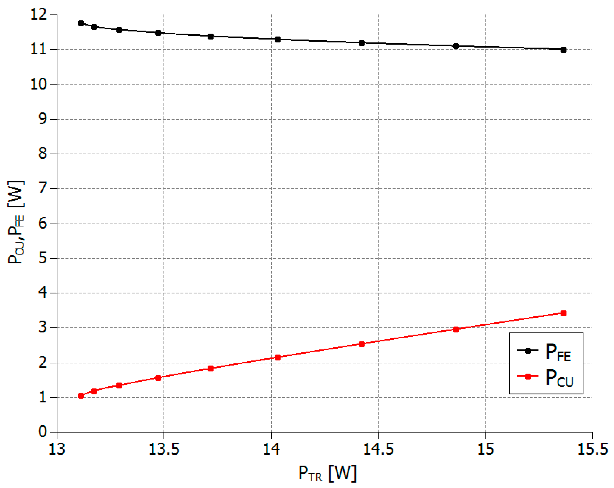
Based on the results of the analytical calculation, transformer losses
PTR are determined by the loss in the core
PFE (
Figure 18). In the tested DAB converter, for the specified range of output power up to 5 kW, the value
tB changed within a small range (coefficient
tB/(0.5
TS) does not fall below 0.95), hence, according to Equations (50)–(55), a slight reduction in the core loss
PFE was observed. The windings’ total power loss
PCU depends on the rms value of the primary and secondary windings currents, so it should grow with the increase in the DAB converter output power, which was confirmed by the results of the analytical calculations.
The presented calculations were also performed for the case when energy was transmitted from bridge
H2 to
H1. In this case, the obtained analytical characteristic
η(
POUT) was also confirmed by the results of the experimental measurements, which validated the adopted approach (
Figure 19). Moreover, the results of a detailed analysis of power loss distribution were also convergent with the description above.
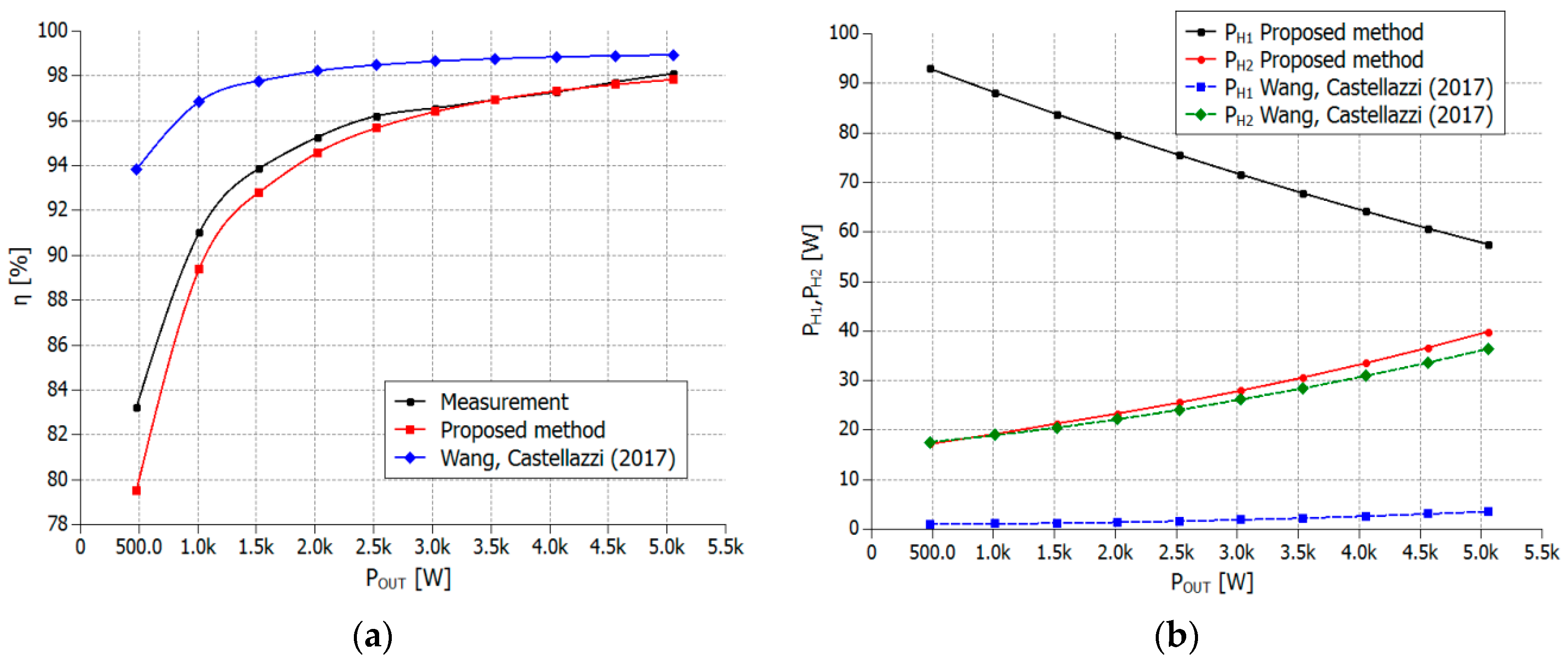
Obtained results were compared with ones calculated using the approach proposed in [
19]. Adapting this solution is not time-consuming, and all of the required parameters may be obtained based on the manufacturer’s datasheet. However, in [
19], no methods of transformer loss estimation were proposed, so in both approaches, the same setup of equations based on Steinmetz’s formula was used to evaluate the transformer losses. Using both of the compared methods, the obtained efficiency characteristics, calculated for the case when energy was transferred from bridge
H1 to
H2, are presented in
Figure 20a. Higher accuracy of the proposed solution was noted, especially for the light load of the converter. At higher loads, the predominance of the proposed method was also distinguishable. However, the difference between the measured and estimated results using the approach in [
19] decreased with the growth in the output power
POUT. One of the main assumptions of the method in [
19] is that all transistors are switched-on under soft conditions. It should be noted that considering the assumed direction of energy flow, the transistors in bridge
H1 are turned on under hard-switching conditions. As a result of the transistors’ turn-on power losses omission, the total losses of bridge
H1 were underestimated, as presented in
Figure 20b. Both compared methods enabled the estimation of the transistors’ turn-off losses. However, to simplify the calculations, in the method [
19], constant values of the current fall time were assumed. For the converter light load, the obtained power losses of bridge
H2 were comparable. However, the difference between the calculated results slightly increased with the growth in the output power
POUT.


 ,
, 


