Article

A Step-Up Converter with Large Voltage Gain and Low Voltage Rating on Capacitors

by
Miguel Ramirez-Carrillo
1,
Susana Ortega-Cisneros
1,
Julio C. Rosas-Caro
2,*,
Jorge Rivera
1,
Jesus E. Valdez-Resendiz
3,*,
Jonathan C. Mayo-Maldonado
4,* and
Antonio Valderrabano-Gonzalez
2,*
1
Department of Electronic System Design, Centro de Investigación y de Estudios Avanzados del Instituto Politécnico Nacional, Zapopan 45017, Jalisco, Mexico
2
Facultad de Ingeniería, Universidad Panamericana, Alvaro del Portillo 49, Zapopan 45010, Jalisco, Mexico
3
Tecnologico de Monterrey, Avenida Eugenio Garza Sada 2501, Monterrey 64849, Nuevo Leon, Mexico
4
Department of Electronic and Electrical Engineering, The University of Sheffield, Sheffield S10 2TN, UK
*
Authors to whom correspondence should be addressed.
Energies 2022, 15(21), 7944; https://doi.org/10.3390/en15217944
Submission received: 25 September 2022 / Revised: 16 October 2022 / Accepted: 20 October 2022 / Published: 26 October 2022
(This article belongs to the Topic Modeling, Optimization, and Control of Energy Systems)

Abstract

:
Step-up converters are widely used in many applications, such as renewable energy generation with photovoltaic panels and fuel cell stacks. In many cases, the required voltage gain is larger for those applications than a traditional boost converter can achieve. Several large-voltage gain converters have been recently studied. This paper introduces a converter topology in which the voltage gain is larger than a traditional boost converter. The main advantages of the proposed topology are: (i) it provides a large voltage gain without the use of an extreme duty cycle; (ii) its capacitors require a smaller voltage to be sustained compared with other, similar state-of-the-art converters; (iii) the voltage among the ground input and output is not pulsating; and (iv) it can be synthesized with commercial, off-the-shelf half-bridge packed transistors. The proposed converter can be employed in different applications, such as distributed generation and microgrids. This paper presents the steady-state analysis of the proposed converter in the continuous conduction mode, a short comparison with similar topologies, and their voltage on capacitors. Computer-based simulation results are provided to verify the principle of the proposed converter in different operating conditions.

1. Introduction

Several applications require a large voltage-gain DC–DC converter; one of the emerging applications is the generation of electricity from renewable energy sources, such as photovoltaic (PV) panels and fuel cell (FC) stacks. Power electronic converters are used to customize the electrical energy from those sources to the characteristics required to feed electrical appliances or inject power into the utility grid [1,2,3,4,5].
In some applications, particularly in renewable energy generation with PV panels and FC stacks, a power converter requires a relatively large voltage gain, those sources provide a DC voltage in low amplitude, and a larger amplitude (well-regulated) is usually required to feed an inverter, the last converter of which can feed appliances or inject power into the grid. A DC–DC step-up converter is usually required, and in some cases, the required voltage gain of the DC–DC converter is usually larger than what a traditional boost converter can achieve [5,6,7,8].
A traditional boost converter meets limitations when the voltage gain is larger than five due to parasitic components in power semiconductors and passive components [6,7,8]; this is why, in some cases, the integrated circuit (IC) controllers of power converters have a maximum duty cycle of 0.8 [8].
Several large-voltage gain converters have been recently studied; this article focuses on converters without magnetic coupling (without transformers or coupled inductors). Transformer-less converters can be used as a base to develop transformer-based converters. Figure 1 shows a recent contribution, a converter introduced in [9] with two equal inductors that are charged in parallel and discharged in series, splitting the power into two paths with a low parasitic resistance. Due to its advantages, its structure has been used as a base to develop other topologies [9,10,11,12,13].
This paper introduces a two-transistor-based, transformer-less DC–DC converter topology whose main advantages are: (i) it provides a large-voltage gain without the use of an extreme duty cycle; (ii) its capacitors require a smaller voltage to be sustained compared with other similar, state-of-the-art converters; (iii) the voltage among the ground input and output is not pulsating; and (iv) it can be synthesized with commercial, off-the-shelf half-bridge packed transistors if synchronous rectification is preferred.
Two capacitors provide the output voltage in additive series with the input power source, which results in the voltage sustained by capacitors being smaller than the output voltage, which allows for the use of smaller capacitors for the same power rating since the physical size of capacitors depends on the stored electrical energy, which depends on the square of their voltage [14,15,16]. The steady-state analysis of the proposed converter in the continuous conduction mode is presented here. This paper also presents a design procedure that includes the selection of capacitors and inductors, as well as their maximum voltage and current values for an application example. The converter is compared to other converters in the literature. Finally, computer-based simulation results are provided to verify the operation principle of the proposed converter.

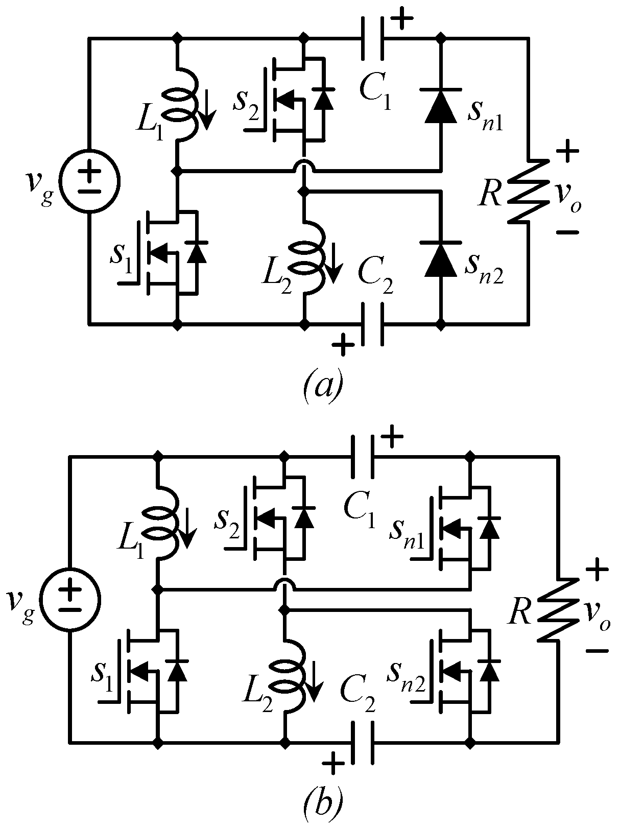
2. Proposed Converter Topology

Figure 2a shows the proposed topology. Their step-up unidirectional version contains two inductors (L1 and L2), two capacitors (C1 and C2), two transistors (s1 and s2), and two diodes (sn1 and sn2). As in other DC–DC converter topologies, the basic topology (Figure 2a) has a unidirectional power flow since diodes can drain current in one direction. However, with the addition of antiparallel transistors with diodes, what we call synchronous rectification provides bidirectional power flow (along with a possibly better efficiency). The bidirectional version of the converter is shown in Figure 2b.
The connection of the topology allows for operation with two capacitors whose voltage is smaller than the output voltage, as further explained in the paper. Furthermore, the voltage from the input reference to the output reference is floating, as in other state-of-the-art topologies (see Figure 1), but in this case, the voltage is non-pulsating, which reduces the noise and common mode current. Another advantage of the proposed topology is that their bidirectional power-flow configuration can be made with two half-bridges, which are commercial, off-the-shelf products.
By applying Kirchhoff’s voltage law in the external loop of the circuit in Figure 2 and considering the polarities defined for voltage in capacitors, the output voltage can be expressed as (1).
v o = v g + v C 1 + v C 2
An important note about the circuit (see Figure 2 and Equation (1)), as further explained later, is that no capacitor sustains the output voltage.
In this case, the output voltage is provided by the summation of the input voltage source and two series-connected capacitors. In other topologies available in the literature (see Figure 1), a capacitor is rated to the output voltage. This capacitor may store a significant amount of energy, which is related to the size of the capacitor.
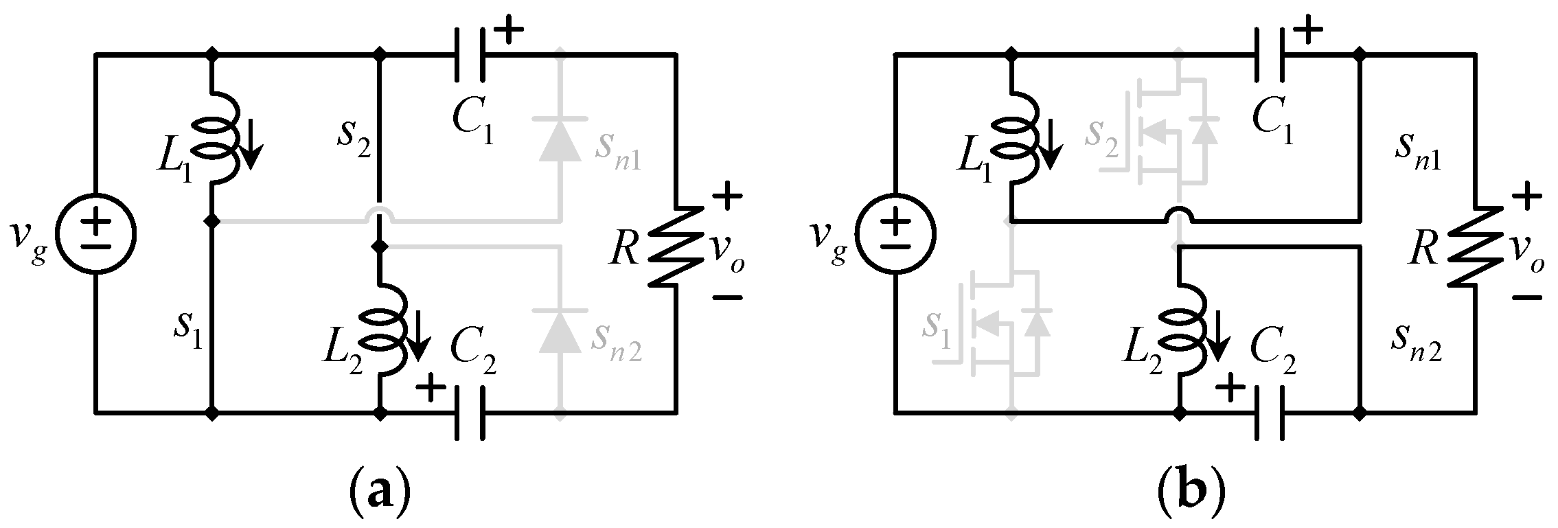
Transistors of the proposed converter have the same switching functions. In the continuous conduction mode (CCM), this operation leads to two possible equivalent circuits according to the switching state; see Figure 3. The current direction and voltage polarities follow the passive components’ sign convention.

2.1. Theoretical Waveforms

Figure 4 shows the theoretical waveforms for inductors from top to bottom, respectively: the inductors’ currents (iLx, x = 1, 2.), the inductors’ voltages (vLx, x = 1, 2.), and the firing signals (sx, x = 1, 2.); both inductors have similar waveforms. The firing signal is a digital signal that switches from high to low, thus closing and opening switches.
The inductor voltage is a DC signal whose average value is IL, and it has a triangular switching ripple that can be explained in the following manner: when switches are closed, the converter behaves as in Figure 3a. Inductors are connected to the input voltage Vg, and the current through inductors rises with a slope of (Vg/Lx). When switches are open, the converter behaves as in Figure 3b. Inductors are connected to their respective capacitors (Cx, x = 1, 2.), and the current through inductors decreases with a slope of (−VCx/Lx).
The voltage through inductors looks like a rectangular waveform. The steady state is reached when the area under the curve during the first semi-cycle (VgDTS) equals the area under the curve during the second semi-cycle ((1 − D)TS(VCx)).
It is considered that the input voltage is a DC signal, so the rising slope of the current is almost constant. Something similar happens to the falling slope. During this time, the capacitor is charging and the negative voltage across the inductor is decreasing (becoming more negative). As can be seen, we could choose to have a very small voltage ripple (for example, 1%) the capacitor, which would make the signal look rectangular.
Figure 5 shows the theoretical waveforms corresponding to capacitors from top to bottom, respectively: the voltages of the capacitors (vCx, x = 1, 2.), the capacitors’ currents (iCx, x = 1, 2.), and the firing signals (sx, x = 1, 2.); both capacitors have similar waveforms. The firing signal for transistors is the same as in Figure 4 and is included to give an idea of the synchronization.
When switches are closed, the converter behaves as in Figure 3a. Capacitors are discharged with the output current Io, and the voltage across capacitors decreases with a slope of (−Io/Cx). When switches are open, the converter behaves as in Figure 3b. Capacitors are charged with the inductor currents, and the voltage is increasing with a slope of ((IL − Io)/Cx). The current through capacitors looks like a rectangular waveform. The steady state is reached when the area under the curve during the first semi-cycle (IoDTS) equals the area under the curve during the second semi-cycle (1 − D)TS(ILx − Io).
Since the current ripple in inductors is usually larger than the voltage ripple in capacitors, the current charging the capacitor has a ripple that seems more significant and the rising slope of the capacitor voltage seems slightly curved.

2.2. Converter’s Mathematical Model

Let us now discuss the mathematical model of the converter. With the description of the circuit and the equivalent circuits shown in Figure 2, the standard averaging technique can be used to write the mathematical model of the converter [1,2,3].
The average voltage across inductors L1 and L2 during one switching cycle can be expressed as (2) and (3), respectively.
L 1 d i L 1 d t = d ( v g ) + ( 1 d ) ( v C 1 )
L 2 d i L 2 d t = d ( v g ) + ( 1 d ) ( v C 2 )
The first term of the right side of Equation (2), dvg, represents the voltage across L1 when the transistor is closed (vg) multiplied by the average time in which the transistor is closed (d). The second term of Equation (2), (1 − d)(−vC1), represents the voltage across L1 when the transistor is open (−vC1) times the average time in which the transistor is open (1 − d).
Similarly, the averaging technique can be applied to the current through capacitors. The average current through capacitors C1 and C2 can be expressed as (4) and (5), respectively.
C 1 d v C 1 d t = d ( v o R ) + ( 1 d ) ( i L 1 v o R )
C 2 d v C 2 d t = d ( v o R ) + ( 1 d ) ( i L 2 v o R )
where the first term d(−vo/R) represents the current through C1 when transistors are closed (−vo/R) multiplied by the average time transistors are closed d. The second term in equation (4) represents the current through capacitor C1 when transistors are open (iL1 − vo/R) multiplied by the average time in which transistors are closed (1 − d).
The set of Equations (2) to (5) is the average dynamic model of the converter. Before analyzing the model, Equations (2) to (5) can be simplified by algebraic manipulation and rewritten as Equations (6) to (9).
L 1 d i L 1 d t = d v g ( 1 d ) v C 1
L 2 d i L 2 d t = d v g ( 1 d ) v C 2
C 1 d v C 1 d t = ( 1 d ) i L 1 i o
C 2 d v C 2 d t = ( 1 d ) i L 2 i o
The output current io is present in the system and can be expressed in terms of the output voltage (1) and the output resistance R. This model considers CCM operation.
As can be seen from the dynamic model (6)–(9), the average model is non-linear. This also happens to other topologies, such as that of a traditional boost converter; there are several ways to deal with this, such as small AC signal linearization, in which signals are represented by the sum of their DC component plus an AC component, the DC component is usually the equilibrium or steady-state condition (which is introduced in Section 2.3), and the AC component is the component that contains deviations from the equilibrium, such as transient oscillations; this technique was used in [1].

2.3. DC Components of State Equations or Equilibrium Operation Point

From the dynamic Equations (6) to (9), the equilibrium operation point can be calculated considering the small ripple approximation [1], which can be summarized as variables in (6) to (9) appearing in the lower case, indicating that they are not constant values. The small ripple approximation considers that changes on the state variables are negligibly small (during a single switching cycle), which can be accomplished via the good selection of the switching frequency, capacitance in capacitors, and inductance in inductors. In the steady state, the derivative of state variables is zero. Then, after making (6) equal to zero and considering the small ripple approximation, the voltage in C1 can be expressed as (10).
V C 1 = D 1 D V g
DC values obtained with the small ripple approximation are indicated in capital letters. With the same procedure, from (7), the voltage across C2 can be expressed as:
V C 2 = D 1 D V g
Then, from (1), (10) and (11), the output voltage can be expressed in the steady state as (12).
V o = V g 1 + D 1 D
The current through inductors L2 and L1 can also be expressed from (9) and (10), respectively, as (13) and (14) from the same procedure that leads to (10) and (11).
I L 2 = 1 ( 1 D ) V o R
I L 1 = 1 ( 1 D ) V o R
We can make some remarks about the obtained result. The voltage gain expressed in (12) is the same as that for the previous converter (the one in Figure 1). Both converters offer a larger voltage gain compared with a traditional boost converter for the same duty cycle. However, an advantage is that capacitors sustain a lower voltage in the proposed converter. Figure 6 shows two graphs: (i) In blue, the voltage gains of the converter as a function of the duty cycle—which is basically (12) divided over the input voltage Vg for the former topology—is the same as the voltage in the output capacitor since the output capacitor sustains the output voltage; (ii) in red, the function of the voltage across capacitors of the proposed converter—basically (10) or (11) divided over the input voltage Vg—is shown to be substantially smaller than the blue graph.
For example, let us consider a converter that operates with an input voltage of 100 V and an output voltage of 300 V. The former topology would require a capacitor to sustain 300 V, while the proposed topology would require two capacitors of 100 V. We must also consider that the input-to-output reference has a continuous (non-pulsating) voltage.
The stored energy in a capacitor is a function of its voltage and capacitance, according to (15).
E C = C V C 2 2
We can observe the stored energy in a capacitor is proportional to the square of its voltage, for which a reduction in the voltage of a capacitor would result in a reduction in stored energy. Furthermore, the volume of a capacitor is linearly dependent on its stored energy [14,15,16].

2.4. Selection of Inductors and Capacitors

This section discusses the selection of reactive components based on the maximum ripple allowed for the state variables.
Inductors L1and L2: Both inductors have the classical waveform of inductor current in switched-mode power supplies; this is a DC component plus an AC triangular variation. The DC component depends on the voltage gain (or duty cycle) and the load; see (13) and (14). The variation is usually called ripple, and it depends on more parameters, such as the switching frequency FS (or their inverse, the switching period TS), the duty cycle, and the inductance. The inductance is then selected according to the desired ripple as follows.
From Figure 3, it can be seen that when transistor s1 is on, its terminal voltage is equal to Vg, and then its current rises with a slope equal to Vg/L1. This situation holds for a time equal to DTS. In the field of power electronics, the current ripple used to be defined as half of the total current change (half the peak-to-peak ripple). In other words, we consider the ripple as the deviation from the average value of a signal. For the current through an inductor, this can be expressed as (16), and the inductance can be calculated as (17).
2 Δ i L 1 = V g L 1 D T S
L 1 = V g 2 Δ i L 1 D T S
Note that the small ripple approximation is considered in (17), and in all reactive elements sizing equations, (17) allows for the selection of L1 for a desired current ripple in L1. Since both switching stages have the same duty cycle, (17) can be used to calculate L2; in other words, we can make L1 = L2.
Capacitors C1 and C2: Capacitors can be calculated with a similar procedure to that of inductors, but the state variable is instead the voltage; the voltage in capacitors is a DC component plus an AC variation, and the DC component depends on the voltage gain (or duty cycle) and the input voltage. The AC variation depends on other parameters, including the current, switching frequency, and capacitance. The capacitance is then selected according to the desired ripple as follows.
When transistor s1 is open, the current through capacitor C1 is equal to the output current. A negative sign may be considered to indicate that the voltage is falling since the capacitor is being discharged, and then its voltage is being reduced with a slope equal to −Iout/C1. This situation holds during the time (1 − D)Ts, and during this period, the voltage drop can be expressed as Equation (18).
2 Δ v C 1 = I o u t C 1 ( 1 D ) T s
Negative signs indicate a voltage drop. From (18), the capacitor C1 can be selected to comply with the desired voltage ripple ΔvC1 in C1 by following (19).
C 1 = I o u t 2 Δ v C 1 ( 1 D ) T S
Equation (19) allows for the selection of C1 for the desired voltage ripple in C1. Since both switching stages have the same duty cycle, (19) can be used to calculate C2. In other words, we can make C1 = C2.

2.5. Selection of Semiconductors

The main data needed to choose semiconductors are the voltage they need to block when they are open and the current they drain when they are closed. It can be observed from Figure 3b that both transistors (as well as both diodes) are rated to the same voltage, which is the input voltage plus the voltage in a capacitor; this can be expressed as (20).
V s w i t c h = V g + V C = V g + D 1 D V g = 1 1 D V g
The voltage rating of the switch is expressed with the same function as the voltage rating in a boost converter. Still, due to the different voltage gain functions, the proposed converter requires transistors rated to a smaller voltage, as is shown in Section 5.
Figure 3a shows that the current through transistors when they are closed is equal to the current through inductors. Then, the average current through transistors can be expressed as (21).
I S w i t c h = D I L = D ( 1 D ) I o
Again, the current through switches seems equal to that in a traditional boost, but the proposed converter would require a smaller duty cycle to achieve an equivalent voltage gain for which the current rating of transistors is again smaller; see Section 5.
If switches are synthesized with IGBTs, the average current is enough to calculate their conduction losses, but if MOSFETs are used instead, the RMS current is required. The RMS current through transistors can be expressed as:
I R M S S w i t c h = I L D 1 + 1 3 ( Δ i L I L ) 2
Consider here that ΔiL is as defined in (16) and IL is as defined in (13) and (14).
The average current of diodes can also be determined by considering Figure 3a and using the averaging technique. When closed, the current through diodes is equal to the current through inductors, and the average current through diodes can be expressed as (23).
I S w i t c h = ( 1 D ) I L = I o
If synchronous rectification is required, the RMS current needs to be calculated to evaluate conduction losses. The RMS current can be expressed as:
I R M S D i o d e = I L ( 1 D ) 1 + 1 3 ( Δ i L I L ) 2
Consider here that ΔiL is as defined in (16) and IL is as defined in (13) and (14).

3. Gain Considering Losses and Efficiency Calculations

This section analyzes two important aspects of the converter related to power losses. First is the gain considering losses; the real gain may differ from Equation (12) and Figure 6 due to some power losses. Second, the loss calculation in each element of the converter is shown.

3.1. Real Voltage Gain Considering Losses

Figure 7 shows a circuit equivalent to the proposed topology in which ideal elements are drawn with their Equivalent Series Resistance (ESR) to indicate their conduction losses. In this section, the considered elements are inductors and switches since they have dominant effects on the real voltage gain. In the efficiency section, capacitor losses are also calculated. RL1 and RL2 are the ESR of inductors L1 and L2, respectively. RS1, RS2, RS1n, and RS2n are the on-resistance of switches. This model considers the converter to have synchronous rectification; see Figure 2b.
Figure 8 shows the equivalent circuits of the converter according to the switching state; Figure 8a shows the state in which transistors s1 and s2 are closed while s1n and s2n are open, and Figure 8b shows the state in which transistors s1n and s2n are closed while s1 and s2 are open.
According to those equivalent circuits (see Figure 8), the dynamic equations for inductors (in other words, the average voltage across inductors L1 and L2 during one switching cycle) can be expressed as (25) and (26), respectively.
L 1 d i L 1 d t = d ( v g i L 1 R L 1 i L 1 R S 1 ) + ( 1 d ) ( v C 1 i L 1 R L 1 i L 1 R S 1 n )
L 2 d i L 2 d t = d ( v g i L 2 R L 2 i L 2 R S 2 ) + ( 1 d ) ( v C 2 i L 2 R L 2 i L 2 R S 2 n )
Equations (25) and (26) contain the voltage drops in ESR of elements in series with inductors when they are charging and discharging. Similarly, the averaging technique can be applied to the current through capacitors. The average current through capacitors C1 and C2 can be expressed as (27) and (28), respectively.
C 1 d v C 1 d t = d ( v o R ) + ( 1 d ) ( i L 1 v o R )
C 2 d v C 2 d t = d ( v o R ) + ( 1 d ) ( i L 2 v o R )
Note that in this case, (27) and (28) are equal to (4) and (5) since there is not a current drop effect. The set of Equations (22) to (28) is the average dynamic model of the converter considering conduction losses. If we consider that all transistors are of the same type, their ESR must be similar. We can call RS the ESR of all transistors; this allows us to simplify Equations (25) to (28) and rewrite them as Equations (29) to (32).
L 1 d i L 1 d t = d v g ( 1 d ) v C 1 ( R L 1 + R S ) i L 1
L 2 d i L 2 d t = d v g ( 1 d ) v C 2 ( R L 2 + R S ) i L 2
C 1 d v C 1 d t = ( 1 d ) i L 1 i o
C 2 d v C 2 d t = ( 1 d ) i L 2 i o
In this case, the equilibrium equations cannot be directly obtained, as we did it with (10) and (11) since the current is present in (29) and (30). However, as explained in [1], the current relationships are in the steady state in (31) and (32) and are then substituted to obtain the voltages in equilibrium. Considering the equilibrium operation from (29) and (30), the following expressions can be written.
D V g = ( 1 D ) V C 1 + ( R L 1 + R S ) I L 1
D V g = ( 1 D ) V C 2 + ( R L 2 + R S ) I L 2
From (31) and (32), the current relationship in the equilibrium can be expressed as (35) and (36).
I L 1 = 1 ( 1 D ) I o
I L 2 = 1 ( 1 D ) I o
Due to the symmetry of the circuit and Equations (33)–(36), the current through inductors are equal; see (35) and (36). Then, both capacitors have the same voltage; see (33) and (34). We can simplify these to (37).
V C = V C 1 = V C 2
By applying the KVL in Figure 7 and considering (37), the output voltage can be expressed as (38).
V o = V g + V C 1 + V C 2 = V g + 2 V C
The output current can also be expressed as (39).
I o = V g + V C 1 + V C 2 R = V g + 2 V C R
By substituting (37) with (33), we can obtain:
D V g = ( 1 D ) V C 1 + ( R L 1 + R S ) 1 ( 1 D ) I o
D V g = ( 1 D ) V C 1 + ( R L 1 + R S 1 D ) ( V g + 2 V C 1 R )
D V g = ( 1 D ) V C 1 + ( R L 1 + R S ) V g ( 1 D ) R + ( R L 1 + R S ) 2 V C 1 ( 1 D ) R
D V g ( R L 1 + R S ) V g ( 1 D ) R = ( 1 D ) V C 1 + ( R L 1 + R S ) 2 V C 1 ( 1 D ) R
V g ( D ( R L 1 + R S ) ( 1 D ) R ) = ( ( 1 D ) + ( R L 1 + R S ) 2 ( 1 D ) R ) V C 1
V C 1 = V C 2 = V C = V g ( D ( R L 1 + R S ) ( 1 D ) R ) ( ( 1 D ) + ( R L 1 + R S ) 2 ( 1 D ) R )
Equation (45) provides us with the voltage in each capacitor considering the losses. The real gain depends on the percentage of RL1 and RS concerning the output resistance R. Note that if that parasitic resistance is equal to zero, (45) becomes (10) and (11).
Let us consider that parasitic resistors RL1 and RS are lumped in a single parasitic resistance RP.
R P = R L + R S
Figure 9 shows the gain of the converter considering conduction losses as a relation of RP/RL, as in Figure 3.9 in [1] for a traditional boost converter.
The relations among RP/RL in Figure 9 are relatively high for practical application, but we used the same relations as shown in Figure 3.9 in [1] for reference or a point of comparison. A traditional boost converter achieves a maximum gain of five when RP/RL = 0.01, while the proposed converter achieves a maximum gain of nine for the same relation.
A traditional boost converter achieves a maximum gain of around 3.5 when RP/RL = 0.02, while the proposed converter achieves a maximum gain of six for the same relation.

3.2. Efficiency Analysis

After calculating the new steady state (considering conduction losses), the voltage across capacitors VC1 and VC2 can be expressed with (45), and the current through inductors IL1 and IL2 as determined in (35) and (36), the current ripple in inductors ΔiL1 and ΔiL2 as expressed in (16), and the voltage ripple in capacitors ΔvC1 and ΔvC2 as expressed in (18) can be used to express the losses in each element.
The losses in inductors can be expressed as the RMS current square times their ESR, and the RMS current through inductors L1 and L2 can be expressed as (47) and (48).
I R M S L 1 = I L 1 1 + 1 3 ( Δ i L 1 I L 1 ) 2
I R M S L 2 = I L 2 1 + 1 3 ( Δ i L 2 I L 2 ) 2
The losses in capacitors are usually very small, but they can also be calculated as their RMS current times their ESR. As shown in Figure 5, the current through capacitors has a trapezoidal and rectangular segment. To express the RMS current through the trapezoidal segment, it is convenient to define the maximum current (of the trapezoid) termed IAux1 and the minimum current (of the trapezoid) termed IAux2, as defined in (49) and (50), respectively.
I A u x 1 = I L 1 I o + Δ i L 1
I A u x 2 = I L 1 I o Δ i L 1
The RMS current through capacitor C1 can be expressed as (51).
I R M S C 1 = D 1 3 ( I A u x 1 2 + I A u x 1 I A u x 2 + I A u x 2 2 ) + ( 1 D ) I o
Similarly, to express the RMS current through C2, it is convenient to define the maximum current (of the trapezoid) termed IAux3 and the minimum current termed IAux4, as defined in (52) and (53), respectively.
I A u x 3 = I L 2 I o + Δ i L 2
I A u x 4 = I L 2 I o Δ i L 2
The RMS current through the capacitor can be expressed as (54).
I R M S C 2 = D 1 3 ( I A u x 3 2 + I A u x 3 I A u x 4 + I A u x 4 2 ) + ( 1 D ) I o
The conduction losses of switches can also be calculated with their RMS current (square) times their on-resistance. When switches are closed, they drain the current through inductors, and their RMS current can be calculated as (55)–(58).
I R M S S 1 = I L 1 D 1 + 1 3 ( Δ i L 1 I L 1 ) 2
I R M S S 2 = I L 2 D 1 + 1 3 ( Δ i L 2 I L 2 ) 2
I R M S S 1 n = I L 1 1 D 1 + 1 3 ( Δ i L 1 I L 1 ) 2
I R M S S 2 = I L 2 1 D 1 + 1 3 ( Δ i L 2 I L 2 ) 2
Switches s1 and s2 also have switching losses in both the turn-on and the turn-off transitions; their switching losses can be estimated with the triangular approximation.
s 1 s w L o s s = 0.5 Δ t o f f ( I L 1 + Δ i L 1 ) ( V C 1 Δ v C 1 ) f S + 0.5 Δ t o n ( I L 1 Δ i L 1 ) ( V C 1 + Δ v C 1 ) f S
s 2 s w L o s s = 0.5 Δ t o f f ( I L 2 + Δ i L 2 ) ( V C 2 Δ v C 2 ) f S + 0.5 Δ t o n ( I L 2 Δ i L 2 ) ( V C 2 + Δ v C 2 ) f S
where fS is the transistor switching frequency. Those calculations are useful to determine the power losses in each element, as well as the efficiency of the converter.
The loss calculations were performed and are included in Section 6, along with the efficiency measured from the experimental prototype. The losses used for the calculated efficiency are shown in Table 1.

4. Comparative Evaluation

This section compares a particular design with two converters: (i) the converter proposed in [9] and shown in Figure 1 and (ii) the proposed converter. This is useful for understanding the advantages of the proposed converter. For the comparison, a particular design with some specifications is solved with both converters, and the result is compared; the advantage of the proposed topology is that it requires less stored energy in the capacitors. The presented comparison can be validated with a computer simulation via commercial software such as Synopsys Saber, PLECS, and PSIM.
Converters have different numbers of capacitors, but we can establish equivalencies based on the stored energy. The proposed converter’s main advantage is the capacitor’s voltage rating, which reduces the stored energy. The energy stored in capacitors strongly depends on their size [14,15,16].

4.1. Specifications

The objective of this study was to design a converter fed with 20 V, which required stepping it up to 100 V. The switching frequency was set to 50 kHz. The peak-to-peak output voltage ripple specification was set to 3 V (1.5 volts peak), representing 3% of the output voltage. The specification was given as maximum values. Evidently, one may choose smaller capacitors, but they may not comply with the spec. The spec was tested at 100 W of output power (Io = 1 A).

4.2. Solution to the Design

Figure 10 shows the solution to the design with the converter in [9]; this converter required a 4.44 µF capacitor to comply with the specified peak-to-peak ripple of 3 V; we chose a commercial value of 5 µF, which resulted in a peak-to-peak ripple of 2.6 V (1.3 V peak) and the storage of 25.7 mJ of energy. Figure 11 shows the solution to the design with the proposed converter. This converter required an 8.88 µF capacitor to comply with the specified peak-to-peak ripple of 3 V. We chose a commercial value of 10 µF, resulting in a peak-to-peak ripple of 2.6 V (1.3 V peak). This matched both designs to the same output voltage ripple. The design with the proposed converter could store 16.9 mJ of energy. The stored energy in the capacitors led to a significant reduction. The proposed converter required only 65% of the stored energy in capacitors compared with the first solution.

5. Simulation Results

To corroborate the operation of the proposed converter, the converter was simulated in the software Synopsys Saber in a computer with an Intel i7 processor (11th Gen i7-1165G7 at 2.80 GHz), 32 GB of RAM, and Windows 11 Pro (64 bits). Figure 12 shows the simulation schematics of the bidirectional (or synchronous rectified) version.
Table 2 shows the parameters of the simulation. According to equilibrium Equations (10)–(14), the output voltage was expected to be 100 V and the voltage across capacitors was equal to 40 V. In most step-up converters, there is an output capacitor rated to the output voltage (100 V in this case) since the volume of capacitors is proportional to their stored energy, and the stored energy is proportional to the square of their voltage rating. A reduction in the voltage rating is an advantage.
Figure 13 shows a comparison of the output voltage, around 100 V in this case, and the voltage across capacitors, around 40 V in this case.
Figure 14 shows a zoom into the output voltage. Two waveforms are shown in Figure 14 because, in this case, we included the version without synchronous rectification (only diodes for s1n and s2n) (see Figure 2a) and the version with synchronous rectification (see Figure 2b). The real voltage was slightly smaller than 200 V due to the losses in devices (the simulation was performed considering non-ideal elements). Still, the synchronous rectification had a slightly lower voltage since the on-voltage on diodes was larger than the voltage drops in MOSFETS.

6. Experimental Results

A small prototype was built to demonstrate the principle of the proposed topology. The prototype was based on the Transphorm brand TDHB-65H070L-DC half-bridge (the Digi-Key part number is TDHB-65H070L-DC-ND), which is made of TP65H070L series GaN FETs. Figure 15 shows a diagram of the prototype, as well as the used capacitor and inductor types. The capacitors were the 10 µF EXH2E106HRPT from the Nichicon brand (their Digi-Key part number is 493-13827-ND), and the inductors were the 250 µH ATCA-08-251M-V from the Abracon LLC brand (their Digi-Key part number is 535-13513-ND).
To connect the GaN FETs boards, a Transphorm brand TDHBG1200DC100-KIT motherboard was used. Figure 16 shows a photo of the prototype connected to the test bench.
Figure 17 shows the waveforms related to L1, as in Figure 4, for a particular operating point in which the duty cycle D = 0.66, the input voltage was around 20 V, the output voltage was around 100 V, and the output power was around 100 W.
Figure 18 was captured at the same operating conditions, but it shows the current through the two inductors (they had the same amplitude and shape). Figure 18 also shows the output voltage.
The top signal in Figure 17 is the current through an inductor (L1), and it looks like a DC plus a triangular waveform; it is shown at 2 A/div, and the triangular increased to slightly more than 1 A during the time in which its transistor (s1) was closed. The time lasted for D/fS (D = 0.66 and fS = 50 kHz), which was the time in which transistors were closed, and it turned out to be around 13.2 µS. The oscillogram was captured at 10 µS/Div.
The voltage across the inductor is shown below the inductor current in Figure 17; when the switch was closed (which coincided with the positive slope in the inductor), the voltage across the inductor was the input voltage (20 V); the inductor voltage was captured with a Tektronix P5200A voltage prove at 50 V/div. When the transistor was open, the voltage across the inductor was negative (which coincided with the negative slope in the inductor current). The inductor had the same voltage across the capacitor (but negative), which was around −40 V under these operating conditions.
Finally, the voltage across the switch s1 at the bottom of Figure 17 in pink; it was almost zero when the switch was closed and Vg + VC1 when the switch was open; in these operating conditions, its value turned out to be around 60 V.
Figure 19 shows the efficiency measured for different operating conditions. The line in Figure 19 shows the calculated efficiency according to the procedure in Section 3. Points are measurements of the efficiency in particular operating conditions.

7. Conclusions

This paper introduces a transformer-less DC–DC converter topology that provides a high voltage gain without an extreme duty cycle. The main advantage of the proposed topology compared with other similar circuits is that capacitors are rated to a reduced voltage. Furthermore, the voltage among the ground input and output is not pulsating, and their synchronous rectified version can be synthesized with commercial, off-the-shelf transistors in half-bridge packages. Reducing the voltage rating in capacitors is advantageous since the physical size of capacitors depends on the stored electrical energy, which depends on the square of their voltage. The steady-state analysis of the proposed converter in the continuous conduction mode is presented along with their large-signal and linearized small-signal models. Future work will be dedicated to the study of their dynamics and control. The paper also presents a design procedure that includes the selection of capacitors and inductors and their maximum voltage and current values for an application example. For this particular design with specifications, the proposed converter required only 65% of the stored energy in capacitors compared with a similar converter in the literature. Finally, the results from a computer-based simulation and from an experimental test bench verified the principle of the operation of the proposed converter. The experimental prototype was able to achieve a peak efficiency of over 96%.

Author Contributions

J.C.R.-C. and J.E.V.-R. contributed to the conceptualization of the article from the power electronics point of view; S.O.-C. and J.R. contributed the methodology; J.C.M.-M. and M.R.-C. contributed the software, validation, and formal analysis; and A.V.-G. and J.C.R.-C. wrote the draft and manuscript preparation. All authors have read and agreed to the published version of the manuscript.

Funding

The authors would like to thank Universidad Panamericana for their support through the program “Fomento a la Investigación UP 2022” and project “Estudio de topologías de convertidores de cd-cd” UP-CI-2022-GDL-06-ING.

Data Availability Statement

Not applicable.

Acknowledgments

The authors would like to thank: Universidad Panamericana, Centro de Investigación y de Estudios Avanzados del Instituto Politécnico Nacional CINVESTAV del IPN, Tecnologico de Monterrey, and to The University of Sheffield.

Conflicts of Interest

The authors declare no conflict of interest.

References

  1. Erickson, R.W.; Maksimovic, D. Fundamentals of Power Electronics; Springer: New York, NY, USA, 2001. [Google Scholar]
  2. Rashid, M. Power Electronics: Circuits, Devices and Applications, 3rd ed.; Prentice Hall: London, UK, 2004; p. 762. [Google Scholar]
  3. Undeland, M.N.; Robbins, W.P.; Mohan, N. Power Electronics. In Converters, Applications, and Design, 3rd ed.; John Whiley & Sons: Hoboken, NJ, USA, 1995; p. 763. [Google Scholar]
  4. Reyes-Portillo, I.A.; Claudio-Sanchéz, A.; Morales-Saldaña, J.A.; Mina-Antonio, J.D.; Netzahuatl-Huerta, E.M.; Claudio-Pachecano, L.; Ponce-Silva, M.; Reyes-Sánchez, E. Study of the Effects of Current Imbalance in a Multiphase Buck Converter for Electric Vehicles. World Electr. Veh. J. 2022, 13, 88. [Google Scholar] [CrossRef]
  5. Loera-Palomo, R.; Morales-Saldaña, J.A.; Rivero, M.; Álvarez-Macías, C.; Hernández-Jacobo, C.A. Noncascading Quadratic Buck-Boost Converter for Photovoltaic Applications. Micromachines 2021, 12, 984. [Google Scholar] [CrossRef] [PubMed]
  6. López-Santos, O.; Varón, N.L.; Rosas-Caro, J.C.; Mayo-Maldonado, J.C.; Valdez-Reséndiz, J.E. Detailed Modeling of the Low Energy Storage Quadratic Boost Converter. In IEEE Transactions on Power Electronics; IEEE: Piscataway, NJ, USA, 2022; Volume 37, pp. 1885–1904. [Google Scholar]
  7. Rosas-Caro, J.C.; Ramirez, J.M.; Peng, F.Z.; Valderrabano, A. A DC–DC multilevel boost converter. IET Power Electron. 2010, 3, 129–137. [Google Scholar] [CrossRef]
  8. Lenk, R. Practical Design of Power Supplies; IEEE-Press: Piscataway, NJ, USA; Wiley-Interscience Publishers: Hoboken, NJ, USA, 2005. [Google Scholar]
  9. Yang, L.S.; Liang, T.J.; Chen, J.F. Transformerless DC–DC Converters with High Step-Up Voltage Gain. IEEE Trans. Ind. Electron. 2009, 56, 3144–3152. [Google Scholar] [CrossRef]
  10. Yang, L.; Liang, T. Analysis and Implementation of a Novel Bidirectional DC-DC Converter. IEEE Trans. Ind. Electron. 2012, 59, 422–434. [Google Scholar] [CrossRef]
  11. Lin, X.; Wang, F.; Iu, H.H.C. A New Bridgeless High Step-up Voltage Gain PFC Converter with Reduced Conduction Losses and Low Voltage Stress. Energies 2018, 11, 2640. [Google Scholar] [CrossRef] [Green Version]
  12. Liao, H.; Chen, Y.-T.; Chen, L.; Chen, J.-F. Development of a Bidirectional DC–DC Converter with Rapid Energy Bidirectional Transition Technology. Energies 2022, 15, 4583. [Google Scholar] [CrossRef]
  13. Zhang, H.; Chen, Y.; Park, S.-J.; Kim, D.-H. A Family of Bidirectional DC–DC Converters for Battery Storage System with High Voltage Gain. Energies 2019, 12, 1289. [Google Scholar] [CrossRef] [Green Version]
  14. Husev, O.; Shults, T.; Vinnikov, D.; Roncero-Clemente, C.; Romero-Cadaval, E.; Chub, A. Comprehensive Comparative Analysis of Impedance-Source Networks for DC and AC Application. Electronics 2019, 8, 405. [Google Scholar] [CrossRef]
  15. Ponniran, A.B.; Orikawa, K.; Itoh, J. Minimum Flying Capacitor for N-Level Capacitor DC/DC Boost Converter. In IEEE Transactions on Industry Applications; IEEE: Piscataway, NJ, USA, 2016; Volume 52, pp. 3255–3266. [Google Scholar]
  16. Lefevre, G.; Mollov, S.V. A Soft-Switched Asymmetric Flying-Capacitor Boost Converter With Synchronous Rectification. In IEEE Transactions on Power Electronics; IEEE: Piscataway, NJ, USA, 2016; Volume 31, pp. 2200–2212. [Google Scholar]
Figure 1. One of the boost-type topologies in [9].
Energies 15 07944 g001
Figure 2. Proposed circuit: (a) unidirectional power flow and (b) bidirectional power flow.
Energies 15 07944 g002
Figure 3. Equivalent circuits, according to the switching state, (a) when transistors are closed and (b) when transistors are open.
Energies 15 07944 g003
Figure 4. Important waveforms related to the inductor from top to bottom, respectively: inductor current, inductor voltage, and switching function.
Energies 15 07944 g004
Figure 5. Important waveforms related to the capacitors from top to bottom, respectively: capacitor voltage, current, and switching function.
Energies 15 07944 g005
Figure 6. Voltage gains as a function of the duty cycle for the proposed and traditional boost converters.
Energies 15 07944 g006
Figure 7. Proposed circuit with series losses through inductors and transistors.
Energies 15 07944 g007
Figure 8. Equivalent circuits according to the switching state. Proposed circuit with series losses through inductors and transistors (a) when transistors are closed (b) when transistors are open.
Energies 15 07944 g008
Figure 9. Voltage gains as a function of the duty cycle considering conduction losses in the parasitic resistance of elements.
Energies 15 07944 g009
Figure 10. Solution with the topology in [9].
Energies 15 07944 g010
Figure 11. Solution with the proposed topology.
Energies 15 07944 g011
Figure 12. Schematic of the simulated converter.
Energies 15 07944 g012
Figure 13. Output voltage and the voltage across capacitors.
Energies 15 07944 g013
Figure 14. Zoom in the output voltage.
Energies 15 07944 g014
Figure 15. Experimental prototype diagram and main part photos.
Energies 15 07944 g015
Figure 16. Experimental prototype photo.
Energies 15 07944 g016
Figure 17. Current and voltage in L1, as well as the voltage across switch s1.
Energies 15 07944 g017
Figure 18. Current through inductors, output voltage, and the voltage across s1.
Energies 15 07944 g018
Figure 19. Calculated efficiency (line) and measured (points).
Energies 15 07944 g019
Table 1. Parameters.
The Inductance of Inductors L1 and L1L1 = L2 = 250 µH
Inductors’ ESR50 mΩ
Capacitor C1 and C2C1 = C2 = 10 µF
Capacitors’ ESR5 mΩ
Switching Frequency FSFS = 50 kHz
Transistors’ On-Resistance85 mΩ
Transistors’ On an Off time100 nS
Input Voltage VgVg = 20 V
Duty Cycle D0.66
Output Power0 to 300 W
Table 2. Parameters.
Inductor L1 and L1L1 = 250 µH, L2 = 250 µH
Capacitor C1 and C2C1 = 10 µF, C2 = 10 µF
Switching Frequency FSFS = 50 kHz
Input Voltage VgVg = 20 V
Output Load Resistance RR = 100 Ω
Publisher’s Note: MDPI stays neutral with regard to jurisdictional claims in published maps and institutional affiliations.

