Article

A Theoretical Investigation on the Physical Properties of Zirconium Trichalcogenides, ZrS3, ZrSe3 and ZrTe3 Monolayers

by
Bohayra Mortazavi
1,*,
Fazel Shojaei
2,
Mehmet Yagmurcukardes
3,
Meysam Makaremi
4 and
Xiaoying Zhuang
1,5,*
1
Chair of Computational Science and Simulation Technology, Department of Mathematics and Physics, Leibniz Universität Hannover, Appelstraße 11, 30167 Hannover, Germany
2
Department of Chemistry, Faculty of Nano and Bioscience and Technology, Persian Gulf University, Bushehr 75169, Iran
3
Department of Photonics, Izmir Institute of Technology, 35430 Izmir, Turkey
4
Independent Researcher, Whitehall, MI 49461, USA
5
College of Civil Engineering, Department of Geotechnical Engineering, Tongji University, 1239 Siping Road, Shanghai 200070, China
*
Authors to whom correspondence should be addressed.
Energies 2022, 15(15), 5479; https://doi.org/10.3390/en15155479
Submission received: 17 June 2022 / Revised: 5 July 2022 / Accepted: 27 July 2022 / Published: 28 July 2022
(This article belongs to the Special Issue Advances in Energy Materials and Clean Energy Technologies)

Abstract

:
In a recent advance, zirconium triselenide (ZrSe3) nanosheets with anisotropic and strain-tunable excitonic response were experimentally fabricated. Motivated by the aforementioned progress, we conduct first-principle calculations to explore the structural, dynamic, Raman response, electronic, single-layer exfoliation energies, and mechanical features of the ZrX3 (X = S, Se, Te) monolayers. Acquired phonon dispersion relations reveal the dynamical stability of the ZrX3 (X = S, Se, Te) monolayers. In order to isolate single-layer crystals from bulk counterparts, exfoliation energies of 0.32, 0.37, and 0.4 J/m2 are predicted for the isolation of ZrS3, ZrSe3, and ZrTe3 monolayers, which are comparable to those of graphene. ZrS3 and ZrSe3 monolayers are found to be indirect gap semiconductors, with HSE06 band gaps of 1.93 and 1.01 eV, whereas the ZrTe3 monolayer yields a metallic character. It is shown that the ZrX3 nanosheets are relatively strong, but with highly anisotropic mechanical responses. This work provides a useful vision concerning the critical physical properties of ZrX3 (X = S, Se, Te) nanosheets.

Graphical Abstract

1. Introduction

After the experimental isolation of graphene [1,2,3] reported in 2004, two-dimensional (2D) nanomaterials have been extending continuously, owing to their exceptional physical and chemical properties. High surface-to-volume ratios in 2D systems can not only evolve to exceptional electronic and optical features, but are also highly appealing for practical chemistry-related applications, such as sensing and energy storage. In recent years, several 2D crystals with interesting physical properties have been fabricated, such as MoSi2N4 [4,5], fluorinated diamane [6], penta-palladium phosphide selenide (PdPSe) [7], niobium oxide diiodide (NbOI2) [8], penta-palladium phosphide sulfide (PdPS) [9], graphene-like BC2N [10], and penta-nickel diazenide (NiN2) [11] nanosheets. Highly bright prospects for the application of 2D nanomaterials in critical technologies and their outstanding physical and chemical features act as a continuous driving force for experimental endeavors to design and fabricate novel crystals. In line with continuous experimental accomplishments in the field of 2D nanomaterials, most recently Li et al. [12] succeeded in the exfoliation of the zirconium triselenide (ZrSe3) nanosheets. Experimental observations and theoretical calculations confirm highly anisotropic and strain-tunable semiconducting excitonic effects in ZrSe3 nanosheets [12]. This experimental advance also highlights the appealing possibility of the exfoliation of zirconium trisulfide and tritelluride (ZrS3 and ZrTe3) nanosheets, also with anisotropic and strain-tunable electronic and optical properties. As a novel class of synthesizable 2D materials, which have been already predicted to yield appealing thermoelectricity [13,14], the objective of this study is to theoretically explore the structural, phonon dispersion relations, Raman spectra, single-layer exfoliation energies, and mechanical features of ZrX3 (X = S, Se, Te) nanosheets by employing density functional theory (DFT) calculations.

2. Computational Methods

DFT calculations were carried out using the Vienna Ab-initio Simulation Package [15,16] with the GGA/PBE and DFT-D3 [17] vdW dispersion correction. The plane wave and self-consistent loop cutoff energies were set to 400 and 10−6 eV, respectively. In order to find optimized geometries, atomic positions were relaxed using a conjugate gradient algorithm until Hellman–Feynman forces dropped below 0.001 eV/Å [18] with an 11 × 11 × 1 and 9 × 9 × 5 Monkhorst–Pack [19] K-point grid for the monolayer and bulk systems, respectively. The stress-free structures were acquired by isotropically changing the in-plane lattice dimensions. Periodic boundary conditions were considered in all directions, with a 23 Å box-size along the out-of-plane direction of the monolayers to avoid artificial interactions. Moment tensor potentials (MTPs) [20] were fitted to evaluate the phonon dispersion relations, using the same approach as that employed in our recent work [21]. Phonon dispersions on the basis of trained MTPs were acquired in conjunction with the PHONOPY [22] code over 4 × 5 × 1 supercells, as elaborately discussed in our previous work [23]. For the investigation of Raman activities of each phonon mode, firstly, the zone-center phonon vibrations were calculated in terms of the phonon frequencies and the vibrational displacements. For each optical phonon mode, the derivative of the macroscopic dielectric tensor with respect to the normal mode of each vibration was investigated using the finite-difference method.

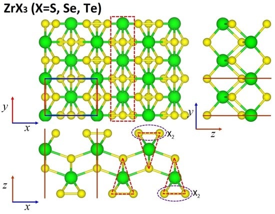
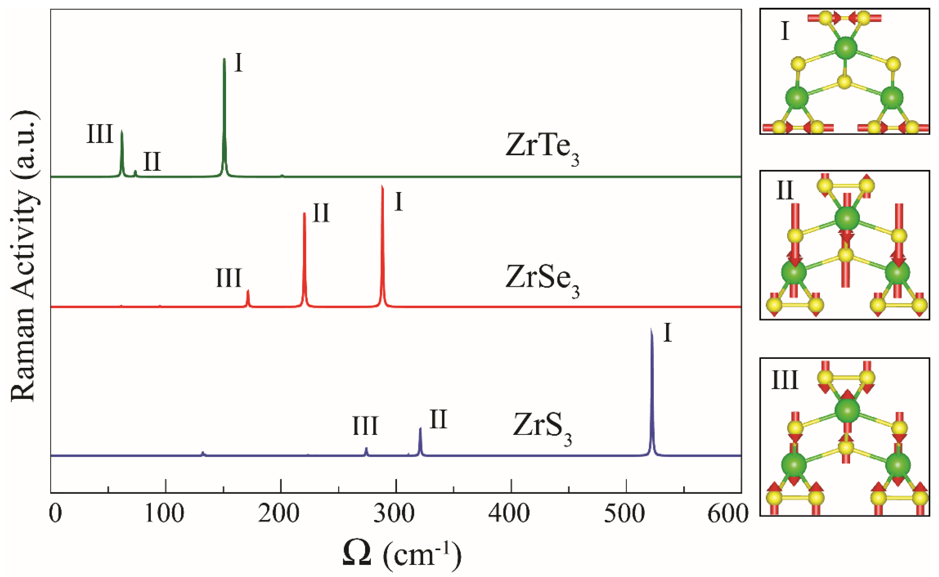
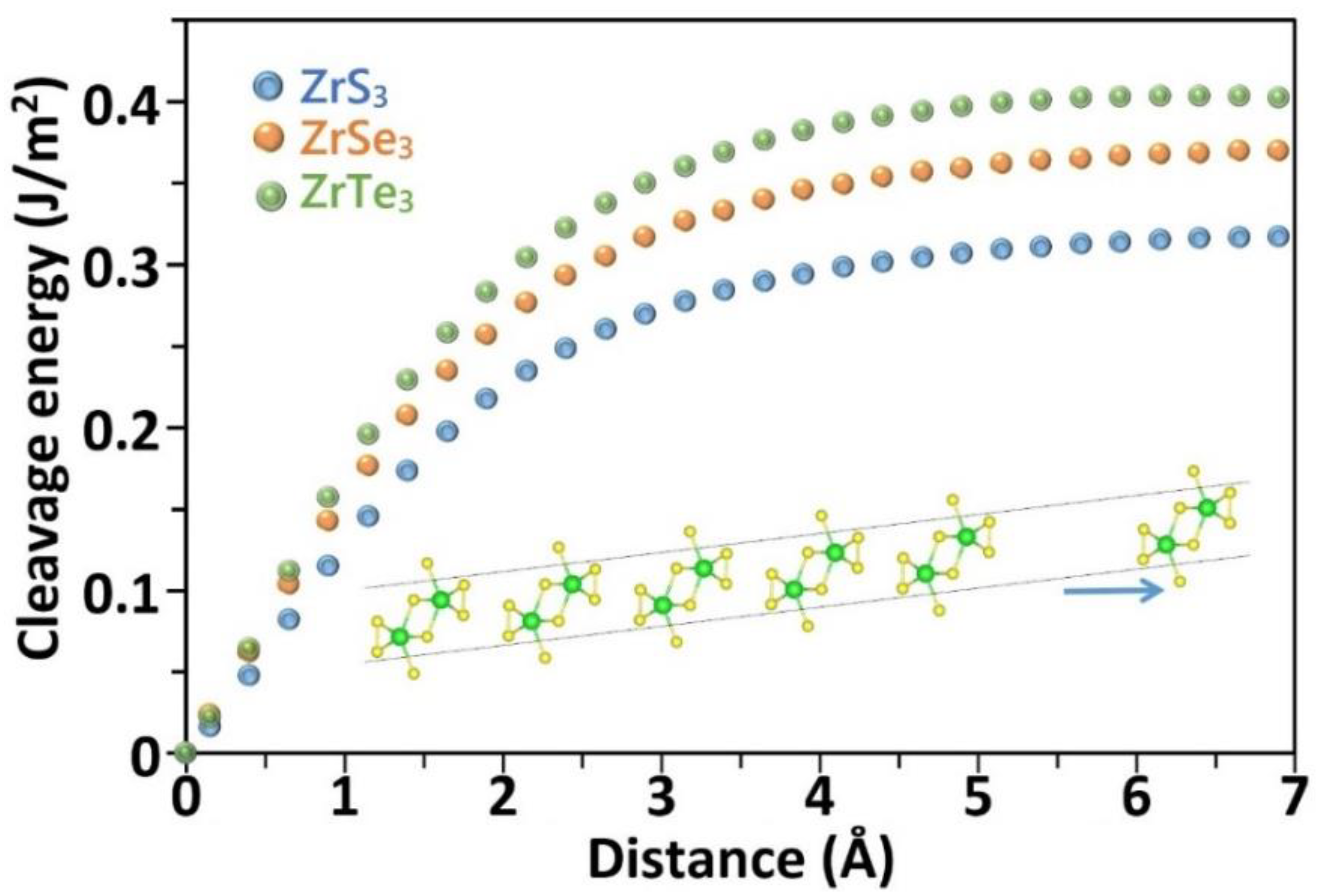
3. Results and Discussion

Figure 1 depicts different views of the crystal structure of the ZrX3 (X = S, Se, Te) monolayers. According to Figure 1, a ZrX3 monolayer includes a rectangular primitive unit cell with a P21/M (No. 11) space group and highly anisotropic atomic arrangement along the x and y directions. A ZrX3 monolayer can basically be considered laterally aligned (along the x direction) and alternatively inverted triangular prismatic ZrX3 chains, which are connected through Zr-X bonds in the zx plane ( l Z r X a ). The inter-chain Zr-X bonds ( l Zr X a ) were found to be longer than the Zr-X bonds within the chain ( l Zr X b ). This observation was expected to lead to anisotropic mechanical, optical, and electronic properties in the ZrX3 monolayers. Table 1 summarizes the optimized lattice constants, bond lengths, and calculated band gap properties of each ZrX3 monolayer. Our predicted lattice constants for ZrX3 monolayers agree well with previous data: a = 5.138 Å and b = 3.619 Å for ZrS3, a = 5.423 Å and b = 3.745 Å for ZrSe3, and a = 5.942 Å and b = 3.909 Å for ZrTe3 [12]. For the bulk structures the box size along the out-of-plane direction for the ZrS3, ZrSe3, and ZrTe3 monolayers were found to be 9.01, 9.46, and 10.14 Å, respectively, with excellent agreement with corresponding experimental values of 8.98 [24], 9.43 [24], and 10.10 Å [24], respectively. In the Supplementary Materials document, the complete crystal data for the single-layer and bulk ZrX3 systems are given. According to spin-polarized calculations, we found that these systems are not magnetic. Looking carefully to the crystal structure of a ZrX3 monolayer, two different types of X atoms can be identified: surface X atoms, which exist in pairs (X2), and the internal ones, which contribute to the inter-chain binding and only coordinate with the Zr atom. Our calculated bond lengths for X2 were 2.07, 2.38, and 2.83 Å, which are only slightly different than the typical values for single covalent S-S, Se-Se, and Te-Te bonds [25,26]. According to Bader charge analysis, Zr atoms are positively charged and transfer electrons to the surface and internal chalcogen X atoms, indicating that electrostatic interactions play a key role in keeping the structural integrity of ZrX3 monolayers. The amount of charge exchange decreased as the electronegativity of chalcogen X atoms decreased: 1.77 e for ZrS3, 1.61 e for ZrSe3, and 1.33 e for ZrTes3. Although all chalcogen atoms were negatively charged, it was found that surface X atoms yielded almost twice the charge as those of the internal counterparts. The electron localization pattern along the Zr-X bonds shown in Figure 1b also supports the idea of the dominance of ionic interaction within the ZrX3 monolayers. The electron localization maps also show the gradual increase in electron localization in between adjacent surface X2 moieties from ZrS3 to ZrTe3 monolayers. For the case of ZrTe3, an appreciable electron localization was found in between adjacent surface Te2 moieties (find Figure 1d), indicating interactions between them. It is worth noting that our calculated distance between surface Te2 moieties in the ZrTe3 monolayer was 3.05 Å, which is only slightly larger than Te-Te bonds calculated for experimentally synthesized 2D α- and β-Te: 3.02 Å [27]. Therefore, surface Te2 moieties in the ZrTe3 monolayer can actually be considered infinite Te2 chains extended along the x direction. In other words, by comparing the ELF contours for the over-surface non-bonded X-X bonds, around the center of the Te-Te pairs (Figure 1d), the ELF values were considerably higher than those in the corresponding S-S (Figure 1b) and Se-Se (Figure 1c) pairs, which reveals the formation of stronger Te-Te interactions in the ZrTe3 monolayer.
After an effective analysis of the structural and bonding characteristics of the ZrX3 monolayers, we next examined their dynamic stability by evaluating phonon dispersion relations. The predicted phonon dispersion along highly symmetrical points for the ZrS3, ZrSe3, and ZrTe3 monolayers are illustrated in Figure 2. As the first important finding, the phonon modes were free of imaginary frequencies, confirming the dynamic stability of these systems. By increasing the atomic number of chalcogen atoms in the ZrX3 nanosheets, it was clear that although preserving the general form of dispersions, the phonon modes showed narrower frequency ranges, which indicates lower group velocity. It is noticeable that all acoustic and optical modes appeared with considerable intersections, stimulating the scattering and reducing the lifetime for modes with higher frequencies. With generally lower group velocity and lifetime, it was expected that by increasing the atomic number of chalcogen atoms in ZrX3 nanosheets, they would show lower lattice thermal conductivity, which is consistent with recent theoretical results for the ZrS3 [13] and ZrTe3 [14] systems.
The Raman spectrum of each ZrX3 monolayer is shown in Figure 3. Apparently, due to the same crystal symmetry of each monolayer ZrX3, the number of Raman active modes was the same in all structures. It is seen that there existed three prominent Raman active phonon modes for each monolayer structure. The three prominent peaks are labeled I, II, and III, as shown in the figure. As the chalcogenide atom changed from S to Te, which means the atomic radius increased, the frequency of each prominent peak displayed red shift due to the larger atomic mass. In addition, the motion of individual atoms showing the vibration of the corresponding phonon mode is also given in the right panel of the figure. The phonon mode I was calculated to be at the frequencies 522, 292, and 151 cm−1 for ZrS3, ZrSe3, and ZrTe3 monolayers, respectively. Apparently, mode I arose from the in-plane vibration of the outermost chalcogenide atoms against each other. On the other hand, modes II and III stemmed from the out-of-plane vibration of the Zr and chalcogenide atoms. The frequencies of modes II/III were calculated to be 321/274, 220/171, and 74/62 cm−1 for the ZrS3, ZrSe3, and ZrTe3 monolayers, respectively. The mode II phonon represents the out-of-plane vibration of the internal chalcogenide atoms against Zr atoms, whereas the outermost chalcogenide atoms made little contribution to the vibration. Finally, the mode III phonon arose from the out-of-phase vibration of each atomic level with respect to each other, that is, the outermost chalcogenide atoms vibrated against each other, and Zr atoms also moved out of phase. The three characteristic phonon peaks were quite important for the detection of the ZrX3 monolayers.
Worth mentioning is that to prepare 2D materials, the common approaches include mechanical exfoliation, chemical vapor deposition (CVD), and liquid-phase exfoliation. The mechanical exfoliation of bulk 2D materials into single or multiple layers can be achieved by using external driving forces [28,29,30]. Before analyzing the electronic properties, it is thus very useful to investigate the mechanical exfoliation energy required for the isolation of the ZrS3, ZrSe3, and ZrTe3 monolayers from their native bulk structures. For this purpose, we first acquired the energy-minimized six-layer slabs of the ZrX3 nanosheets, with the same stacking pattern as that of their bulk systems. In the next step, the last layer was steadily separated toward the out-of-plane vacuum direction, with a small step of 0.25 Å. The change in the energy of the systems was subsequently calculated and the cleavage energy was recorded. As shown in Figure 4, the relative energies showed sharp initial increases and later reach converged values. According to our DFT-D3 simulations, the exfoliation energies of 0.32, 0.37, and 0.40 J/m2 were predicted for the isolation of the ZrS3, ZrSe3, and ZrTe3 monolayers, which are comparable to that of graphene: 0.37 J/m2 [31]. These findings reveal that the separate layers in these systems showed relatively weak interactions and moreover highlight that by increasing the atomic number of chalcogen atoms, the exfoliation energy increased, consistent with earlier studies [32]. We remind that Li et al. [12] synthesized ZrSe3 nanosheets via the mechanical exfoliation method. Taking into account our predictions for the exfoliation energies and the aforementioned experimental achievement, the experimental isolation of ZrS3 and ZrTe3 monolayers from their bulk structures is very bright.
To explore the electronic characteristics of the ZrX3 monolayers, we calculated electronic band structures using PBE and the more accurate HSE06 functional. The effect of spin-orbit coupling (SOC) on band gap properties of ZrX3 monolayers was also examined. Figure 5 depicts the HSE06 band structures of the ZrX3 monolayers without and with the inclusion of SOC effects. The corresponding PBE results are also given in Figure S1 in the Supplementary Materials. Band-gap values as well as transition k-points for HSE06 results are listed in Table 1. According to results shown in Figure 5 and Table 1, the ZrS3 and ZrSe3 monolayers were indirect gap semiconductors with HSE06 band gaps of 1.93 and 1.01 eV. In the ZrS3 monolayer, VBM was located at a k-point on the Γ-X path (0.184210 k 1 + 0 k 2 , k 1 and k 2 are lattice vectors of reciprocal space) and CBM was located at the Γ point. The direct gap at the Γ point in ZrS3 was only 0.08 eV larger than the indirect gap, indicating that ZrS3 may behave as a quasi-direct gap semiconductor. VBM and CBM in the ZrSe3 monolayers, were, however, located at the Γ and X points, respectively. Both band gap values and transition k-points are in good agreement with previous data (1.92 eV for ZrS3 and 0.92 eV for ZrSe3) [33]. It can be seen that for each of the ZrS3 and ZrSe3 monolayers, PBE and HSE06 band structures looked similar, except the PBE band gaps, as expected, were underestimated. It was also observed that the inclusion of SOC did not yield a detectable effect on the band structure of the ZrSe3, but it reduced the HSE06 (PBE) band gap of the ZrSe3 monolayer by 0.08 (0.06) eV (find Figure 5 and Figure S1). Unlike the ZrS3 and ZrSe3 monolayers, the ZrTe3 monolayer exhibited a metallic character irrespective of the functional used, which is also in agreement with a previous report [33].
In order to further rationalize the band-gap change trend in ZrX3 monolayers, for each one, we calculated atom-type projected density of states (PDOS) and charge density distributions of valance band maximum (VBM) and conduction band minimum (CBM), as shown in Figure 5. For the three monolayers, VBM was mainly contributed by internal X-(py,pz) with a minor contribution from Zr-(py,dyz,dxy), representing a shallow bonding s(Zr-X) state. Considering the fact that the energy position of p orbitals of chalcogen X atom increased from S to Te, VBM in the ZrX3 monolayers was expected to move upward in energy from the ZrS3 to ZrTe3 monolayer. This expectation was confirmed by the absolute energy positions of VBMs of the ZrS3, ZrSe3, and ZrTe3 monolayers, calculated to be −6.57, −5.68, and −5.21 eV, respectively. CBM in the ZrS3 lattice was made of Zr-(s, d z 2 , d x 2 y 2 ), representing a bonding (Zr-Zr) state propagating along the y direction. The charge densities of CBMs in the ZrSe3 and ZrTe3 monolayers were, however, almost exclusively distributed over surface X2 moieties, and they both represented bonding (X-X) states made of X-(s,px,pz). As our electron localization analysis revealed, the strengths of interaction between adjacent X2 moiety increased from ZrS3 to ZrTe3. The stronger the interaction between X2 moieties, the lower the absolute energy position. Putting the conclusions together, from ZrS3 to ZrTe3, VBM shifted upward in energy whereas CBM shifted downward, leading to smaller band gaps (Eg(ZrS3) > Eg(ZrSe3) > Eg(ZrTe3)).
Finally, we examined the mechanical responses by performing uniaxial tensile simulations along the x and y directions, as distinguished in Figure 1. Uniaxial stress–strain responses of the ZrX3 monolayers along the x and y directions are illustrated in Figure 6. In these results, real volumes of the deformed lattices were considered in the conversion of the stress values to the standard GPa unit [34,35,36]. The real area of the deformed nanosheets can be obtained using the simulation box sizes along the in-plane directions. The real volume at every strain was calculated by finding the normal distance between boundary chalcogen atoms plus their effective vdW diameter. According to our geometry-optimized bulk lattices, the thicknesses of the stress-free ZrS3, ZrSe3, and ZrTe3 monolayers were predicted to be 9.01, 9.46, and 10.14 Å, respectively, equivalent to the effective vdW dimeters of 3.05, 3.20, and 3.26 Å for the S, Se, and Te atoms in the ZrX3 monolayers, respectively. The stress–strain curves plotted in Figure 6 are uniaxial, which means that during the complete deformation and after the geometry minimization, these kagome monolayers exhibited a stress component only along the loading direction and showed negligible values along the two other perpendicular directions. As expected, and stemming from the anisotropic structure, the stress–strain curves along the x and y directions were considerably different, confirming highly anisotropic mechanical features. The elastic modulus of ZrS3, ZrSe3, and ZrTe3 monolayers along the x (y) directions were predicted to be 93 (142), 90 (118), and 120(56) GPa, respectively. The ultimate tensile strength of the ZrS3, ZrSe3, and ZrTe3 monolayers along the x (y) directions were predicted to be 6.2 (16.5), 4.9 (17.4), and 4.6 (11.8) GPa, respectively. As expected, due to the existence of more connecting bonds along the y direction than the x counterpart, these systems showed considerably higher tensile strength along this direction. The same observation is also consistent for the elastic modulus of the ZrS3 and ZrSe3 monolayers. The ZrSe3 monolayers unexpectedly showed a higher elastic modulus along the x direction, which, as discussed earlier with the ELF results, was due to the formation of continuous over-surface Te-Te interactions along this direction in this system. As is clear, due to the multifaceted structural and bonding effects, the ZrX3 nanosheets showed highly anisotropic and complex mechanical behavior. Worthy to mention that complex material properties can be explored using MTPs with high accuracy and accelerated computational costs [37,38,39,40,41].

4. Concluding Remarks

We studied the structural, phononic, electronic, and single-layer exfoliation energies and mechanical properties of ZrX3 (X = S, Se, Te) monolayers. The acquired phonon dispersion relations revealed the dynamical stability of the aforementioned 2D systems. Exfoliation energies of 0.32, 0.37, and 0.40 J/m2 were predicted for the ZrS3, ZrSe3, and ZrTe3 monolayers’ isolation, which confirms bright prospects for the mechanical isolation of ZrS3 and ZrTe3 monolayers from their native bulk structures. ZrS3 and ZrSe3 monolayers were found to be indirect gap semiconductors, with HSE06 band gaps of 1.93 and 1.01 eV, whereas the ZrTe3 monolayer yielded a metallic character. The elastic modulus of ZrS3, ZrSe3, and ZrTe3 monolayers along the x (y) directions were predicted to be 93 (142), 90 (118), and 120(56) GPa, respectively, and the corresponding ultimate tensile strength values were found to be 6.2 (16.5), 4.9 (17.4), and 4.6 (11.8) GPa, respectively. It is shown that because of multifaceted structural and bonding effects, ZrX3 nanosheets showed highly anisotropic and complex mechanical behavior. The presented DFT results provide an effective overview of the key physical properties of the ZrX3 (X = S, Se, Te) nanosheets, which can serve as valuable information for their practical application in nanodevices.

Supplementary Materials

The following supporting information can be downloaded at: https://www.mdpi.com/article/10.3390/en15155479/s1, Figure S1: PBE band structures of the ZrX3 monolayers without (purple solid lines) and with (red solid line) the inclusion of SOC effects.

Author Contributions

Conceptualization, B.M. and M.M.; Data curation, B.M., F.S. and M.Y.; Methodology, B.M., F.S. and M.Y.; Writing—original draft preparation, B.M., F.S. and M.Y.; Funding acquisition, X.Z. All authors have read and agreed to the published version of the manuscript.

Funding

This research was funded by Deutsche Forschungsgemeinschaft (DFG, German Research Foundation) under Germany’s Excellence Strategy within the Cluster of Excellence PhoenixD (EXC 2122, Project ID 390833453). This work was partially supported by the BAGEP Award of the Science Academy with funding supplied by the Sevinc-Erdal Inonu Foundation.

Institutional Review Board Statement

Not applicable.

Informed Consent Statement

Not applicable.

Data Availability Statement

The data presented in this study are available on request from the corresponding author.

Acknowledgments

F.S. thanks the Persian Gulf University Research Council, Iran, for the support of this study. B.M. is thankful to the VEGAS cluster at Bauhaus University of Weimar for providing the computational resources. Computational resources were partially provided by TUBITAKULAKBIM, High Performance and Grid Computing Center (TR-Grid e-Infrastructure).

Conflicts of Interest

The authors have no conflict of interest to declare that are relevant to the content of this article.

References

  1. Novoselov, K.S.; Geim, A.K.; Morozov, S.V.; Jiang, D.; Zhang, Y.; Dubonos, S.V.; Grigorieva, I.V.; Firsov, A.A. Electric field effect in atomically thin carbon films. Science 2004, 306, 666–669. [Google Scholar] [CrossRef] [PubMed] [Green Version]
  2. Geim, A.K.; Novoselov, K.S. The rise of graphene. Nat. Mater. 2007, 6, 183–191. [Google Scholar] [CrossRef] [PubMed]
  3. Castro Neto, A.H.; Peres, N.M.R.; Novoselov, K.S.; Geim, A.K.; Guinea, F. The electronic properties of graphene. Rev. Mod. Phys. 2009, 81, 109–162. [Google Scholar] [CrossRef] [Green Version]
  4. Hong, Y.-L.; Liu, Z.; Wang, L.; Zhou, T.; Ma, W.; Xu, C.; Feng, S.; Chen, L.; Chen, M.-L.; Sun, D.-M.; et al. Chemical vapor deposition of layered two-dimensional MoSi2N4 materials. Science 2020, 369, 670–674. [Google Scholar] [CrossRef]
  5. Novoselov, K.S. Discovery of 2D van der Waals layered MoSi2N4 family. Natl. Sci. Rev. 2020, 7, 1842–1844. [Google Scholar] [CrossRef]
  6. Bakharev, P.V.; Huang, M.; Saxena, M.; Lee, S.W.; Joo, S.H.; Park, S.O.; Dong, J.; Camacho-Mojica, D.C.; Jin, S.; Kwon, Y.; et al. Chemically induced transformation of chemical vapour deposition grown bilayer graphene into fluorinated single-layer diamond. Nat. Nanotechnol. 2020, 15, 59–66. [Google Scholar] [CrossRef] [Green Version]
  7. Li, P.; Zhang, J.; Zhu, C.; Shen, W.; Hu, C.; Fu, W.; Yan, L.; Zhou, L.; Zheng, L.; Lei, H.; et al. Penta-PdPSe: A New 2D Pentagonal Material with Highly In-Plane Optical, Electronic, and Optoelectronic Anisotropy. Adv. Mater. 2021, 33, 2102541. [Google Scholar] [CrossRef]
  8. Fang, Y.; Wang, F.; Wang, R.; Zhai, T.; Huang, F. 2D NbOI2: A Chiral Semiconductor with Highly In-Plane Anisotropic Electrical and Optical Properties. Adv. Mater. 2021, 33, 2101505. [Google Scholar] [CrossRef] [PubMed]
  9. Wang, X.; Xiong, T.; Zhao, K.; Zhou, Z.; Xin, K.; Deng, H.-X.; Kang, J.; Yang, J.; Liu, Y.-Y.; Wei, Z. Polarimetric Image Sensor and Fermi Level Shifting Induced Multi-Channel Transition Based on Two-dimensional PdPS. Adv. Mater. 2021, 33, 2107206. [Google Scholar] [CrossRef]
  10. Seo, T.H.; Lee, W.; Lee, K.S.; Hwang, J.Y.; Son, D.I.; Ahn, S.; Cho, H.; Kim, M.J. Dominant formation of h-BC2N in h-BxCyNz films: CVD synthesis and characterization. Carbon N. Y. 2021, 182, 791–798. [Google Scholar] [CrossRef]
  11. Bykov, M.; Bykova, E.; Ponomareva, A.V.; Tasnádi, F.; Chariton, S.; Prakapenka, V.B.; Glazyrin, K.; Smith, J.S.; Mahmood, M.F.; Abrikosov, I.A.; et al. Realization of an Ideal Cairo Tessellation in Nickel Diazenide NiN2: High-Pressure Route to Pentagonal 2D Materials. ACS Nano 2021, 15, 13539–13546. [Google Scholar] [CrossRef] [PubMed]
  12. Li, H.; Sanchez-Santolino, G.; Puebla, S.; Frisenda, R.; Al-Enizi, A.M.; Nafady, A.; D’Agosta, R.; Castellanos-Gomez, A. Strongly Anisotropic Strain-Tunability of Excitons in Exfoliated ZrSe3. Adv. Mater. 2022, 34, 2103571. [Google Scholar] [CrossRef] [PubMed]
  13. Wang, C.; Zheng, C.; Gao, G. Bulk and Monolayer ZrS3 as Promising Anisotropic Thermoelectric Materials: A Comparative Study. J. Phys. Chem. C 2020, 124, 6536–6543. [Google Scholar] [CrossRef]
  14. Debnath, T.; Debnath, B.; Lake, R.K. Thermal conductivity of the quasi-one-dimensional materials TaSe3 and ZrTe3. Phys. Rev. Mater. 2021, 5, 34010. [Google Scholar] [CrossRef]
  15. Kresse, G.; Furthmüller, J. Efficient iterative schemes for ab initio total-energy calculations using a plane-wave basis set. Phys. Rev. B 1996, 54, 11169–11186. [Google Scholar] [CrossRef]
  16. Perdew, J.P.; Burke, K.; Ernzerhof, M. Generalized Gradient Approximation Made Simple. Phys. Rev. Lett. 1996, 77, 3865–3868. [Google Scholar] [CrossRef] [Green Version]
  17. Grimme, S.; Antony, J.; Ehrlich, S.; Krieg, H. A consistent and accurate ab initio parametrization of density functional dispersion correction (DFT-D) for the 94 elements H-Pu. J. Chem. Phys. 2010, 132, 154104. [Google Scholar] [CrossRef] [Green Version]
  18. Kresse, G.; Hafner, J. Ab initio molecular dynamics for liquid metals. Phys. Rev. B 1993, 47, 558–561. [Google Scholar] [CrossRef]
  19. Monkhorst, H.; Pack, J. Special points for Brillouin zone integrations. Phys. Rev. B 1976, 13, 5188–5192. [Google Scholar] [CrossRef]
  20. Shapeev, A.V. Moment tensor potentials: A class of systematically improvable interatomic potentials. Multiscale Model. Simul. 2016, 14, 1153–1173. [Google Scholar] [CrossRef]
  21. Mortazavi, B.; Shojaei, F.; Javvaji, B.; Rabczuk, T.; Zhuang, X. Outstandingly high thermal conductivity, elastic modulus, carrier mobility and piezoelectricity in two-dimensional semiconducting CrC2N4: A first-principles study. Mater. Today Energy 2021, 22, 100839. [Google Scholar] [CrossRef]
  22. Togo, A.; Tanaka, I. First principles phonon calculations in materials science. Scr. Mater. 2015, 108, 1–5. [Google Scholar] [CrossRef] [Green Version]
  23. Mortazavi, B.; Novikov, I.S.; Podryabinkin, E.V.; Roche, S.; Rabczuk, T.; Shapeev, A.V.; Zhuang, X. Exploring phononic properties of two-dimensional materials using machine learning interatomic potentials. Appl. Mater. Today 2020, 20, 100685. [Google Scholar] [CrossRef]
  24. Brattas, L.; Kjekshus, A. Others Properties of compounds with zrse 3-type structure. Acta Chem. Scand. 1972, 26, 3441–3449. [Google Scholar] [CrossRef]
  25. Zhang, H.; Wang, J.; Guégan, F.; Yu, S.; Frapper, G. Prediction of allotropes of tellurium with molecular, one- and two-dimensional covalent nets for photofunctional applications. RSC Adv. 2021, 11, 29965–29975. [Google Scholar] [CrossRef]
  26. Tareen, A.K.; Khan, K.; Aslam, M.; Zhang, H.; Liu, X. Recent progress, challenges, and prospects in emerging group-VIA Xenes: Synthesis, properties and novel applications. Nanoscale 2021, 13, 510–552. [Google Scholar] [CrossRef]
  27. Zhu, Z.; Cai, X.; Yi, S.; Chen, J.; Dai, Y.; Niu, C.; Guo, Z.; Xie, M.; Liu, F.; Cho, J.-H.; et al. Multivalency-Driven Formation of Te-Based Monolayer Materials: A Combined First-Principles and Experimental study. Phys. Rev. Lett. 2017, 119, 106101. [Google Scholar] [CrossRef] [Green Version]
  28. Le, T.-H.; Oh, Y.; Kim, H.; Yoon, H. Exfoliation of 2D Materials for Energy and Environmental Applications. Chem. Eur. J. 2020, 26, 6360–6401. [Google Scholar] [CrossRef]
  29. Huo, C.; Yan, Z.; Song, X.; Zeng, H. 2D materials via liquid exfoliation: A review on fabrication and applications. Sci. Bull. 2015, 60, 1994–2008. [Google Scholar] [CrossRef]
  30. Biccai, S.; Barwich, S.; Boland, D.; Harvey, A.; Hanlon, D.; McEvoy, N.; Coleman, J.N. Exfoliation of 2D materials by high shear mixing. 2D Mater. 2018, 6, 15008. [Google Scholar] [CrossRef]
  31. Wang, W.; Dai, S.; Li, X.; Yang, J.; Srolovitz, D.J.; Zheng, Q. Measurement of the cleavage energy of graphite. Nat. Commun. 2015, 6, 7853. [Google Scholar] [CrossRef] [PubMed] [Green Version]
  32. Raeisi, M.; Mortazavi, B.; Podryabinkin, E.V.; Shojaei, F.; Zhuang, X.; Shapeev, A. V High Thermal Conductivity in Semiconducting Janus and Non-Janus Diamanes. Carbon N. Y. 2020, 167, 51–61. [Google Scholar] [CrossRef]
  33. Li, M.; Dai, J.; Zeng, X.C. Tuning the electronic properties of transition-metal trichalcogenides via tensile strain. Nanoscale 2015, 7, 15385–15391. [Google Scholar] [CrossRef] [PubMed] [Green Version]
  34. Zarghami Dehaghani, M.; Molaei, F.; Spitas, C.; Hamed Mashhadzadeh, A. Thermal rectification in nozzle-like graphene/boron nitride nanoribbons: A molecular dynamics simulation. Comput. Mater. Sci. 2022, 207, 111320. [Google Scholar] [CrossRef]
  35. Dadrasi, A.; Albooyeh, A.; Fooladpanjeh, S.; Salmankhani, A.; Hamed Mashhadzadeh, A.; Saeb, M.R. Theoretical examination of the fracture behavior of BC3 polycrystalline nanosheets: Effect of crack size and temperature. Mech. Mater. 2022, 165, 104158. [Google Scholar] [CrossRef]
  36. Farzadian, O.; Dehaghani, M.Z.; Kostas, K.V.; Mashhadzadeh, A.H.; Spitas, C. A theoretical insight into phonon heat transport in graphene/biphenylene superlattice nanoribbons: A molecular dynamic study. Nanotechnology 2022, 33, 355705. [Google Scholar] [CrossRef]
  37. Mortazavi, B. Ultrahigh Thermal Conductivity and Strength in Direct-Gap Semiconducting Graphene-like BC6N: A First-Principles and Classical Investigation. Carbon N. Y. 2021, 182, 373–383. [Google Scholar] [CrossRef]
  38. Mortazavi, B.; Silani, M.; Podryabinkin, E.V.; Rabczuk, T.; Zhuang, X.; Shapeev, A. V First-Principles Multiscale Modeling of Mechanical Properties in Graphene/Borophene Heterostructures Empowered by Machine-Learning Interatomic Potentials. Adv. Mater. 2021, 33, 2102807. [Google Scholar] [CrossRef]
  39. Mortazavi, B.; Podryabinkin, E.V.; Roche, S.; Rabczuk, T.; Zhuang, X.; Shapeev, A. V Machine-Learning Interatomic Potentials Enable First-Principles Multiscale Modeling of Lattice Thermal Conductivity in Graphene/Borophene Heterostructures. Mater. Horizons 2020, 7, 2359–2367. [Google Scholar] [CrossRef]
  40. Arabha, S.; Rajabpour, A. Thermo-Mechanical Properties of Nitrogenated Holey Graphene (C2N): A Comparison of Machine-Learning-Based and Classical Interatomic Potentials. Int. J. Heat Mass Transf. 2021, 178, 121589. [Google Scholar] [CrossRef]
  41. Arabha, S.; Aghbolagh, Z.S.; Ghorbani, K.; Hatam-Lee, M.; Rajabpour, A. Recent Advances in Lattice Thermal Conductivity Calculation Using Machine-Learning Interatomic Potentials. J. Appl. Phys. 2021, 130, 210903. [Google Scholar] [CrossRef]
Figure 1. (a) Crystal structure of the ZrX3(X = S, Se, Te) monolayers. The primitive cell, first Brillouin zone, a prismatic chain of ZrX3 (red dashed-line rectangle), surface X2 moieties, and Zr-X bonds in zx and zy planes ( l Z r X a , l Z r X b ) are also distinguished. (bd) Contour maps of electron localization function (ELF) for the ZrX3 monolayers. The regions in between surface X2 moieties are shown by red dashed-line ellipses. In this figure, green, yellow, orange, and dark yellow circles indicate Zr, S, Se, and Te atoms, respectively.
Energies 15 05479 g001
Figure 2. Phonon dispersion relations of the ZrS3, ZrSe3, and ZrTe3 monolayers.
Energies 15 05479 g002
Figure 3. The Raman spectrum of each monolayer ZrX3 structure (on the left) and the vibrational characteristic of the individual atoms for the most prominent Raman active modes (on the right).
Energies 15 05479 g003
Figure 4. Cleavage energy of the ZrS3, ZrSe3, and ZrTe3 monolayers as a function of separation distance.
Energies 15 05479 g004
Figure 5. HSE06 band structures of ZrX3 monolayers without (purple solid lines) and with (red solid line) the inclusion of SOC effects. Next to the band structures are the HSE06 calculated atom-type projected density of states. For ZrS3 and ZrSe3, charge density distributions of their VBMs and CBMs are also shown. For ZrTe3 that exhibits a metallic character, charge density distributions at two k-points below and above (−0.02 < EK − EFermi < 0.02 eV) its Fermi level are shown. For both ZrS3 and ZrSe3, VBM of HSE06 + SOC calculation is set to 0 and HSE06 band energies are aligned using vacuum-level calculations.
Energies 15 05479 g005
Figure 6. True uniaxial stress–strain relations of the (a) ZrS3, (b) ZrSe3, and (c) ZrTe3 monolayers elongated along the y and x directions.
Energies 15 05479 g006
Table 1. Structural and electronic properties of ZrX3 (X = S, Se, Te) monolayers.
Latticea,b (Å) 1 l Z r X a ,   l Z r X b   ( Å )   2 l X X i n t r a   ( Å )   3 l X X i n t e r   ( Å )   4 Q(Zr,Xsurface,Xinternal) (e) 5 E g P B E / E g P B E + S O C /   E g H S E 06 / E g H S E 06 + S O C ( eV )   6
ZrS35.13,3.632.72, 2.612.073.061.77,−0.41,−0.951.06/1.06/1.93 (Γ-X)→Γ/1.93
ZrSe35.41,3.762.87, 2.742.383.031.61,−0.38,−0.850.33/0.27/1.01 Γ→X/0.93
ZrTe35.89,3.923.16, 2.982.833.051.33,−0.34,−0.64Metal/Metal/Metal/Metal
1 PBE optimized lattice parameters along x and y directions, respectively (Figure 1). 2 Bond lengths of those Zr-X bonds that are in the xz and yz planes, respectively (Figure 1). 3 Bond length of covalently bonded X2 moieties (Figure 1). 4 Distance between adjacent X2 moieties. 5 Average Bader charges on each of the Zr atoms, X atoms of X2 moieties (Xsurface), and internal X atoms (Xinternal), respectively (Figure 1). 6 Band gaps using PBE functional ( E g P B E )/PBE functional with inclusion of spin-orbit coupling (SOC) effect/ HSE06 functional ( E g H S E 06 )/HSE06 functional with inclusion of SOC effects ( E g H S E 06 + S O C ). For ZrS3 and ZrSe3, K-points at which valance band maximum and conduction band minimum occurs are shown in parentheses.
Publisher’s Note: MDPI stays neutral with regard to jurisdictional claims in published maps and institutional affiliations.

