1. Introduction
In response to increasing photovoltaic (PV) penetration levels on the grid, distributed energy resource (DER) devices—e.g., photovoltaic inverters and energy storage systems (ESS)—are now required to include control modes to improve power quality, in accordance with the U.S. interconnection standard, IEEE 1547-2018 [
1]. The set of control modes stipulated in IEEE 1547 includes fixed power factor, voltage-reactive power mode, and an active power limit, providing grid operators with new ways to support distribution voltages [
2], participate in load-generation balancing [
3], and stabilize the system during power system faults [
4].
While the impact of advanced inverter functionality on grid stability and power quality has been well studied [
5], the impact of this behavior on inverter lifetime and reliability has not. Operating at off-nominal operating conditions (e.g., non-unity power factor) has been shown to increase switch loss and thermal loss, accelerate device degradation, and reduce overall system lifetime [
6,
7,
8,
9]. There is a clear tradeoff between PV inverter reliability and grid-level advantages in reliability and power quality for advanced inverter operation.
This also raises major financial and equity questions when grid operators, aggregators, and other third parties operate DER equipment in grid-support modes. Currently, customers are not compensated for reactive power, but reactive power operating modes are potentially reducing the lifetime of their equipment. Additionally, when using voltage-reactive power modes, depending on the customer’s geographic location on a distribution feeder, their DER equipment is likely to operate further from unity power factor (and more often) compared with a customer located closer to the feeder substation. As a result, certain customers are sacrificing more DER lifetime than others to help grid operators perform voltage regulation operations. These issues cannot be resolved through regulations, utility incentives, or compensation without fully understanding the impacts on the DER equipment. This work is a first step in addressing these challenges by quantifying the disparity between DER lifetimes when operating under different reactive power modes.
However, significant barriers exist in quantifying this reduction in unit lifetime using component-level stresses. The first difficulty is instrumenting and monitoring switch stress across the inverter’s entire active and reactive power operating envelope. The other is determining the appropriate failure model and lifetime profiles to estimate lifetime reductions.
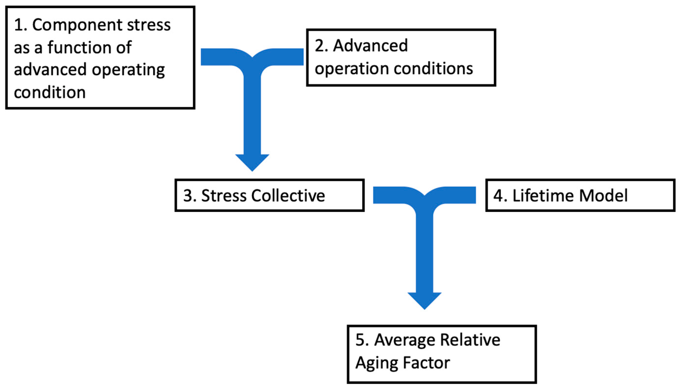
In this work, we address the first of those challenges and describe a framework for instrumenting and autonomously measuring inverter component stress for a variety of different advanced inverter operating conditions (
Figure 1). We demonstrate how those measurements (Step 1) can then be coupled with appropriate advanced inverter operating conditions (either real or expected, Step 2) to create a stress collective (Step 3) [
10]. This stress collective can then be combined with an appropriate component lifetime model (Step 4) to determine an effective reduction in useful life of the inverter, due to advanced inverter functionality (Step 5). The primary contributions of this work include (a) creating and demonstrating a flexible framework to model lifetime reductions of DER equipment under different grid-support operating scenarios acording to measured component-level stresses, and (b) evaluations of switch and capacitor stress under reactive power modes.
The remainder of the paper is structured as follows.
Section 2 discusses the laboratory setup for extracting component loss maps as a function of advanced inverter operation;
Section 3 presents the loss mapping of three inverters and discusses the meaning of the results; and
Section 4 couples the experimental data with component lifetime models to calculate an example reduction in inverter lifetime due to advanced inverter functionality;
Section 5 concludes the paper with the importance of the findings and suggested future work.
2. Component Stress Measurements
The first step of the framework shown in
Figure 1 is the measurement of component stresses as a function of advanced operating condition. To ensure an accurate parameterization, component stress must be measured under a wide range of advanced operating conditions. This process can be very long and tedious if performed manually. To automate this process, we altered the System Validation Platform (SVP) [
11], which was originally developed as a flexible framework to measure autonomously system-level inverter operations for certification processes. The SVP framework was altered to measure, process, and store component-level loss maps, which can be used as the basis to calculate inverter lifetime reductions as a function of advanced inverter operating condition. Similar in situ approaches could be employed by inverter manufacturers as prognostics tools to calculate component damage, model lifetime, and dynamically calculate time-of-use prices for grid-support functions based on inverter lifetime costs.
2.1. Data Collection
The open-source System Validation Platform (SVP) was initially developed under a Cooperative Research and Development Agreement (CRADA) between Sandia National Laboratories and SunSpec Alliance [
11]. This platform has since been expanded by the Smart Grid International Research Facility Network (SIRFN) to include a range of equipment drivers and test scripts for conducting DER interoperability and electrical characterization experiments. The SVP has been used to evaluate test procedures defined in IEEE 1547.1 [
12], Underwriters Laboratories 1741 Supplement A [
13], a test protocol for IEC TR 61850-90-7 [
14], as well as to collect extensive grid-support function operational data to model DER operations [
15]. The software platform was written in Python and includes the ability to script actions for multiple hardware devices using a library of device drivers and abstraction layers. Abstraction layers and drivers have been created for PV simulators, grid simulators, DER, data acquisition systems, load banks, and switches [
16]. This architecture allows the same test logic (SVP scripts) to be run at multiple laboratories with different equipment.
The SVP allowed flexible measurement of any accessible component inside the inverter, including switches, capacitors, inductors, etc. Using this open architecture as a starting place, a new Tektronix oscilloscope driver and reliability script were created to measure component losses (
Figure 2). An SVP script automated the loss calculations for a range of PV irradiance values and power factors, to produce inverter component loss maps under different operating conditions. The SVP was run on a Windows 10 computer networked to the inverters, PV simulator, and Tektronix data acquisition system (DAS). Maps were created for two single-phase inverters and one three-phase.
2.2. Switch Loss Measurements
In the first experiment, an SVP script measured the switching losses of an inverter by recording switch voltage and current during system operation, as depicted in
Figure 2. The inverter tested had a 4-switch H-bridge configuration operating with a variable duty cycle PWM with a frequency ~70 kHz. One of the constituent MOSFETs was monitored using a PEM Ltd. CWT micro-Rogowski coil (Long Eaton, Nottingham, UK) and a Tektronix 5210A (Beaverton, OR, USA) isolated voltage probe (
Figure 3). These signals were captured by regularly querying the Tektronix DPO3014 oscilloscope through an IEEE 488.2 Standard Commands for Programmable Instruments (SCPI) interface. The SVP driver triggered the oscilloscope according to the user-defined parameters, captured 500 kHz data for each of the channels, and then processed the recorded waveforms in near real-time to calculate switching loss. These results were then saved in the SVP results manifest. A basic flow diagram of the script is shown in
Figure 4. The SVP was run on a Windows 10 computer networked to the inverters, PV simulator, and Tektronix Data Acquisition System (DAS).
To calculate switch loss from the oscilloscope measurements (step 3 in
Figure 4), the data was first checked to ensure completeness (3.1). This included checking for consistent time steps, NaN values, and signal clipping at either the positive or negative limit of the oscilloscope. If the data was found to be incomplete, information was relayed to the SVP to alter scope setup for an additional measurement at the current system condition. If the data was found to be complete, current probe offset was then calculated (3.2).
Probe offset was calculated by taking the histogram of the absolute value of the current and voltage measurements (
Figure 5). It is assumed that the measurement will be approximately bimodal (it can also be multi-modal for more complex inverter topologies). The offset is determined by the mode closest to zero (which is the maximum measurement, typically). Since leakage current is typically negligible in MOSFETs, this mode was assumed to be the probe offset and the measured dataset was shifted by this office.
This method of measuring the offset corrects for the offset of the measurement probes but forces the leakage current measurement of the switch to zero, which is undesirable as there may be a (very) small power loss due to leakage loss as a function of inverter state (for example, as bus voltage changes at different power factors). In future versions of the SVP, probe offset will be calculated by taking a measurement with no power flow in the inverter. With no voltage or current applied to the switch, a true probe offset can be calculated. This enables a more complete measurement, at the expense of increasing test time.
Once the offset is removed from the voltage and current waveforms, the instantaneous power at each time point is calculated (3.4) as well as the dissipated energy (E = P/Δt). A cumulative energy dissipation is then calculated and normalized to 1s (3.6) for equable comparison between different runs and different devices. Examples of results of each step for a typical dataset is shown in
Figure 6. Oscilloscope traces of voltage across the switch and current through the switch were collected ((a) shows an oscilloscope trace for voltage and current for a 60 Hz waveform cycle; (b) shows a switch transition from off to on and on to off). At each measurement point, an instantaneous power dissipation was calculated ((c) shows the instantaneous power dissipation for a single switch cycle for two different power factors). Approximate energy dissipation at each time point was calculated. Cumulative energy dissipation over a 60 Hz cycle was then calculated for the 60 Hz cycle ((d) shows the cumulative energy dissipation for a single switch cycle for two different power factors) and the final dissipated energy over the cycle time was saved to the SVP database.
This autonomous data acquisition routine for the SVP was tested through the instrumentation of a 3-kW single-phase inverter. The switch loss was calculated for inverter operations from −0.85 to +0.85 power factor (PF) (corresponding to the maximum and minimum values of the inverter), in 0.01 increments at irradiance levels of 200, 400, 600, 800, and 1000 W/m2, using an Ametek TerraSAS PV simulator configured with an EN50530-defined curve with Pmp = 3200 W and Vmp = 460 V. At 1000 W/m2, the inverter operated off the maximum power point (MPP) in curtailment mode because the array Pmp was 6.67% greater than the nameplate capacity of the DER.
On the AC side, the inverter was connected to the electrical grid. At each operational state, 20 switch measurements were captured to calculate the average and standard deviation for each operational point. Over the five irradiance values, 31 PF setpoints, and 20 measurements per test condition, the experiments took approximately 12 h to run. Using the SVP, the experiments were fully automated, and, after each run, all the data was saved locally on the Windows computer for additional analysis.
2.3. Capacitor Voltage Measurements
Bus capacitors are an at-risk component in inverters because they are subject to stress from internal temperature affects due to ambient operating temperature, as well as self-heating due to voltage ripples on the DC bus. While ambient operational temperature of inverters has been characterized in other projects, voltage and current ripple as a function of operational model is poorly understood. The SVP was utilized to evaluate changes in voltage ripple due to inverter operating state.
This autonomous data acquisition routine was tested through the instrumentation of three different inverters to compare how different inverter designs generate stresses with advanced inverter functionality. The inverters were instrumented to collect voltage on the internal DC bus using a Tektronix 5210A isolated voltage probe. These signals were captured by regularly querying the Tektronix DPO3014 oscilloscope through an IEEE 488.2 Standard Commands for Programmable Instruments (SCPI) interface.
The SVP driver triggered the oscilloscope according to the user-defined parameters, captured 500 kHz data for each of the channels for a total time of two seconds, and then processed the recorded waveforms in near real-time. For these tests, the inverters were connected to the electrical grid on the AC side and a Sorenson PV simulator on the DC side.
Figure 7 shows an oscilloscope trace of the bus voltage for the inverter while in operation (PF = 1, irradiance = 1000 W/m
2). The bus voltage was not steady state and showed large variations (~30 V) in voltage with a frequency of around 0.6 Hz due to the MPP tracking algorithm of the inverter. For the purposes of capacitor self-heating, deviations in voltage at these frequencies are functionally steady state. For this reason, most capacitor lifetime models utilize the specific 120 Hz ripple component of the bus to calculate reduction in useful lifetime. To identify the 120 Hz component of the bus ripple, the constituent waveform was decomposed into its component frequencies via fast Fourier transform (FFT). This allows windowing where only the amplitudes of specific frequencies are utilized. To identify the 120 Hz component in the waveform, the FFT algorithm was windowed to only track the amplitude of the ripple for frequencies between 110 and 130 Hz.
4. Lifetime Estimation
Lifetime modeling of any electronic component is typically a pairwise comparison between states. It can compare two similar devices that are subject to different operational conditions, or carry out a theoretical comparison between the same device subject to different operational conditions. We have developed a framework for evaluating the relative lifetime of two inverters (these can be two distinct inverters or subject to different operational conditions) or nominally the same inverter. This framework, shown in
Figure 11, utilizes experimental component level stress, paired with the expected operation of the unit in the field, and an applicable lifetime model, to compare the relative degradation between two different inverters.
We considered two inverters: Inverter A, denoted by a purple star, which operates on one bus in a simulated system (the IEEE 8500-node test feeder [
9] is shown as an example but the framework can be applied to any system), as shown in
Figure 11, and Inverter B, denoted by a blue star operating at some other location on the system. Due to their different locations in the system, these two inverters have different operating points over a given period. This is because many autonomous grid-support functions, such as volt-var, act on local measurements, such as system voltage, and not globally throughout the system, for example frequency. This operational mission profile can be a time-domain measurement or histogram of operational states (as shown in
Figure 11). These operational mission profiles can be paired with the experimental component stress maps described previously, to transform the advanced inverter mission profile into a component stress profile. The component stress can then be paired with an appropriate lifetime model to transform the component stress profile into a collection of acceleration factors. A simple weighted average can then be used to calculate an average acceleration factor comparison between the inverter units.
This process is generic to any failure mechanism that impacts inverter lifetime, although for the failure mechanisms to impact overall system lifetime, the example mechanism must be the relevant limiting failure mechanism for inverter lifetime. We used this framework to derive the expected reduction in inverter useful life via the experimental measurement of switch loss as a function of the power factor, coupled with a thermally driven failure mechanism determined by switch junction temperature.
Although switch failure is a significant failure mechanism in inverters [
18] and thermally activated degradation is significant in chip-based (as opposed to package-based) failure mechanisms, especially in emerging technologies such as GaN HEMTs [
19,
20] and SiC MOS structures [
21], there are many other competing failure mechanisms (e.g., capacitor wear-out, contactor failure, die-attach failure). Whether this specific failure mechanism is predominant depends on many factors including actual environmental stress (thermal and electrical), system design, and device usage. However, the framework for evaluation shown in
Figure 11 is broadly applicable to different operating modes and failure mechanisms when incorporating the appropriate measurements, fielded operational states, and reliability models.
Capacitors, especially, are a primary cause of failure in inverters [
22]. However, we focused on switch loss because the experimental data for switch loss (
Figure 8) shows a clear dependence of component stress on power factor. The framework shown in
Figure 11 calculates an acceleration factor based on different applications of advanced inverter operation (regardless whether that component stress is a lifetime-limiting stress). If there is no difference in component stress on operation, then the acceleration factor due to advanced inverter operation would always be unity.
While it is not possible to calculate a realistic reduction in component or inverter lifetime without detailed information on the operational characteristics of the device (e.g., long-term temporal grid-support function parameters, irradiance, and local terminal voltage determined via field measurement or modeling), simplified estimations can be made using this data along with a few assumptions. For instance, if two example devices are considered that operate throughout their lifetimes at fixed power factor, then it is possible to calculate a relative acceleration factor due to this functionality using ambient temperature and irradiance data, without detailed knowledge of operational system behavior obtained by either historical monitoring of the system or detailed power system simulations.
As an example of this, we utilized the switch loss data collected in
Section 3 (
Figure 8) to calculate a possible reduction in useful life of two inverters due to thermal stress (driven by increased loss) in a high-side switch in the H-bridge. We considered two inverters, Inverter A, which operates at PF = 1, and Inverter B, which operates at PF = +0.85 (4th quadrant, under-excited).
In this paper, we assume inverter failures are due to switch loss from thermal damage. For a thermally driven process in the switch, the temperature rise in the junction at a steady-state condition due to loss can be calculated by (1) to give a time-based component stress profile.
where
Tj is the junction temperature in Kelvin,
Tamb is the ambient temperature in Kelvin,
Ploss is the switch loss in Watts, and
Rth is the junction to case thermal resistance in K/W. We consider switching loss as the main component of
Ploss [
23] however, other loss components in the switch (blocking, conduction, etc.) can easily be incorporated using the constituent equations (the dominant loss mode is a function of the switch technology, R
dson, and switching frequency).
If
Tj is calculated for two systems (
TjInv A and
TjInv B), then a relative acceleration factor (
AF) for each time step can be found, assuming an Arrhenius model (2).
where
k is Boltzmann’s constant (8.617 × 10
−5 eV/k) and
Ea is the activation energy for the failure mechanism (in eV).
For a varying junction temperature due to changes in
Ploss and
Tamb, (2) will yield a varying acceleration factor. This distribution of acceleration factors is known as a stress collective [
10] and an average acceleration factor can be calculated by a weighted average (3).
where
pi is the relative shares (weighting) of a given acceleration factor (
AF,i).
We considered the acceleration factor between the two inverters (Inverter A at PF = 1, and Inverter B at PF = +0.85), for Albuquerque, NM using 15-min ambient temperature and irradiance data for a typical metrological year (TMY2019) from the National Solar Radiation Database (NSRD) [
24].
For each time step in the TMY2019 dataset, NSRD data for ambient temperature (
Tamb) was used directly in (1). Irradiance values from the NSRD data at each time step were used to extract switch loss (
Ploss) at a given irradiance through the interpolation of experimental data, shown in
Figure 8. Interpolation of experimental data was carried out using MATLAB’s griddata function and yielded an approximately linear relationship at a given power factor between
Ploss and irradiance (bounded by the curtailment of the inverter in high irradiance conditions). A thermal resistance value of 0.5 K/W was assumed (which represents an excellent thermal dissipation). Although activation energy is process specific, an activation energy of 0.8 eV was assumed, which is consistent with failure analysis for semiconductors (e.g., MIL-HDBK-217F [
25]).
The calculated values of junction temperature (Tj) at each time step for Inverter A and Inverter B were utilized in (2) to give an acceleration factor between inverters at each time step (AF collective). The AF collective was then used to find an average acceleration factor using (3).
Using these values, an average acceleration factor between the two devices was calculated at 1.0015, indicating a 1.5% faster degradation for Inverter B operating at PF = +0.85 compared to Inverter A operating at unity. If the inverter is assumed to have a 20-year lifetime, this would mean that the Inverter B operating at PF = +0.85 would fail 3-months earlier on average. As PF = +0.85 is the most stressful operational condition, this may represent a worst-case reduction in useful life based on this specific failure mechanism.
5. Conclusions
In this work, we have demonstrated the utility of the SVP framework to evaluate reliability of advanced inverter functions, using automated reliability measurements to parameterize component stress as a function of system operational state. We have described a method of incorporating traditional reliability measurement equipment (e.g., oscilloscope) as a data acquisition unit for the SVP, and utilized this framework to measure inverter switch loss as a function of power factor and irradiance level. We evaluated capacitor stress as a function of irradiance and power factor for three devices, two 3-kW single-phase inverters and a 24-kW three-phase inverter.
The utilization of the SVP as a tool for reliability measurements allows autonomous data collection over many operating conditions. This allows detailed loss maps to be developed. With suitable knowledge of mission profile for advanced inverter functionalities and component lifetime models based on relevant failure mechanisms, this data can be used to calculate reduction in inverter lifetime based on advanced inverter functionality mission profile and a relevant reliability model.
An example of evaluating proposed inverter aging due to operation of advanced inverter functions was utilized using these component-level measurements with appropriate component lifetime models. Considering two equivalent inverters, one operating at unity power factor (considered to be nominal) and one operating at PF = +0.85, the relative aging increase was shown to be only 1.5%. This provides a baseline for calculating the possible monetization of advanced inverter functionality as a tool for grid support, since it directly relates a grid support profile to a reduction in useful life of the inverter. In this specific case (switch loss with a thermally driven mechanism comparing a unity power factor inverter to an inverter at maximum power factor), the reduction in useful life was rather minor and the global benefits to the grid certainly outweigh the decrease in reliability (especially as the actual fielded operation of grid support in extent and duration will be less than the simple case examined here). However, this framework of experimental characterization with reliability modeling can be utilized for a wide variety of system operational behaviors, component stressors, and failure mechanisms, and depending on the specific use conditions and failure mechanisms, significantly different aging rates (and thus monetary trade-offs) could result.
Future work is ongoing to use this framework for more realistic advanced inverter operational profiles. This involves pairing grid modelling to extract the inverter operational profile with the experimental reliability characterization described here to extract more realistic data for reduction in useful life. Sensitivity analysis of the assumptions described here (activation energy, thermal resistance, etc.) is also ongoing, to determine the broad picture of inverter reliability due to advanced operating functions.


