1. Introduction
With the development of the Internet of Things (IOT), the demand for wireless sensors is increasing. Traditional battery-powered sensors can hardly ensure continuous operation and a long lifetime in remote areas and harsh environments [
1]. Energy harvesting is a technology which harvests and converts the energy from the environment to electricity in order to power low-voltage electronic devices [
2,
3,
4,
5]. With the power requirement of sensors being reduced to sub-milli- to micro-watts, EH has become a promising technology to replace batteries, with the advantages of a long lifetime, being free of maintenance, and environmental friendliness.
Vibration, one of the most widely distributed energies in the environment, has become a premium energy source for EH [
6]. With the merits of high output power and low cost, electromagnetic vibration energy harvesting (EVEH) has been widely adopted. According to the Faraday law of electromagnetic induction, the magnetic flux in the coil of EVEH changes and results in induced electromotive force.
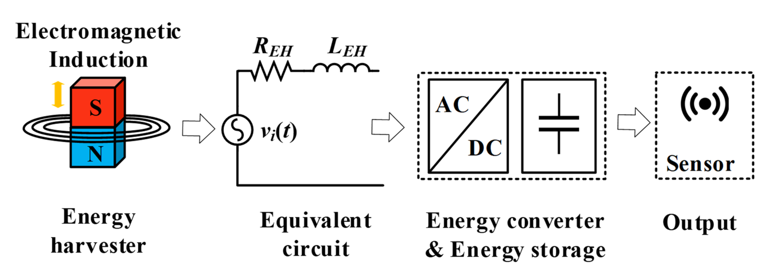
Figure 1 depicts the basic architecture of EVEH, which is composed of an energy harvester, an energy converter and an energy storage module. The energy harvester can be modeled as a voltage source
vi(
t) in series with equivalent resistance
REH and inductance
LEH. An energy converter is required to regulate the low-voltage AC to DC level.
Vibration energy in the environment has a wide dynamic range of frequencies and amplitudes. For example, the vibration of the bridge is related to its traffic flow [
7], with an average vibration frequency of around 40 Hz and a peak frequency of up to 500 Hz when two vehicles meet oppositely side-by-side [
8]. A conventional energy harvester is usually narrow banded, with one resonant frequency for maximum power harvesting [
9]. When the vibration frequency deviates from the resonant frequency of EVEH, the ability to harvest energy will decrease significantly, which lead to no or very little output power. Therefore, energy storage is necessary to provide energy to the output when the vibration fluctuates or disappears.
However, some existing works did not include a storage element [
10,
11,
12]. Existing converters with energy storages were relatively complex in circuit topology and control strategy while ensuring stable output. Although an energy storage component was included in [
13,
14], it was directly applied to power the load when vibration disappears. Such a configuration failed to maintain a stable voltage for the sensors, which leads to increased power consumptions or the degradation of the sensors’ performances [
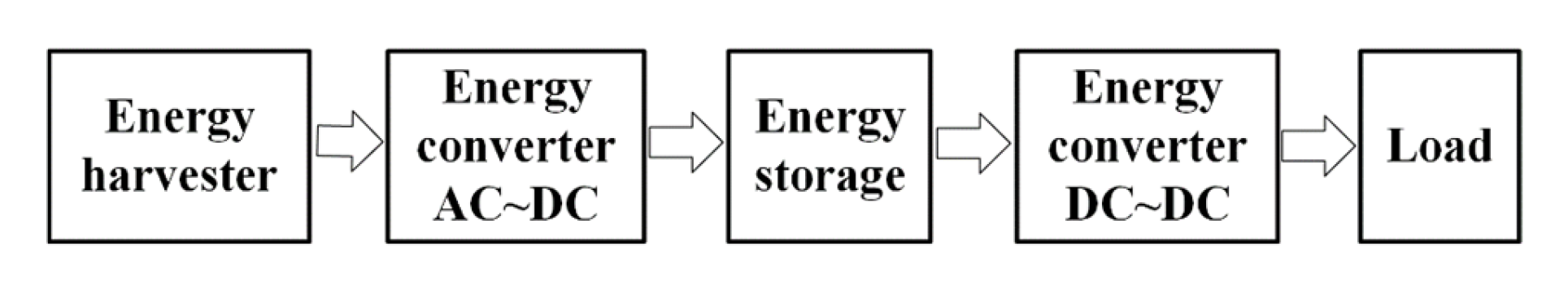
15]. In order to maintain a stable output voltage level when vibration disappears, the voltage level of energy storage component needs to be regulated before sending it to the load. As shown in
Figure 2, the energy storage module acted as an intermediate DC bus, and an additional DC-DC converter was employed to power the load [
16,
17,
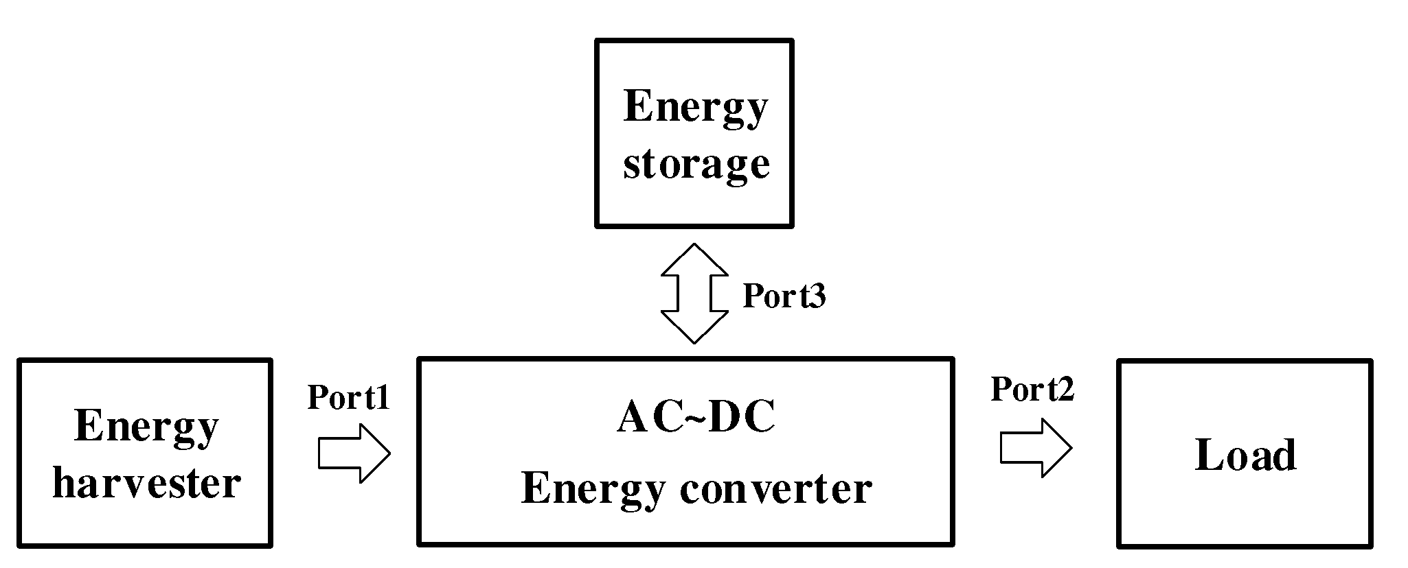
18]. Another typical approach is the three-port converter, as depicted in
Figure 3 [
19,
20]. Both the energy storage component and load are charged by the vibration source once it exists. When the vibration disappears, the energy storage component will become the power source for the load through the AC-DC converter. Such architectures and their control strategies are complex and high cost.
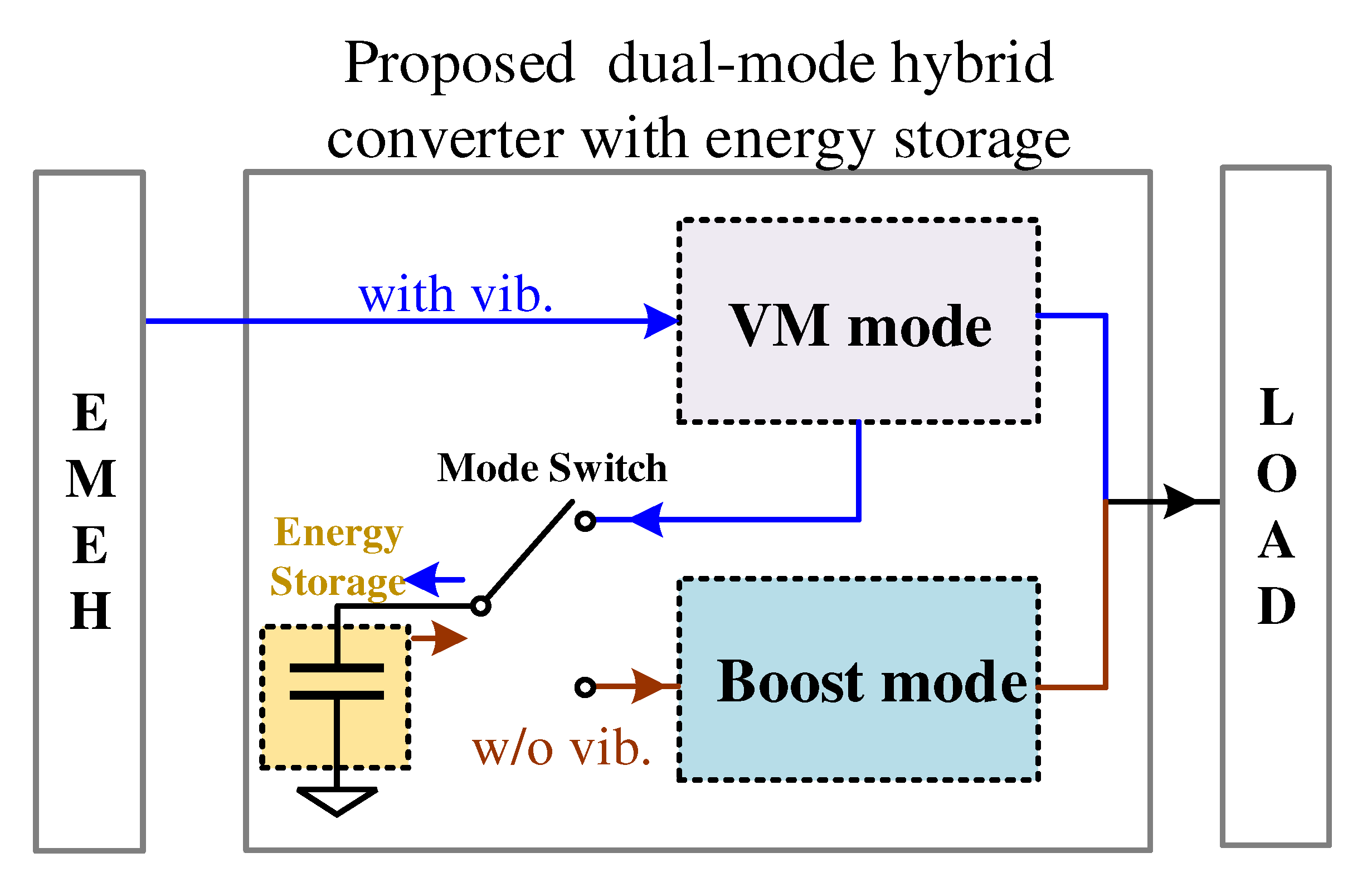
In our previous work [
21], a new dual-mode hybrid step-up converter was proposed with dual-mode operation to realize the resistance of the input vibration disturbance in a simple architecture. However, a converter based on a double-voltage circuit cannot achieve satisfactory output when the input voltage is low. In order to expand the range of input voltage, a converter based on a multiple-voltage circuit is proposed on the basis of [
21], as shown in
Figure 4. The converter merges the voltage multiplier (VM) and boost regulator, and utilizes the super-capacitor as the energy storage module. When vibration exists, the hybrid converter works in VM mode to power the load and store energy in the supercapacitor. When vibration disappears, the output is powered through the energy stored in the supercapacitor, and the hybrid converter is switched to boost mode. Furthermore, the proposed converter will start working once the output of the EVEH is higher than the forward voltage drop of the diodes and no extra start-up circuits are required [
12,
19].
The organization of the rest of the paper is as follows:
Section 2 discusses the structure and working process of the proposed converter.
Section 3 analyzes the output characteristics. Control strategies are provided briefly in
Section 4.
Section 5 explores the design principles of the proposed circuit, including the selection of the number of stages and the super-capacitor, loss analysis, targeting at sufficient voltage amplification at VM mode, and long operation duration in boost mode. The measurement results are further given in
Section 6. Finally, conclusions are drawn in
Section 7.
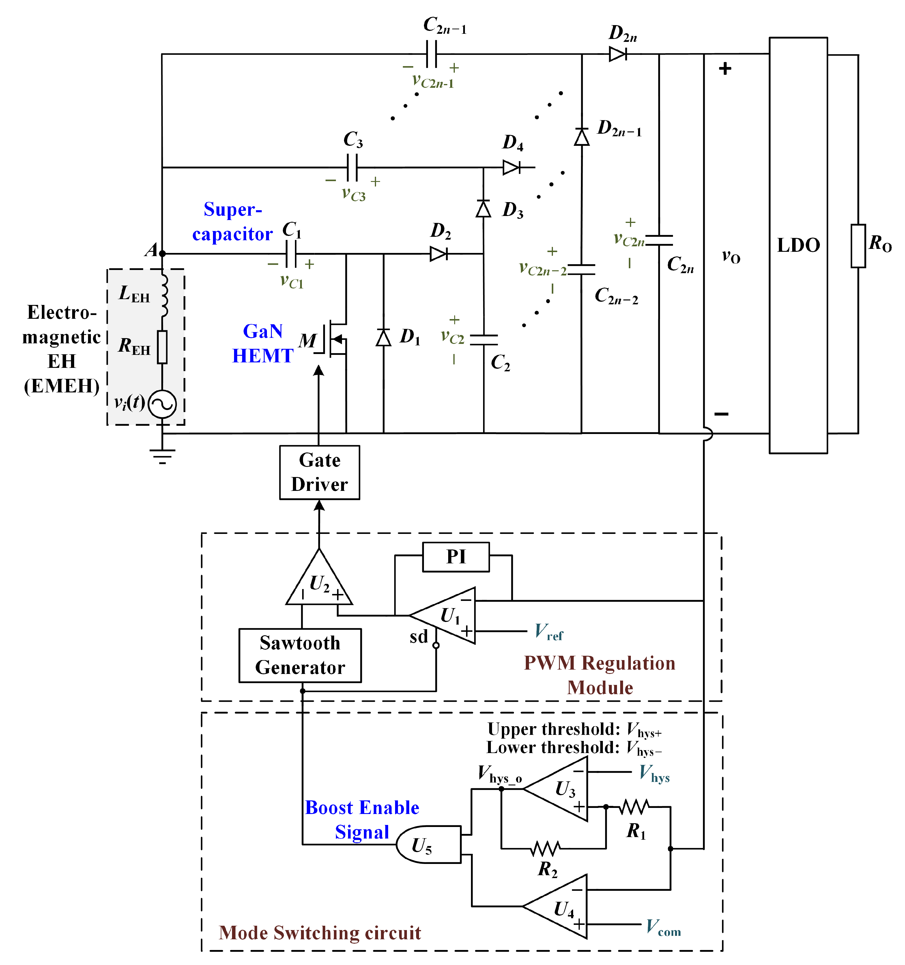
2. System Architecture and Mode Control
Figure 5 shows the full schematic of the proposed dual-mode hybrid VM-boost converter, which consists of the main power stage, the mode switching circuit and the PWM regulation module. A low-dropout regulator (LDO) is used to further stabilize the output level. The main power stage is a
n-stages VM with boost mode merged with the first stage of VM, where the winding inductance from the electromagnetic energy harvester is adopted as the boost inductor.
C1 is a large super-capacitor for energy storage and serves as an energy source when vibration disappears. The mode switching circuit determines the VM and boost operation modes for the proposed converter.
The reference voltages used in the circuit follow the relationship
VO_VM >
Vhys+ >
Vcom >
VO_boost =
Vref >
Vhys−.
VO_VM and
VO_boost represent the output for VM mode and boost mode, respectively. Under VM mode,
U1 is shut down by setting the
sd terminal at a low level. When the output falls below
Vcom because of the disappearance of vibration, the converter will switch to boost mode with the
sd terminal enabled. The output voltage is controlled by the PWM regulation module with
Vref in boost mode.
Vhys+ is used to ensure that
C1 is pre-charged first by VM mode. Otherwise, boost mode will be enabled at the system’s start-up transient. As soon as the voltage level in
C1 is dropped below
Vhys−, the converter will stop boost mode operation, and the system is shut down where there is insufficient energy in
C1 to meet the load requirement. The mode control strategies and key operation waveforms of the proposed converter are summarized in
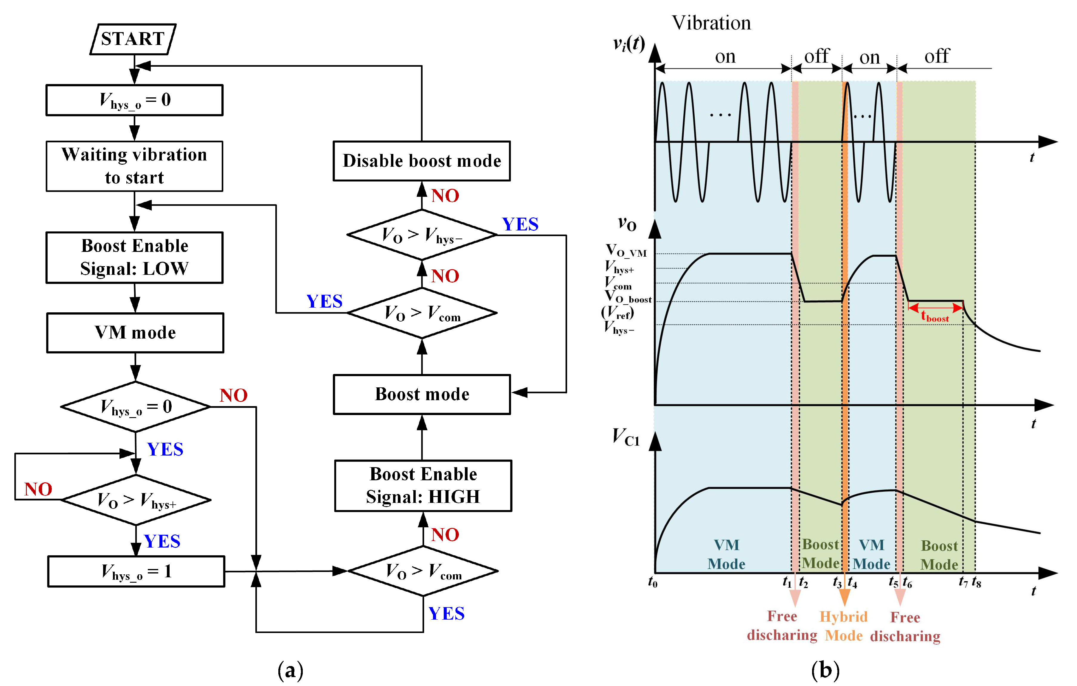
Figure 6.
t0–t1: At t0, the vibration appears and the converter starts to work in VM mode. vO will gradually rise to the stabilized value of VO_VM.
t1–t2: The vibration disappears at t1. VM mode stops and vO begins to drop according to the load requirement.
t2–t3: vO drops to Vcom at t2 and the hybrid converter will switch to boost mode. The load will be powered by C1. The output is regulated to VO_boost and the voltage of the C1 drops gradually.
t3–t4: Vibration resumes at t3, and vO begins to rise above VO_boost. However, vO is still lower than Vcom in this period, such that the boost mode is not disabled. The hybrid converter operates with the coexistence of VM mode and boost mode.
t4–t5:vO rises above Vcom at t4 and the converter starts to work in VM mode. vO will be maintained at VO_VM.
t5–t6: Vibration disappears at t5. This interval is the same as [t1–t2].
t6–t7: vO drops to Vcom at t6 and the hybrid converter will switch to boost mode. This interval is the same as [t2–t3]. The time duration for which the converter is able to provide a stable output is defined as tboost.
t7–t8: At t7, the energy stored in C1 is not enough to maintain the output at VO_boost. Although the converter is still in boost mode, vO will decrease from VO_boost.
t8–: When vO drops to Vhys− at t8, the system is shut down. The output voltage and the voltage across C1 will gradually drop to zero. If the vibration resumes, the process starting from t0 is repeated.
3. Output Characteristics
As shown in
Figure 5, the converter works in the VM mode and the main power transistor
M is off when vibration exists. When
vi(
t) is negative,
vi(
t) and
C2i(i = 1,2…n−1) charge the capacitor
C2i+1(i = 1,2…n−1) through
D2i+1(i = 1,2…n−1). According to Kirchhoff’s voltage law (KVL) and the law of the conservation of electric charge (CEC), the capacitors’ voltage in this interval can be expressed as
where
RO is the load of the converter, and
fvib is the frequency of vibration.
Vp is the peak amplitude of
vi(
t), and
VD is the forward voltage drop of the diodes. Δ
QVM is the transferred charge in one vibration period, and satisfies Δ
QVM =
VO_VM/(
RO fvib).
IVM_avg is the average current of
vi(
t).
When
vi(
t) is positive,
vi(
t) and the capacitor
C2i−1(i = 1,2…n) provide energy to
C2i(i = 1,2…n) through
D2i(i = 1,2…n). According to KVL and CEC, the capacitors’ voltage in this interval can be expressed as
By combining (1) and (2), the output of VM mode can be derived by charge conservation as
where
. According to CEC,
IVM_avg = 2
nIO = 2
nVO_VM/
RL. According to (1), the voltage over super-capacitor
C1 is charged to:
When vibration disappears, the converter will switch to boost mode and the energy stored in
C1 starts to discharge in order to provide power to the output.
Figure 7 shows the equivalent circuits and charge flow paths when
M is off and on in one switching cycle. A constant current source (
IO) is used as the load. Δ
QBoost represents the transferred charge in one switching period, and satisfies Δ
QBoost =
IO/
fs, where
fs is the switching frequency in boost mode.
When
M turns off in the (1 −
D)
Ts interval, as shown in
Figure 7a,
C1 and
LEH charge
C2 through
D2 with Δ
QBoost transferred, where
D is the duty ratio of boost mode. Simultaneously,
C3 and
LEH charge
C4 through
D4 with Δ
QBoost transferred, as do
C2i−1(i = 1,2…n) and
LEH. Therefore, the total charge dissipated from
LEH becomes
nΔ
QBoost. Assuming that the inductor current is continuous, the average inductor current can be expressed as:
IL_avg =
nΔ
QBoostfs/(1 −
D). As such, the voltage drop across
REH is
VREH =
IL_avg ×
REH = nIOREH/(1 −
D). Furthermore, the voltage of the
LEH can be derived using volt-second balance. According to KVL and CEC, the capacitors’ voltage in this interval can be expressed as
where
is the voltage across
LEH and
REH when
M is off.
As shown in
Figure 7a, when
M is on in the
DTs interval,
C1 charges
LEH with Δ
QLEH. Simultaneously,
C1 and
C2 charge
C3 through
D3 with Δ
QBoost, and
C1 and
C4 charge
C5 through
D5 with Δ
QBoost, as do
C1 and
C2i−2(i = 2,3…n). Hence, Δ
QLEH equals to
nΔ
QBoostD/(1 −
D). According to KVL and CEC, the capacitors’ voltage in this interval can be expressed as
where
is the voltage across
LEH and
REH when
M is on.
Assuming that the voltage across
C1 does not change in one switching period—e.g.,
—
VO_boost can be expressed according to (5)–(8):
where
.
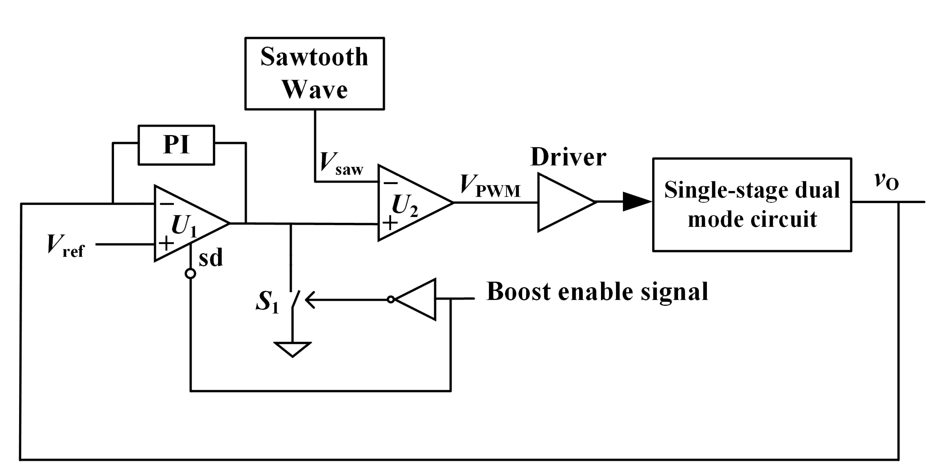
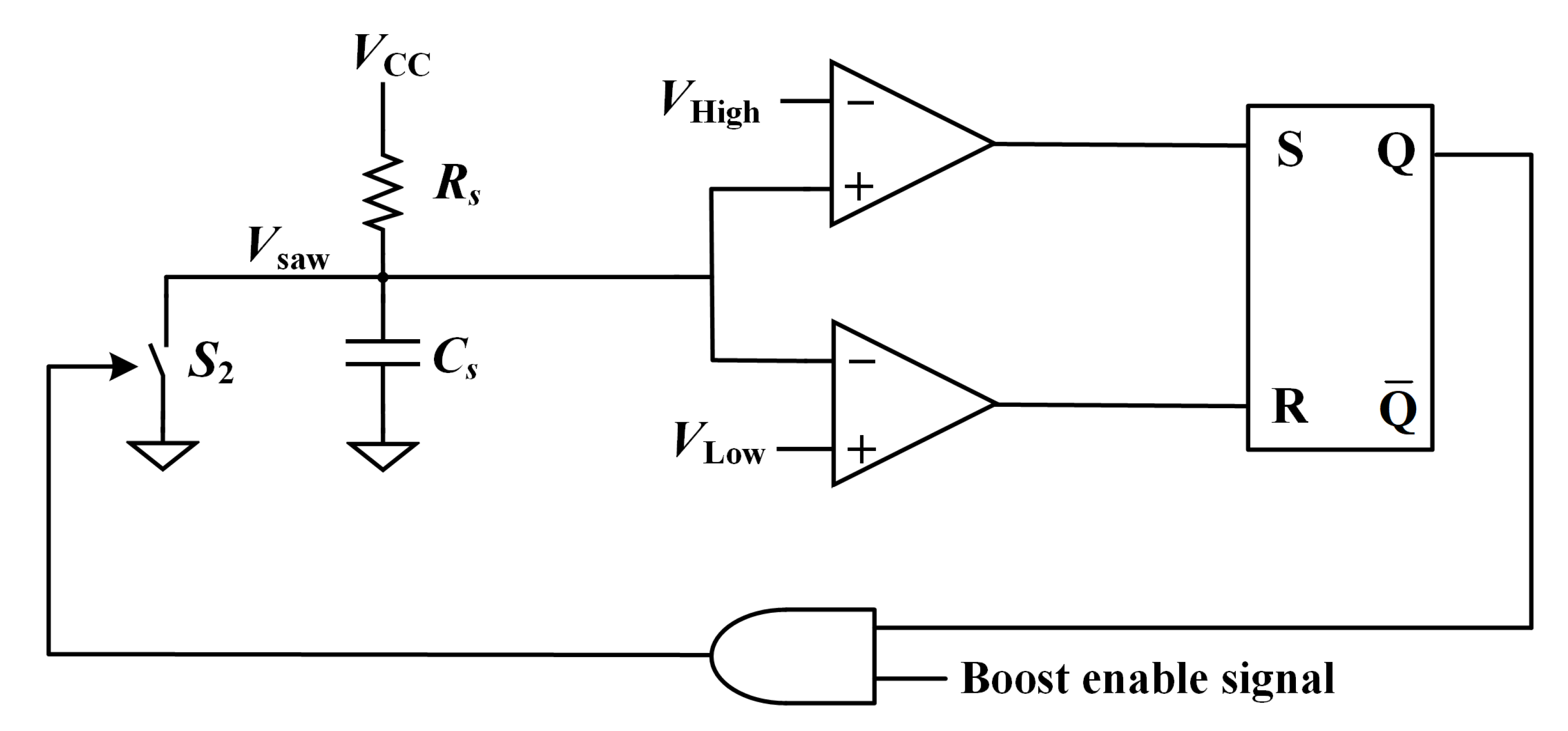
4. PWM Regulation for Boost Mode
A PI-based PWM regulation is adopted for output control under boost mode, as shown in
Figure 8 and
Figure 9. The PI output is compared with the sawtooth wave (
Vsaw) to generate the PWM signal for the gate driver of GaN HEMT devices (
M). The sawtooth generator is composed of series resistor
Rs, capacitor
Cs, two voltage comparators, a RS trigger, and switch
S2, as shown in
Figure 9. The two voltage thresholds are set as
VHigh and
VLow (
VHigh >
VLow). If
Vsaw is higher than
VHigh or lower than
VLow, the status of the RS trigger changes to control the on and off of
S2. According to the RC charging theorem, the frequency of the sawtooth wave can be expressed as
To avoid the mode oscillations during mode switch,
S1 is closed in order to maintain the output of the PI regulator at a low level under VM mode, as shown in
Figure 8.
5. Key Parameters and Analysis
As can be seen from (3) and (9), the output voltage of the proposed hybrid converter is dependent on the number of stages and the design of the super-capacitor. In order to realize sufficient voltage amplification at VM mode and ensure a long operation duration (tboost) in boost mode, these two parameters are fully studied in this section. In the meantime, the loss distributions of VM mode are analyzed, which also leads to the optimum design of the number of VM stages.
5.1. Selection of the Number of Stages
For VM mode, the VM converter needs to tolerate the variations of the load resistors (
RO) and
REH. Assuming that
C1 =
C2 = … =
C2n =
C, the minimum required number of stages can be derived through (3), as
where
.
VO_VM increases first, then decreases with the increase of the number of stages.
nmax is defined as the number of stages when the output voltage reaches its maximum value under a certain input. The
nmax for the peak output voltage at a certain load resistor can be deduced from
, as
Hence, with an LDO post-regulation, the possible number of stages for a certain
VO_VM should be chosen as
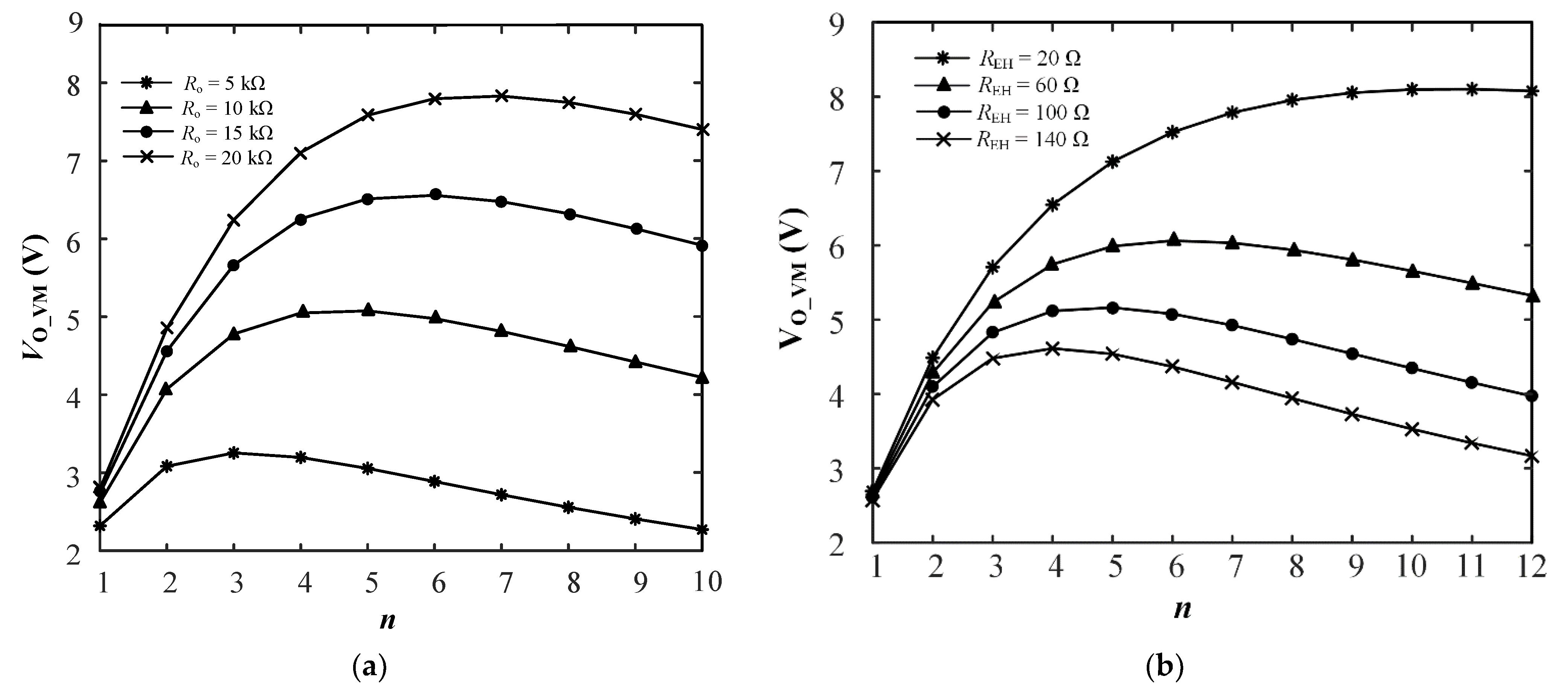
Figure 10a describes the relationship between the number of stages and
VO_VM with different
RO at an
REH of 100 Ω. The higher
RO is, the smaller the number of stages required for a certain
VO_VM.
Figure 10b describes the relationship between the number of stages and
VO_VM with different
REH at
RO of 10 kΩ. The higher
REH is, the larger the number of stages required for a certain
VO_VM. According to (1), the minimum
RO for a certain output
VO_VM can be derived as
If RO ≤ RO(min), the converter can’t stabilize to VO_VM. If the load RO > RO(min), the LDO module is required to further stabilize the output to VO_VM.
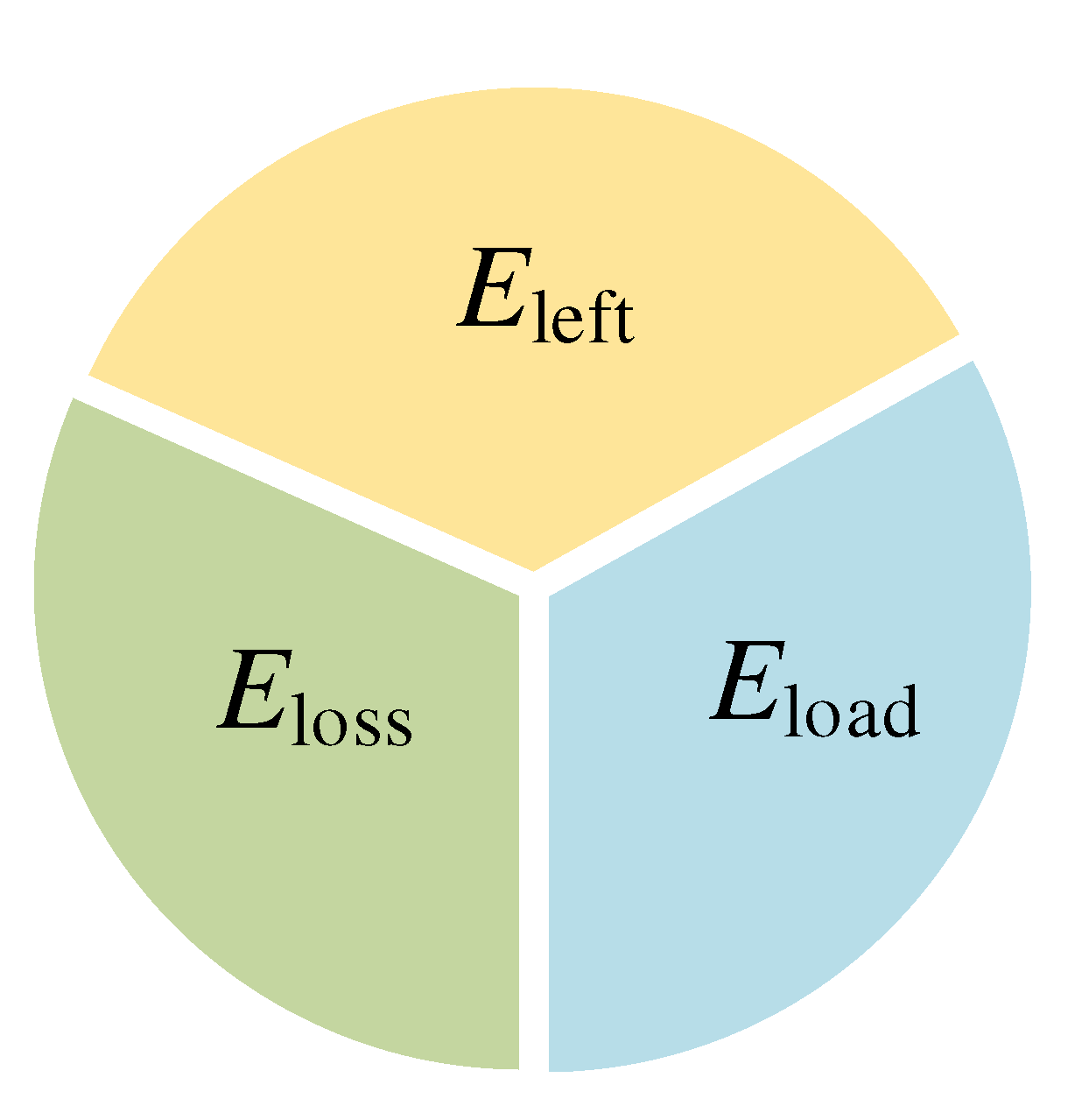
For boost mode, the main target is to provide a stable output as long as possible when vibration disappears. Considering that
C1 reaches a steady state before vibration disappears, the total energy stored in
C1 will be divided into three parts in boost mode, as shown in
Figure 11:
Eload is the energy transferred to the output;
Eloss is the energy dissipated in the circuit, and
Eleft represents the energy leftover in
C1 when the output fails to be regulated to
VO_boost. Therefore,
Etotal_C1 =
Eleft + Eload + Eloss. In order to extend the duration for a stable output when vibration disappears,
Etotal_C1 should be large and the proportion of
Eload should be as large as possible for a certain
Etotal_C1.
The initial voltage across the super-capacitor C1 in boost mode (VC1_max) can be derived by (4). The larger VC1_max is, the larger Etotal_C1 will be. VC1_max decreases with the increase of n.
When the converter operates at maximum duty cycle
Dmax,
C1 reaches to its minimum voltage level to be capable to provide a well-regulated
VO_boost.
Dmax can be obtained by forcing d
VO_boost/d
D = 0. Therefore, the minimum
VC1 to maintain
VO_boost becomes:
The lower VC1_min is, the lower Eleft will be. As VC1_min increases with the increase of n, the more number of stages adopted, the more proportion of Eleft will be.
The total transferred charge of
C1 (
QC1_output) is directly related with
Eload + Eloss in one boost period, as
It can be seen that the more number of stages will be, the more charges are required from C1 to power the output for a certain tboost under the same load and output voltage. It can be concluded that Eload is reversely proportional to the number of stages under certain Etotal_C1. Hence, combing the two aspects for both with (VM mode) and without (Boost mode) vibration, the minimum feasible number of stages (nmin) should be selected.
5.2. Design of Super-Capacitor C1
In order to ensure that the selected
C1 can provide sufficient energy during required
tboost time interval,
C1 is designed under the most extreme condition where maximum duty ratio is always applied. It is the situation when the discharge rate of
C1 is highest. According to (16),
C1 can be chosen as
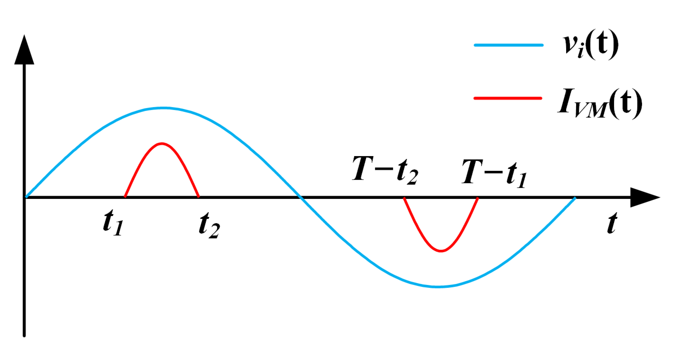
5.3. Loss Analysis
As the VM mode is the main circuit processing EH power, the power consumptions of VM mode are discussed in this section. In EVEH,
REH is usually much larger than the impedance of winding inductance of
jωLEH, so that
LEH is ignored the loss analysis. The charging current of capacitor is shown in
Figure 12, where
IVM(
t) is the current of EH source. Capacitors are only charged during the intervals of
t1~
t2 and (
T −
t2~
T −
t1) in one vibration period.
In negative half period, odd number capacitors
C2i−1(i =1, 2…n) in
Figure 5 are charged by EH source with the following relationships satisfied:
In positive half period, even number capacitors
C2i(i =1, 2…n) in
Figure 5 are charged with the following formula satisfied:
Ignoring the voltage variations in
C1 as it is quite large,
IVM(
t) can be calculated as
where
and
.
5.3.1. Loss of REH
REH is the output resistance of the EVEH source and its power loss can be expressed as
5.3.2. Loss of Capacitors’ Charge Transfer
When the charge
is transferred from capacitor
A (
CA) with initial voltage
uA to capacitor
B (
CB) with initial voltage
uB, according to CEC, the loss of charge transfer is:
In each vibration period, Δ
QVM is transferred between the
Ci(i = 1,2…2n) and
Ci+1(i = 1,2…2n−1). Assuming that
Ci(i = 2…2n) is large enough with ignorable voltage ripples, the loss of
Ci(i = 1,2…2n) in the process of charge transfer can be expressed as
5.3.3. Loss of Diodes
Diode
Di(i = 1,3…2n − 1) and
Di(i = 2,4…2n) turns on during time intervals (
t1~
t2) and (
T −
t2~
T − t1) respectively in each EM period. Hence, diodes’ conduction losses can be described as
When diodes are off, leakage current will also induce loss, as
where
Ileak is the reverse leakage current of diodes. Therefore, the overall losses of diodes can be expressed as
5.3.4. Loss of Super-Capacitor
Super-capacitors have large series resistors in the order to tens of ohms. The power consumptions on the parasitic resistor (
RC1) can be expressed as
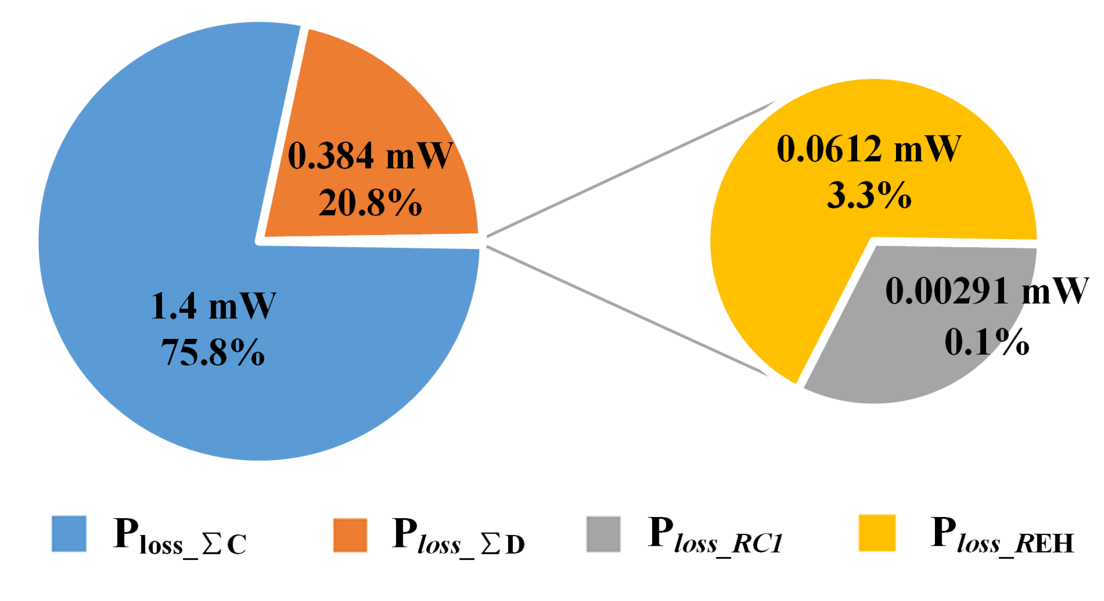
In order to evaluate the loss contributions in the VM mode of the proposed circuit, the circuit parameters are given in
Table 1. As shown in
Figure 13, the charge transfer loss is the major loss contributor, which is 75.8% of the total losses. The second largest loss contributor is diode conduction loss, which accounts for 20.8% of the total losses. Both the charge transfer loss and diode conductor loss increase with the increase of the number of stages (
n). The power losses on EVEH’s internal resistor and parasitic resistor at the super capacitor are negligible. Therefore, the minimum number of stages to provide sufficient output voltage level should be used. This conclusion is also consistent with the discussions in
Section 5.1.
6. Prototype Design and Measurement Results
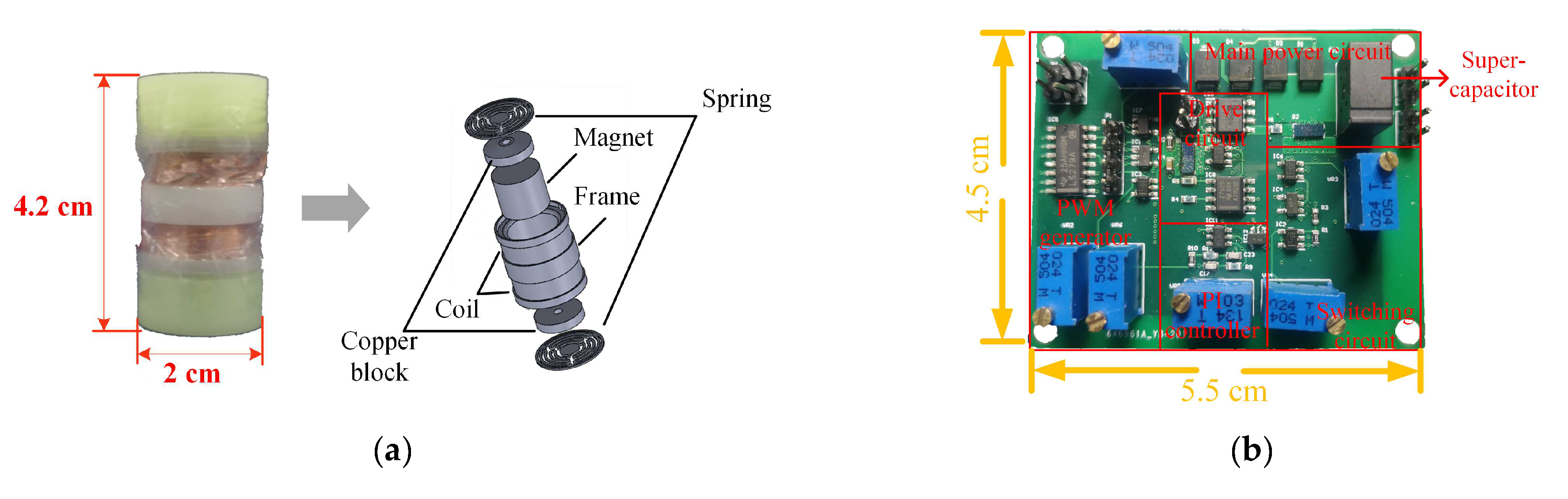
A cylindrical EVEH [
22] is employed in this experiment as the source for the proposed dual-mode converter. As shown in
Figure 14a, it is designed with a cylindrical magnet, two planar springs connected to the top and bottom of the magnet, and two sets of windings. The measured winding resistance
REH and inductance
LEH are 105 Ω and 5.1 mH, respectively. The designed EVEH has a 4.2-cm height and a 2-cm diameter. At a vibration resonance frequency of 100 Hz and an acceleration of 0.7 g, the AC output amplitude (
Vp) reaches 1.8 V. The prototype of the dual-mode hybrid step-up circuit is shown in
Figure 14b. A Schokky diode (VS-10BQ015HM3) with a low forward conduction voltage of 0.3 V is used. A GaN HEMT EPC2015C (40 V/53 A) is employed as the main switching transistor.
Vcom,
Vhys,
Vhys+ and
Vhys− are set to 3.4 V, 2.25 V, 3.6 V and 0.6 V, respectively.
Vref for the boost mode output is set to 3.3 V. According to (11), the number of stages should be chosen as two. The key parameters used in this design are summarized in
Table 2.
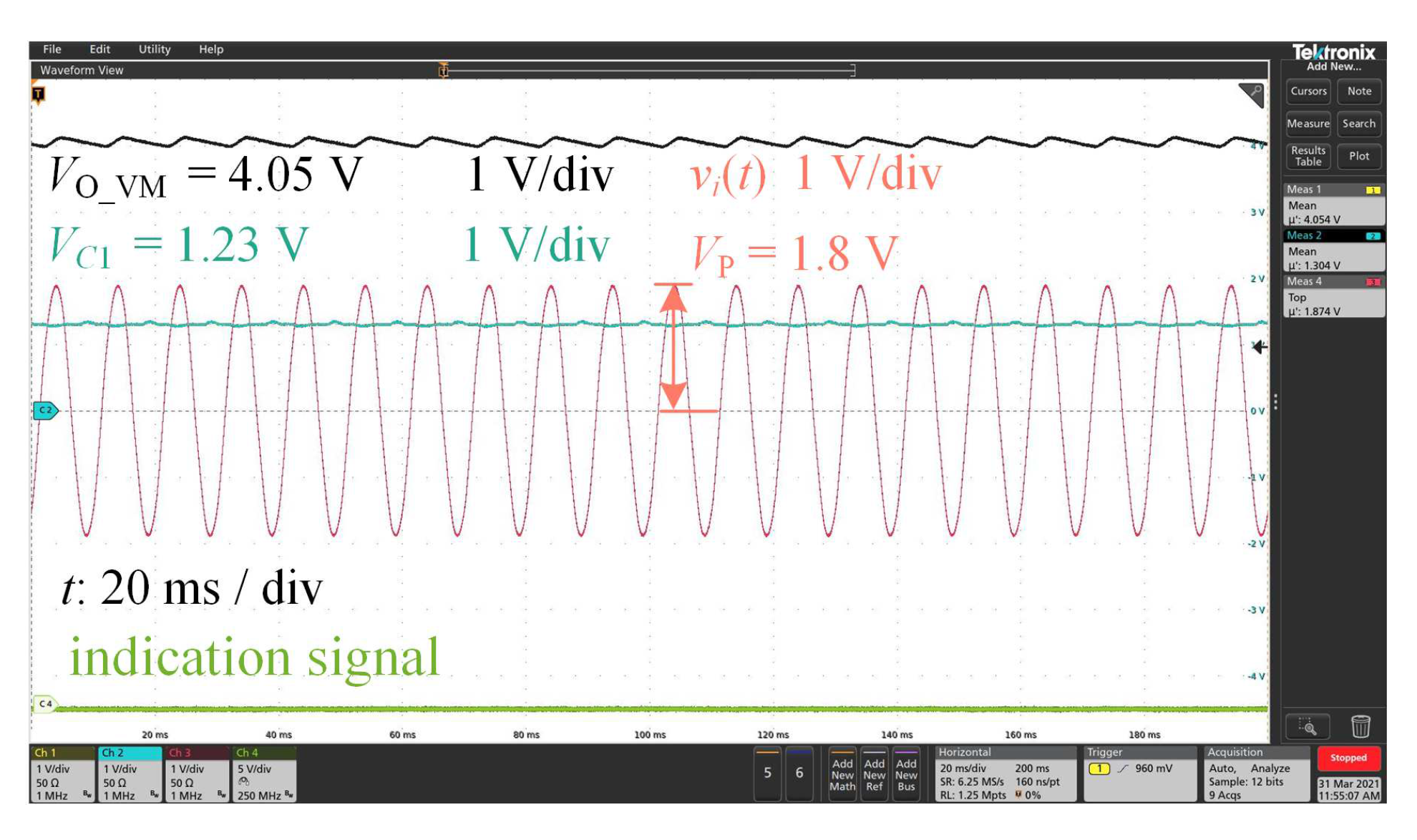
Figure 15 shows the waveforms of VM mode operation under vibration. The output voltage of the VM circuit and voltage across the supercapacitor are maintained at 4.05 V and 1.23 V, respectively.
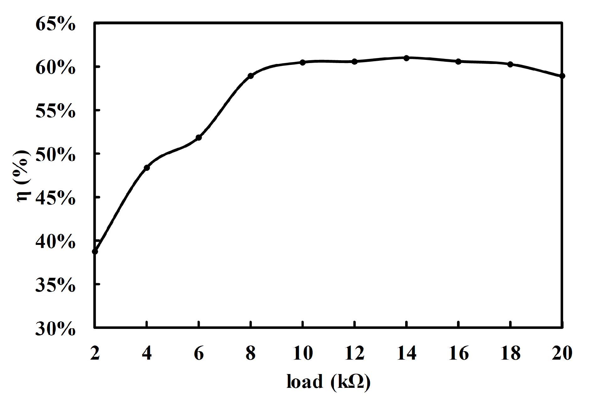
Figure 16 shows the circuit efficiency (
η) of the VM circuit when
n = 2 with different load resistors and the same
Vp, where the peak efficiency reaches 60.7%.
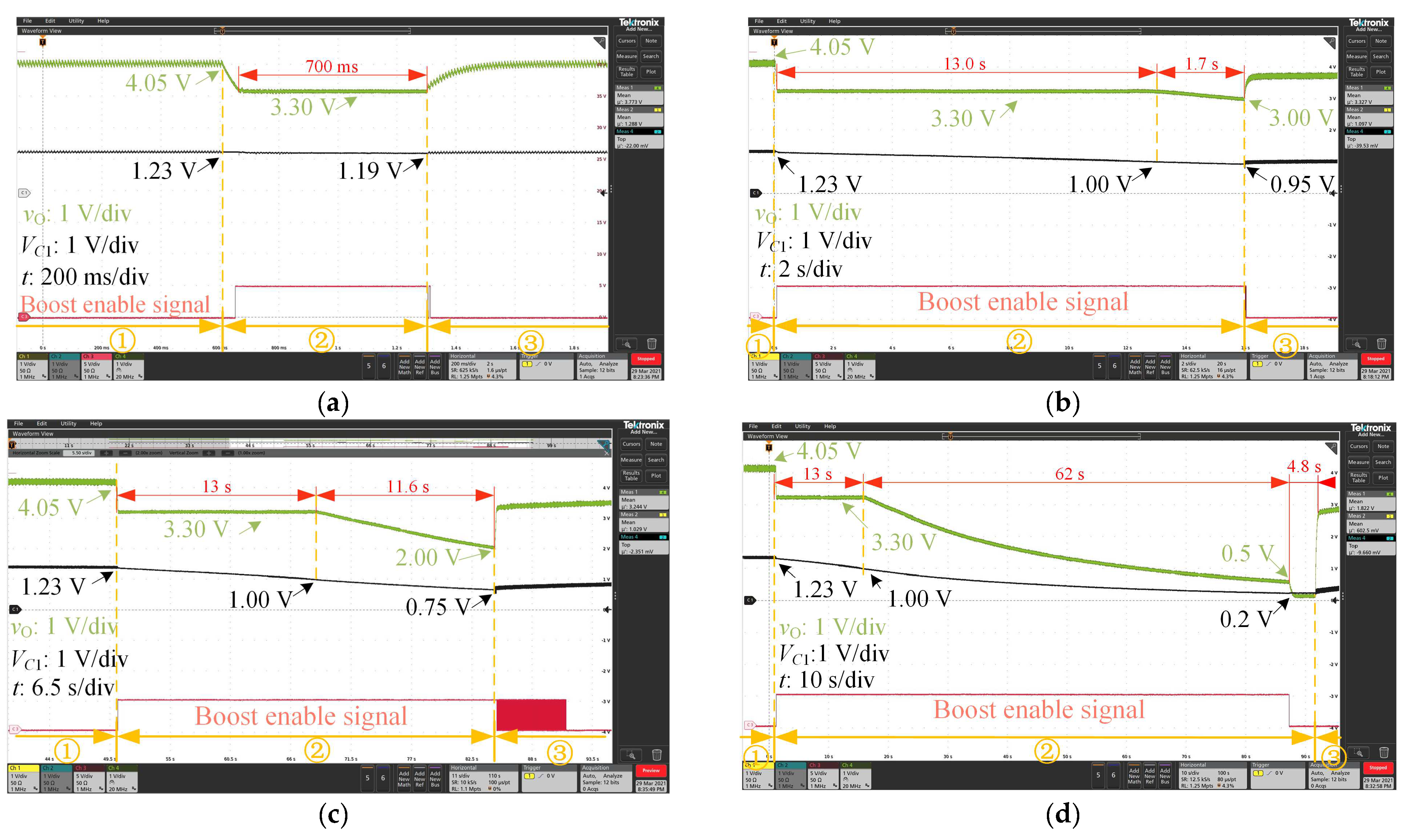
Figure 17 reveals the different cases of the operation modes transitions from the existence (①) of vibration to the disappearance of vibration (②) and the resumption of vibration (③). Four different cases are studied:
Case 1: In
Figure 17a, the vibration is resumed after 700 ms of disappearance.
vO is stabilized to 3.3 V during the disappearance period.
VC1 drops to 1.19 V from 1.23 V.
vO and
VC1 rise to 3.3 V and 1.23 V after vibration is resumed, respectively.
Case 2: In
Figure 17b, the vibration is resumed after a 14.7-s disappearance.
vO is stabilized to
VO_boost (3.3 V), and
VC1 drops to 1.0 V from 1.23 V in the first 13 s. After 13 s, the boost mode cannot keep
vO to
VO_boost, and
vO begins to decrease. At 14.7 s,
vO drops to 3 V and
VC1 drops to 0.95 V.
vO and
VC1 rise to 3.3 V and 1.23 V after vibration is resumed, respectively.
Case 3: As shown in
Figure 17c,
vO is stabilized to 3.3 V for 13 s and drops after the vibration’s disappearance. The vibration is resumed after a 24.6-s disappearance, and the output rises again. However, the boost mode-enabled signal switches between high and low within a short time, starting from the time that
vO rises near to
Vcom. This is caused by the output voltage fluctuating around
Vcom in the process of rising.
Case 4: As shown in
Figure 17d, after the first 13 s of well regulation,
vO begins to drop. At 75 s,
vO drops to 0.5 V, which is lower than
Vhys−, and the boost mode is shutdown. The vibration is resumed after 79.8 s disappearance, and the converter is restarted.
As depicted in
Figure 17b–d, the time of voltage stabilization of the circuit is 13 s, which is 30% lower than the calculation results. This is because the large ESR (50 Ohms) of the selected super-capacitor consumes lots of stored energy in
C1.
Figure 18 shows the operation mode switches with the changes of external vibration. When the vibration disappears (e.g., region ②④⑥⑧), the boost-enabled signal becomes high. The circuit works under boost mode and the supercapacitor starts to discharge.
vO is stabilized at
VO_boost (3.3 V). When external vibration resumes (e.g., region ①③⑤⑦⑨), the output
vO starts to increase above
Vcom and the boost-enabled signal becomes low. The circuit switches back to VM mode and the supercapacitor voltage starts to rise. This shows that the circuit has a strong capability to maintain a stable output when the vibration is unstable. With an extra LDO stage, the output voltage can be better regulated.
Table 3 summarizes the performance of the proposed dual-mode hybrid step-up converter and compares it with state-of-art power converters in EVEH applications. Compared with active VM circuits [
23,
24] and direct AC~DC dual boost converters [
12,
14,
25,
26] where energy storages were not included, the proposed work has the advantage of continuously providing energy when the vibration disappears in a simple hybrid topology. In the meantime, it can achieve almost the same efficiency as a dual boost circuit with a much simpler control method. Some studies [
16,
18,
27] adopted energy storage as the intermediate stage, as shown in
Figure 2. The efficiencies of the topology given in [
16,
18] were lower than the proposed circuit due to the two-level transformation. One study [
27] reported a high conversion efficiency of 85% and a stable output when the vibration source disappeared, but only simulation results were presented, and the output power was tens of orders lower than the proposed work. One study [
19] described a three-port converter with additional battery as the energy storage. A microcontroller was employed for MPPT control, which is quite power consuming and is not suitable for milli-power applications. The total efficiency was not reported in [
19]. Furthermore, the state-of-arts in
Table 3 all require extra start-up circuits, which may induce high energy loss with discrete components. Hence, the proposed dual-mode hybrid converter has been demonstrated to achieve a decent efficiency for EH energy conversion, and provides continuous output under unstable vibrations in a simple system architecture.
7. Conclusions
A dual-mode hybrid step-up circuit with stable output for vibration energy harvesting (EH) was proposed in this paper. The converter operates as a multi-stage voltage multiplier when vibration exists, with the supercapacitor and output load both powered. Once vibration disappears, it will switch to boost mode, and the supercapacitor is employed as a power supply. The selections of the number of stages and supercapacitor are based on the voltage gain characteristics under different input and output impedance and the system’s energy utilization. A GaN HEMT-based dual-mode prototype was designed and tested with an in-house-designed EVEH device. Different operation modes were fully verified. When n = 2, the output voltage of the prototype reaches 4.05 V/1.64 mW in the existence of a vibration of 0.7 g and 100 Hz. The proposed converter is able to stabilize to 3.3 V in the absence of vibration for 13 s. The peak output efficiency of a hybrid circuit reaches 60.7%. The proposed hybrid converter has been demonstrated to achieve a descent efficiency for EH energy conversion, and provides continuous output under unstable vibrations in a simple system architecture without the need for an extra start-up circuit. It is a premium solution for a low-voltage, low-power EVEH system with unstable vibrations.
Future work will focus on the following two aspects. One is the low-voltage integration of the converter to reduce the loss brought about by discrete devices and parasitic interconnection. For example, the discrete Schottky diodes adopted in this paper suffer from high forward conduction because diodes with a voltage rating of 15 V and a current rating of 1 A are employed, which are far beyond the actual voltage and current requirements in the proposed application. Voltage/current-suitable devices will be available through IC integration, which will further improve the overall efficiency. The other focus is to apply the design of the energy harvester and hybrid step-up converter considering the specific vibration environment and load characteristics.


