Article

Development of a Thermal Energy Harvesting Converter with Multiple Inputs and an Isolated Output

1
Department of Ph.D. Program, Prospective Technology of Electrical Engineering and Computer Science, National Chin-Yi University of Technology, No. 57, Sec. 2, Zhongshan Rd., Taiping Dist., Taichung 41170, Taiwan
2
Department of Electrical Engineering, College of Electrical Engineering & Computer Science, National Taipei University of Technology, 1, Sec. 3, Zhongxiao E. Rd., Taipei 10608, Taiwan
3
Department of Electrical Engineering, College of Information & Electrical Engineering, Feng Chia University, No. 100, Wenhwa Road, Seatwen, Taichung 40724, Taiwan
*
Author to whom correspondence should be addressed.
Energies 2022, 15(1), 273; https://doi.org/10.3390/en15010273
Submission received: 26 November 2021 / Revised: 13 December 2021 / Accepted: 20 December 2021 / Published: 31 December 2021
(This article belongs to the Topic Thermoelectric Energy Harvesting)

Abstract

:
In this paper, an isolated multi-input single-output (MISO) converter is developed and applied to a thermoelectric energy conversion system to harvest thermal energy. The thermoelectric generators have individual maximum power point tracking functions. Furthermore, such a converter has a high step-up voltage conversion ratio. In addition, the presented converter is imposed on the thermoelectric energy conversion system with the three-point weighting strategy adopted to realize the maximum power point tracking (MPPT). In this paper, the basic principles of this converter are first described and analyzed, and finally some simulated and experimental results are offered to verify the feasibility and effectiveness of such a thermal energy harvesting system.

1. Introduction

As generally recognized, from the point of view of industrial applications, 50% of generated electricity is used, while the remainder is wasted via heat. Accordingly, if the heat can be changed to electricity, then the energy conversion efficiency can be increased, and the pollution due to exhaust heat and emissions due to exhaust gas can be decreased [1]. At present, many methods have been proposed to recycle exhaust heat into electricity—for example, the organic Rankine cycle, combination of power and heat, thermoelectric generators (TEGs), etc.; of these, TEGs have many features, such as small size, no noise, easy maintenance, easy extension, etc. In fact, the process of recycling thermal energy is quite similar to that of recycling solar energy—both of which require the maximum power point tracking (MPPT) to harvest thermal energy efficiently.
Therefore, there are several configurations for converting heat to electricity using a TEG. TEG-based electrical systems can be divided into three types: single TEGs [2,3], distributed TEGs [2,3,4], and centralized TEGs [2]. The first type adopts a single heat source, while the other two types use multiple heat sources. However, the first type has a limited power level, the second type is limited in terms of size and cost, and the third faces the problem of the failure of one TEG.
Therefore, a multiple-input TEG system is proposed to conquer these disadvantages. To construct a single-stage thermoelectric energy conversion system with multiple TEG inputs, a high step-up converter is indispensable. The authors of [5,6,7,8,9,10,11,12,13,14] propose several kinds of multi-input single-output converters (MISOCs) with non-isolation. The authors of [6] utilized a switched-capacitor circuit so that a high voltage gain could be achieved. The authors of [5,11,14] adopted elementary circuit configurations, leading to the corresponding voltage gains not being high. The authors of [11] employed an elementary circuit configuration together with an auxiliary circuit, such that the zero-voltage switching (ZVS) could be achieved but the accompanying voltage gain was not high. The authors of [6,9,10] utilized coupled inductors so that the voltage gains could be improved and the ZVS could be realized. However, if the number of input voltages is increased, then the number of coupled inductors and switches is increased, resulting in the huge size needed. The circuit concept displayed in [12] is derived from [14], and this converter adopts only a single inductor to obtain a result identical to that of [14], thus decreasing the size significantly; however, this converter employs an elementary circuit configuration, resulting in the voltage gain not being high; moreover, the control of such a converter is relatively complicated. The authors of [13,15] achieved high step-up voltage gains by utilizing bootstrap circuits; however, these circuits have automatic current balance, making them unsuitable for MPPT use. Consequently, the authors of [16] presented interleaved switches for the circuit shown in [15] to conquer this problem, so that each thermoelectric generator would have its own MPPT function.
For galvanic isolation to be considered, the authors of [17,18] proposed an isolated MISO high-step-up converter; however—considering that the higher the turns ratio, the greater the leakage inductance and the larger the primary-side current—the actual voltage conversion ratio remains not particularly high. In [19], the multiple inputs had individual resonant networks and coupled inductors, causing switches to have ZVS turn-on, the number of components to be relatively large, and the corresponding maximum voltage gain to be less than 1.5. In [20], a single coupled inductor was used to harvest energy from multiple heat sources; however, the duty cycle for each input has its own limitations, and the overall voltage gain is determined only by the turns ratio.
In fact, none of the converters described previously—except for the converter displayed in [16]—are used in thermoelectric systems. Accordingly, an isolated MISOC circuit is proposed herein and imposed on a thermoelectric energy conversion system.

2. Features of the Thermoelectric Module

The operation of the thermoelectric module is based on the Seebeck effect; this means that the movement of major P-type and N-type carriers due to temperature differences between the hot side and the cold side forms a current. In Figure 1a, the model of the thermoelectric module is represented by one open-circuit voltage Voc and one internal resistance Rteg. In this figure, the voltage across the variable load resistance RL is Vteg, and the current flowing into RL is Iteg. In Figure 1b, if RL is infinite, then Vteg is equal to Voc; if RL is zero, then Iteg is equal to Isc (In Figure 1c), which is Voc divided by Rteg. Therefore, based on the maximum power transfer theory under the condition that RL = Rteg [21,22], we can find the maximum power point (MPP) at:
V t e g = 0.5 V o c   and   I t e g = 0.5 I s c
Hence, the maximum power—represented as Pmpp—is identical to:
P m p p = 0.25 V o c I s c
Accordingly, the P–I–V curves of TEG are drawn in Figure 2. From this figure, it can be seen that these curves are of high symmetricity.

3. Three-Point Weighting Strategy for MPPT

Based on Figure 1, the three-point weighting strategy was adopted to derive the maximum power transfer from the TEG to the output. Figure 3 displays the operating procedure of this method, and the corresponding operation is shown in Figure 4 with three cases: for case 1, Pa > Pb > Pc; for case 2, Pa < Pb < Pc; for case 3, Pb > Pa and Pc. As in case 3, the point of the maximum power can be obtained. Note that Dmpp, Da, Db, and Dc are defined to be the duty cycles at the maximum power point, point a, point b, and point c, respectively.

4. Proposed Isolated MISOC

Figure 5 shows the proposed two-input single-output isolated high-step-up converter, which is composed of one input inductor L, one output inductor Lo, one coupled inductor constructed by one inductance, one leakage inductance with the primary winding Np, the secondary winding Ns, a turns ratio of ( n = Np/Ns), two main switches S1 and S2, three charge pump capacitors C1, C2, and C3, three diodes D1, D2, and D3, and one output capacitor Co. As for the output load, it consists of one output resistor Ro.
Before dealing with this section, we must first define some symbols shown in Figure 5 and several constraints, as follows: (1) the two input voltages are signified by Vin1 and Vin2; (2) the two input currents are indicated by iin1 and iin2; (3) the output current is expressed by Io; (4) the output voltage is denoted by Vo; (5) the voltages across C1, C2, and C3 are represented by VC1, VC2, and VC3, respectively; (6) the pulse-width modulation (PWM) signals for S1 and S2 are signified by vgs1 and vgs2, respectively; (7) the voltages across L, Lm, Lo, Np, Ns, and Llk are indicated by vL, vLm, vLo, vNp, vNs, and vlk, respectively; (8) the voltages across D1, D2, and D3 are described by vD1, vD2, and vD3, respectively; (9) the currents in L, Lm, Lo, Np, and Ns are signified by iL, iLm, iLo, iNp, and iNs, respectively; (10) the currents in D1, D2, and D3 are denoted by iD1, iD2, and iD3, respectively; (11) the duty cycles of vgs1 and vgs2 are expressed by Da and Db, respectively, under the same switching period of Ts; (12) all the components are regarded as ideal, except for S1 and S2; (13) the converter works in the continuous current mode (CCM); (14) all of the waveforms are drawn in the steady state, and four states over one cycle are illustrated in Figure 6, to be analyzed as follows:

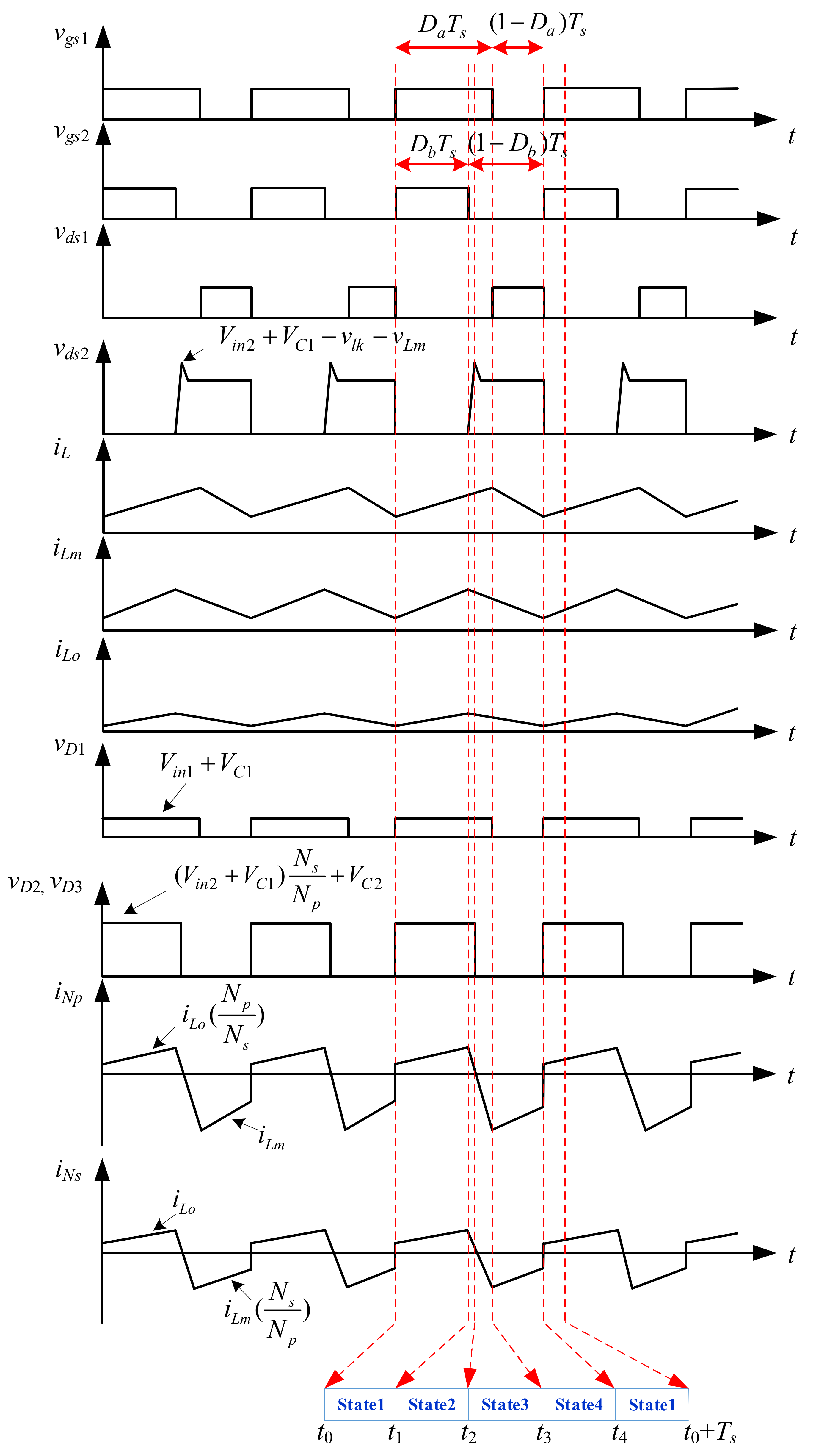
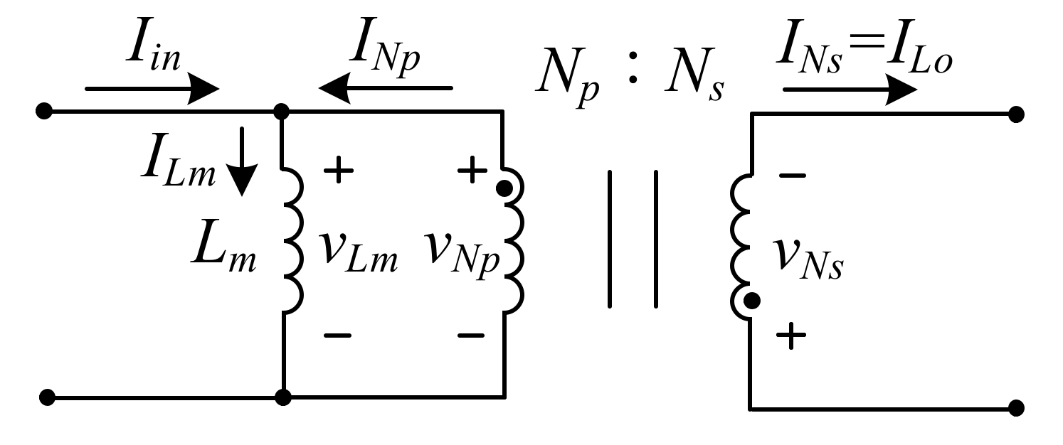
4.1. Operational Behavior

State 1 [ t o t t 1 ]: As illustrated in Figure 7, S1 and S2 are turned on, whereas D1, D2, and D3 are reverse-biased. During this time interval, L is magnetized by Vin1, whereas Lm, Llk, and Lo are magnetized by Vin2 and C1. At the same time, C2 and C3 are series-connected, and release energy to the load. In addition, D1 is reverse-biased with the voltage of Vin1 + VC1, D2 is reverse-biased with the voltage of (Vin2 + VC1)/n + VC2, and D3 is reverse-biased with the voltage of (Vin2 + VC1)/n + VC3 with VC2 = VC3.
State 2 [ t 1 t t 2 ]: As illustrated in Figure 8, S1 remains in the on-state, but S2 is turned off, whereas D1, D2, and D3 remain reverse-biased. During this time interval, L is still magnetized by Vin1, whereas Lm, Llk, and Lo are demagnetized. Since iNp remains in the positive direction, the second-side circuit operation is the same as in state 1. In addition, the leakage inductance ilk releases energy as well as charging the parasitic capacitor of S2, leading to a spike voltage on S2. The moment iN2 falls to zero, this state proceeds to the end.
State 3 [ t 2 t t 3 ]: As illustrated in Figure 9, S1 remains in the on-state, but S2 remains in the off-state, whereas D1 is turned off but D2 and D3 remain in the on-state. During this time interval, L is still magnetized by Vin1, whereas Lm and Lo are still demagnetized, and charge C2 and C3, thereby causing C2 and C3 to be paralleled with VC2 = VC3. Once the switch S1 is turned off, this state ends.
State 4 [ t 3 t t 4 ]: As illustrated in Figure 10, S1 and S2 are both off, whereas D1, D2, and D3 are all reverse-biased. During this time interval, L releases energy to C1. In the meantime, Lm is still demagnetized, so the secondary-side circuit operation is the same as in state 3. As soon as S1 and S2 are turned on, this state comes to an end, and the next period starts.

4.2. Output Voltage

To conveniently obtain the voltages on C1, C2, C3, and Co, only states 1, 3, and 4 are taken into account, and Llk is omitted. First, the turns ratio of the transformer is defined as follows:
N p N s < 1   and   n < 1
As illustrated in state 1 in Figure 7, based on Kirchhoff’s voltage law, the respective voltages across the input inductor L, the magnetizing inductance Lm, and the output inductor Lo are:
v L = V i n 1
v L m = V i n 2 + V C 1
v L o = 1 n ( V i n 2 + V C 1 ) + V C 2 + V C 3 V o
As illustrated in state 3 in Figure 9, based on Kirchhoff’s voltage law, the respective voltages across the input inductor L, the magnetizing inductance Lm, and the output inductor Lo are:
v L = V i n 1
v L m = n V C 2 = n V C 3
v L o = V C 2 V o = V C 3 V o
As illustrated in state 4 in Figure 10, based on Kirchhoff’s voltage law, the respective voltages across the inductor L, the magnetizing inductance Lm, and the output inductor Lo are:
v L = V C 1
v L m = n V C 2 = n V C 3
v L o = V C 2 V o = V C 3 V o
In the steady state, the input inductor L, the magnetizing inductance Lm, and the output inductor Lo should obey the volt–second balance, so the respective associated equations can be attained based on (4) and (10), (5) and (8), and (6) and (9):
V i n 1 D a T s + ( V C 1 ) ( 1 D a ) T s = 0
( V i n 2 + V C 1 ) D b T s + ( n V C 2 ) ( 1 D b ) T s = 0
[ 1 n ( V i n 2 + V C 1 ) + V C 2 + V C 3 V o ] D b T s + ( V C 2 V o ) ( 1 D b ) T s = 0
Rearranging (13), (14), and (15), respectively, yields:
V C 1 V i n 1 = D a 1 D a
V C 2 = V C 3 = 1 n V i n 2 + V C 1 D b 1 D b
V o = 2 n V i n 2 + V C 1 D b 1 D b
By substituting (16) into (17) and (18), the voltages VC2 and VC3 can be attained as follows:
V C 2 = V C 3 = 1 n V i n 2 + V i n 1 D a 1 D a D b 1 D b
Therefore, the voltage Vo can be represented as:
V o = V C 2 + V C 3 = 2 n V i n 2 + V i n 1 D a 1 D a D b 1 D b

4.3. Boundary Condition for L

For convenience of analysis, it is assumed that the input power and the output power are identical, the input power is separated, and the input currents for the two thermoelectric generators are the same, namely, Iin1 = Iin2 = Iin.
As there is no power loss in this operating converter, the following equation can be obtained:
P o = P i n 1 + P i n 2 = P o 1 + P o 2
where Po is the output power, and Pin1 and Pin2 are the two input powers of the two inputs, whereas Po1 and Po2 are the corresponding output powers of the two inputs.
From (21), the formula of the first output power is:
P o 1 = P i n 1 V C 1 × I C 1 = V i n 1 × I i n
where IC1 is the DC current in C1.
For convenience of analysis, by assuming that the load resistance of the first input is R1, the current flowing through R1 can be represented as follows:
I C 1 = V C 1 R 1
Therefore, substituting (16) and (23) into (22) yields:
V C 1 2 R 1 = V i n 1 × I i n = D a 2 × V i n 1 2 ( 1 D a ) 2 × R 1
Since the ripple current in L—represented as Δ i L —can be indicated by:
Δ i L = v L × Δ t L
Substituting (4) into (25) yields:
Δ i L = V i n 1 L D a T s
Hence, as 2 I L > Δ i L , L will work in CCM; that is:
2 I L Δ i L 2 × D a × V i n 1 ( 1 D a ) 2 × R 1 V i n 1 L D a T s 2 L R 1 T s ( 1 D a ) 2 K L K c r i t _ L ( D a )
where K L = 2 L R 1 T s and K c r i t _ L ( D a ) = ( 1 D a ) 2 .
From (27), it can be seen that if K L K c r i t _ L ( D a ) holds, L works in CCM; if not, L will work in the discontinuous current mode (DCM). Hence, the boundary curve between two modes can be plotted as shown in Figure 11.

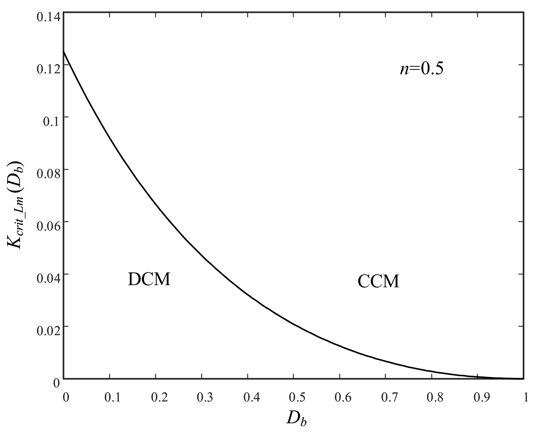
4.4. Boundary Curve of Lm

For convenience of analysis, it is assumed that the input power Pin is identical to the output power Po, that the input power is separated, and that the input currents for the two thermoelectric generators are the same, namely, Iin1 = Iin2 = Iin. At the same time, from Figure 5, it can be seen that the average current is zero for the charge pump capacitors C2 and C3. Therefore, the average current in the secondary-side winding, INs, is identical to the average current in the output inductor, ILo. Figure 12 shows the equivalent model for the DC current analysis of the coupled inductor.
According to state 2 and (5), the primary-side voltage vNp can be expressed as follows:
v N p = v L m = V i n 2 + V C 1
Since there is no power loss in the circuit, the resulting equation can be attained as:
P i n = P o = V o × I o
Rearranging (29) yields:
V o × I o = ( V i n 2 + V C 1 ) × I i n
where:
I o = V o R o
From Figure 12, the average current of iLm can be represented by:
I L m = I N p + I i n
and:
I N p = I N s n = I o n
Rearranging (30) yields:
I i n = V o V i n 2 + V C 1 × I o
Substituting (18) and (28) into (34) yields:
I i n = 2 n × ( D b 1 D b ) × I o
Substituting (33) and (35) into (32) yields:
I L m = I o n 1 + D b 1 D b
Substituting (31) into (36) yields:
I L m = V o n R o 1 + D b 1 D b
In addition, the ripple current of i L m , Δ i L m , can be obtained as follows:
Δ i L m = v L m × Δ t L m
Substituting (28) into (38) yields:
Δ i L m = V i n 2 + V C 1 L m D b T s
Therefore, as 2 I L m Δ i L m , the magnetizing inductance Lm will operate in CCM; that is:
2 I L m Δ i L m 2 × 2 V o n R o 1 + D b 1 D b V i n 2 + V C 1 L m D b T s 2 L m R o T s n × V i n 2 + V C 1 V o × D b 1 + D b 1 D b 2 L m R o T s n × n ( 1 D b ) 2 D b × D b 1 + D b 1 D b 2 L m R o T s n 1 D b 2 2 ( 1 + D b ) K L m K c r i t _ L m ( D b )
where K L m = 2 L m R o T s and K c r i t _ L m ( D b ) = n 1 D b 2 2 ( 1 + D b ) .
From (40), under the turns ratio n = 0.5, if K L m K c r i t _ L m ( D b ) holds, the inductance Lm will operate in CCM; if not, Lm will work in DCM. Accordingly, the boundary curve between CCM and DCM can be drawn as shown in Figure 13.

4.5. Boundary Condition for Lo

The average current of the output inductor ILo is identical to the output current Io, namely:
I L o = I o
Additionally:
I o = V o R o
According to (41), and by substituting (20) into (42), the following equation can be expressed:
I L o = 2 n V i n 2 + V i n 1 D a 1 D a D b 1 D b R o
Moreover, the ripple current of i L o , represented as Δ i L o , can be obtained as follows:
Δ i L o = v L o × Δ t L o
Substituting (4) into (44) yields:
Δ i L o = 1 n ( V i n 2 + V C 1 ) + V C 2 + V C 3 V o L o D b T s
Substituting (16) and (20) into (45) yields:
Δ i L o = 1 n V i n 2 + D a 1 D a V i n 1 L o D b T s
Substituting (4) into (25) yields:
Δ i L = V i n 1 L D a T s
Therefore, as 2 I L o Δ i L o , the output inductor Lo operates in CCM; that is:
2 × 2 n V i n 2 + V i n 1 D a 1 D a D b 1 D b R o 1 n V i n 2 + D a 1 D a V i n 1 L o D b T s 2 L o R o T s ( 1 D b ) 2 K L o K c r i t _ L o ( D b )
where K L o = 2 L o R o T s and K c r i t _ L o ( D b ) = ( 1 D b ) 2 .
From (48), it can be known that if K L o K c r i t _ L o ( D b ) holds, the output inductor Lo works in CCM; if not, Lo operates in DCM. Therefore, the boundary curve between CCM and DCM can be sketched as shown in Figure 14.

4.6. Topology Extension

As displayed in Figure 15, the proposed converter can be expanded to N inputs, where N is a positive integer; hence, its input count will be increased such that the thermal energy from all of the sources can be recycled.

5. Design Considerations

5.1. Thermoelectric Module Specifications

The thermoelectric modules adopted herein are called TGM-199-1.4-0.8, made by Kryotherm Co. There are two inputs in the proposed converter: the first input is fed by four series-connected thermoelectric modules, while the second input is fed by two series-connected thermoelectric modules. The associated specifications are displayed in Table 1 and Table 2.

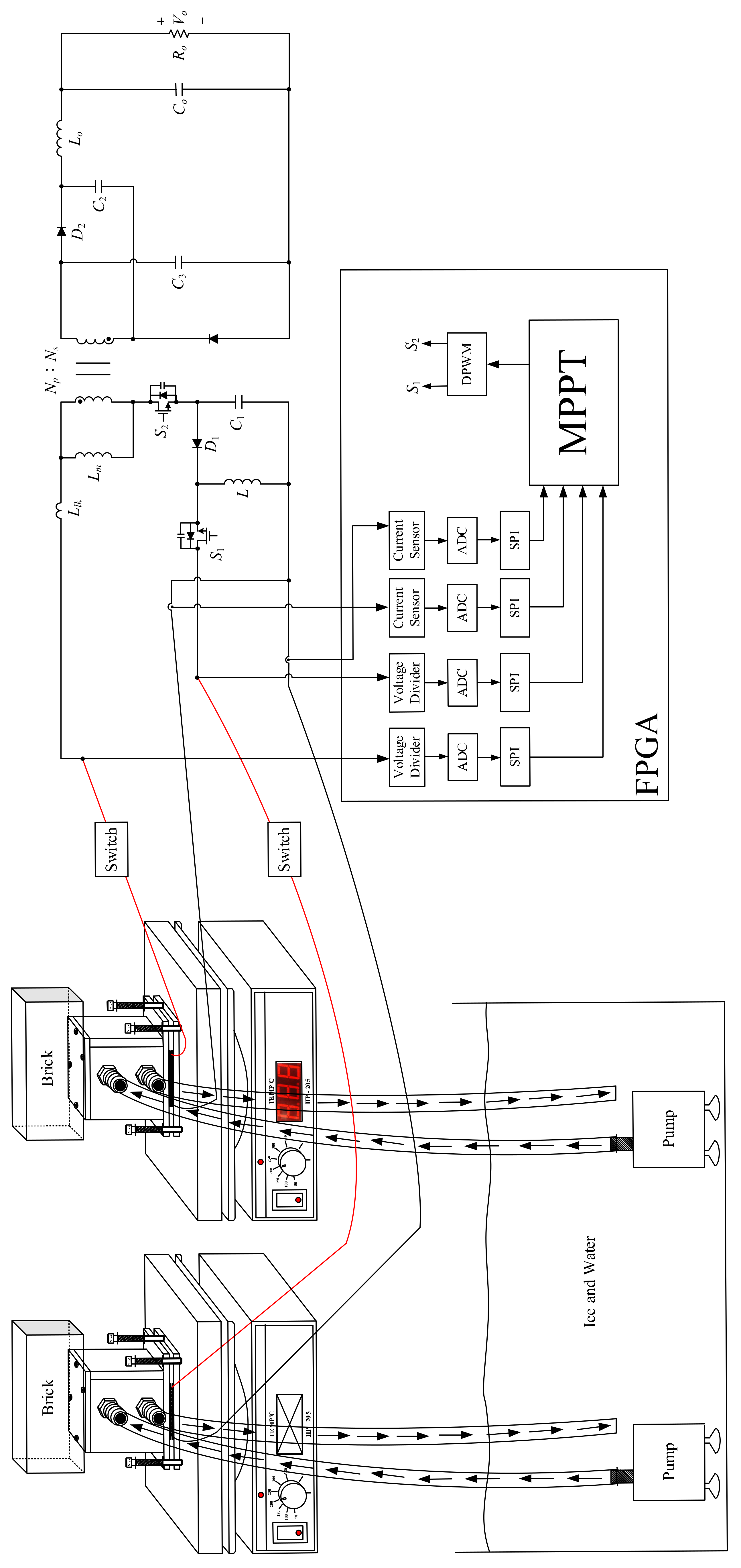
5.2. System Configuration Together with Design Concept and Experimental Strategy

Figure 16 shows the proposed isolated MISOC converter along with two thermoelectric generators, with an FPGA control kernel. According to Table 1 and Table 2, the first TEG under MPPT has an output voltage of 14 V, and its output current is 1.653 A, whereas the second TEG under the MPPT has an output voltage of 7.5 V and an output current of 1.56 A. Therefore, the sum of the power generated from the two TEGs is 34.88 W. Accordingly, based on the above-mentioned factors, and by prescribing the output voltage of the converter at 100 V, Table 3 and Table 4 display the system specifications and the respective converter specifications. An efficiency curve can be attained under the output voltage regulated at 100 V. Afterwards, the MPPT algorithm is imposed on this converter to harvest thermal energy; hence, some waveforms are measured. Moreover, under the control of MPPT, the needed digital signals—containing the input voltages and currents—are created after the analog-to-digital converters (ADCs), the field-programmable gate array (FPGA) shown in Table 5 is utilized to control such a system, and the gate-driving signals generated by the FPGA are passed to the switches. Note that since this circuit focuses on harvesting thermal energy, the output voltage sensor and the corresponding voltage mode controller are not displayed in Figure 16.

5.3. Calculation of Duty Cycles

Based on (39), with Da equal to 0.6, the value of Db will be calculated to be 0.4975.
V o = 2 n V i n 2 + V i n 1 D a 1 D a D b 1 D b 100 = 2 0.5 14 + 7.5 0.6 1 0.6 D b 1 D b D b = 0.4975

5.4. Design of L

By assuming that the inductor L works in CCM above 0.1 Immp1, and according to the following equation, the value of Lmin can be derived as follows:
L m i n = v L × D a × T s 2 × 0.1 I m p p 1 ÷ D a = 7.5 × 0.6 2 × 10 μ 2 × 0.1 × 1.56 = 86.54   μ H
Eventually, the value of L is set at 100 μH.

5.5. Design of Lo

By assuming that the inductor Lo works in CCM above Io,min, and according to the following equations, the value of Lo,min can be derived as follows:
v L o = 1 n V i n 2 + D a 1 D a V i n 1 = 1 0.5 14 + 0.6 1 0.6 × 7.5 = 50.5   V
L o , m i n = v L o × D b × T s 2 × I o , min = 50.5 × 0.4975 × 10 μ 2 × 34.88 m = 3.6 mH
Eventually, the value of Lo is set at 4.32 mH.

5.6. Design of Lm

By assuming that the inductor Lm operates in CCM above Io,min, and according to (40), the value of Lm,min can be derived as follows:
L m , m i n = n 1 D b 2 4 ( 1 + D b ) × T s × V o I o , m i n = 0.5 1 0.4975 2 4 ( 1 + 0.4975 ) × 10 μ × 100 34.88 m = 302   μ H
Eventually, the value of Lm is set at 330 μH.

5.7. Design of C1

By assuming that the maximum ripple voltage of C1 is 1% of VC1, and based on the following equations, the value of C1,min can be worked out as follows:
V C 1 = D a 1 D a × V i n 1 = 0.6 1 0.6 × 7.5 = 11.25   V
C 1 , m i n = I i n D a × ( 1 D a ) T s 0.01 × V C 1 = 1.56 0.6 × ( 1 0.6 ) 10 μ 0.01 × 11.25 = 92   μ F
Eventually, the value of C1 is set at 150 μF.

5.8. Design of C2 and C3

By assuming that the maximum ripple voltage of C2 or C3 is 0.1% of VC2 or VC3, respectively, and based on (17), the value of C2,min or C3,min can be worked out as follows:
V C 2 = V C 3 = 1 n ( V i n 2 + V C 1 ) D b 1 D b = 1 0.5 ( 14 + 11.25 ) 0.4975 1 0.4975 = 50   V
C 2 , m i n = C 3 , m i n = I o , r a t e d × ( 1 D b ) T s 0.001 × V C 2 = 0.3488 × ( 1 0.4975 ) × 10 μ 0.001 × 50 = 35.1   μ F
Finally, the value of C2 or C3 is set at 47 μF.

5.9. Design of Co

By assuming that the maximum ripple voltage of Co is 0.1% of VCo, and based on [21], the value of Co,min can be worked out as follows:
Δ i L o = 1 n ( V i n 2 + V C 1 ) × D b × T s ÷ L o = 1 0.5 × ( 14 + 11.25 ) × 0.4975 × 10 μ ÷ 4.32 m = 0.0587   A
E S R = 0.001 × V o Δ i L o = 0.001 × 100 0.0587 = 1.704   Ω
E S R × C o , m i n = 50 ~ 80 μ C o , m i n = 80 μ 1.704 = 46.08   μ F
Eventually, the value of Co is set at 68 μF.

5.10. Converter Topology Comparison

In Table 6, two circuits shown in [19] and [20] are employed as comparisons. The number of components is used as a comparison item, to be described below. From Table 6, it can be seen that the proposed converter has the smallest number of components.

6. Simulated and Experimental Results

6.1. Simulated Results

A PSIM-based simulation was utilized to demonstrate the feasibility of this system with the designed resistance of 313 Ω (100 V/348 mA) used as a load. Since in the PSIM software only a solar cell model can be utilized, the parameters of this model were modified to simulate TEG operation. There are three examples to be discussed, as follows:
In example 1, displayed in Figure 17, it can be seen that the generated power relevant to TEG1 is 22.976 W, and this value is close to the MPP power of 23.142 W, while the generated power relevant to TEG2 is 11.029 W, and this value is close to the MPP power of 11.7 W. Summing the two powers yields 34.005 W, and this value is almost the same as the output power of 34.065 W. Moreover, the output voltage is 98.81 V, which is close to 100 V. In addition, the corresponding duty cycles of Dc and Dd are 0.578 and 0.52, respectively, and these values are somewhat different from 0.6 and 0.4975 under voltage mode control, respectively.
In example 2, displayed in Figure 18, the short current Isc of TEG1 is three times that of TEG1 in Figure 17. From Figure 18, it can be seen that the generated power relevant to TEG1 is 67.004 W, and this value is close to the MPP power of 69.426 W, while the generated power relevant to TEG2 is 10.45 W, and this value is close to the MPP power of 11.7 W. Summing the two powers yields 77.454 W, and this value is close to the output power of 76.835 W. Moreover, the output voltage is 148.39 V, and this is because the more the power is transferred, the higher the output voltage.
In example 3, displayed in Figure 19, the open voltage Voc of TEG1 is four times that of TEG1 in Figure 17. From Figure 19, it can be seen that the generated power relevant to TEG1 is 85.951 W, and this value is close to the MPP power of 85.956 W, while the generated power relevant to TEG2 is 11.28 W, and this value is close to the MPP power of 11.7 W. Summing the two powers yields 97.231 W, and this value is close to the output power of 93.81 W. Moreover, the output voltage is 163.97 V, and this is because the more the power is transferred, the higher the output voltage.

6.2. Efficiency Curve

An efficiency curve can be attained under the output voltage regulated at 100 V, with the electronic load working in the constant current (CC) mode. From Figure 20, it can be seen that the efficiency at 10% load is ~72.2%, the efficiency at 100% load is ~85.2%, and the maximum efficiency is ~87.2%. The reason that the efficiency is not high is the low current in the load.

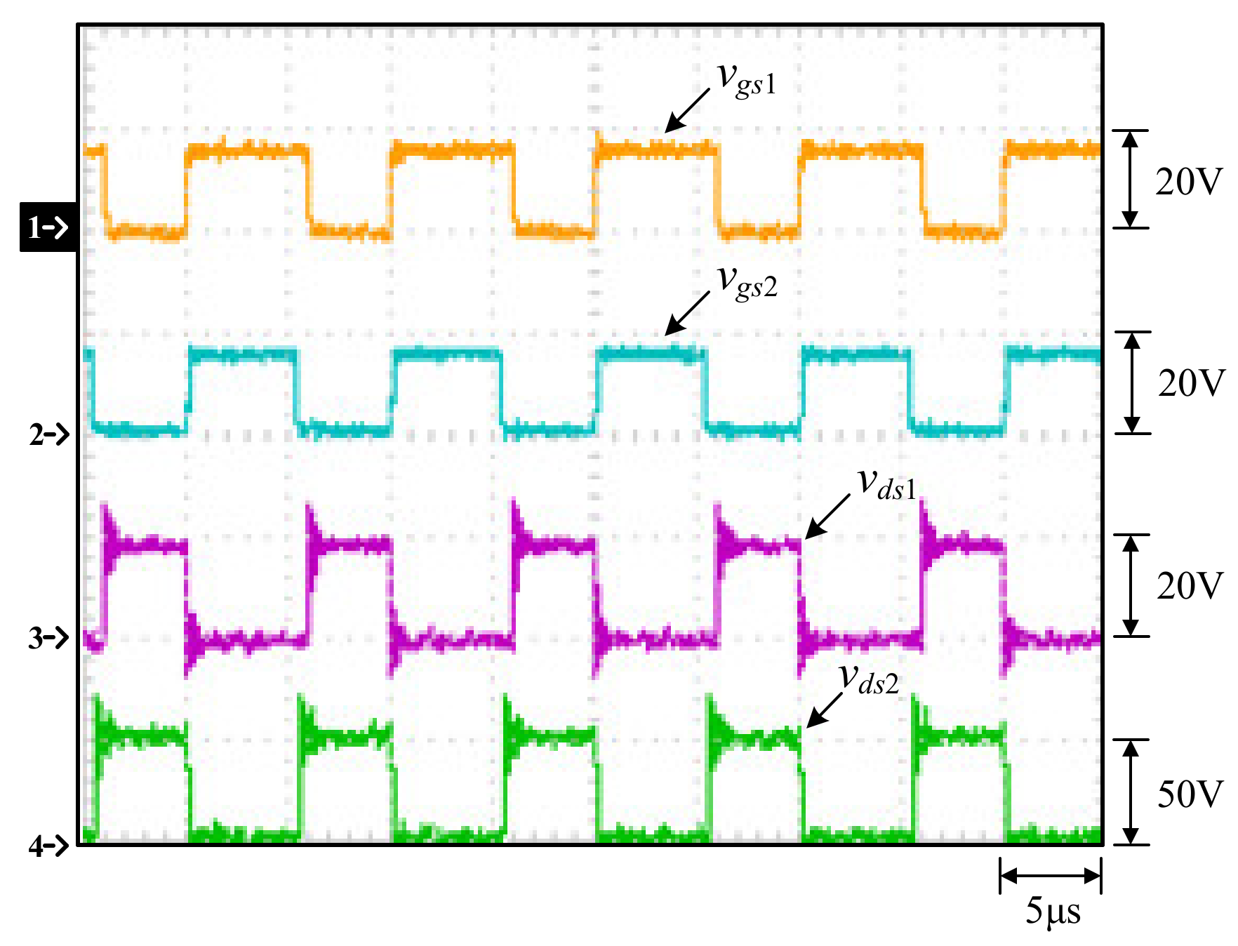
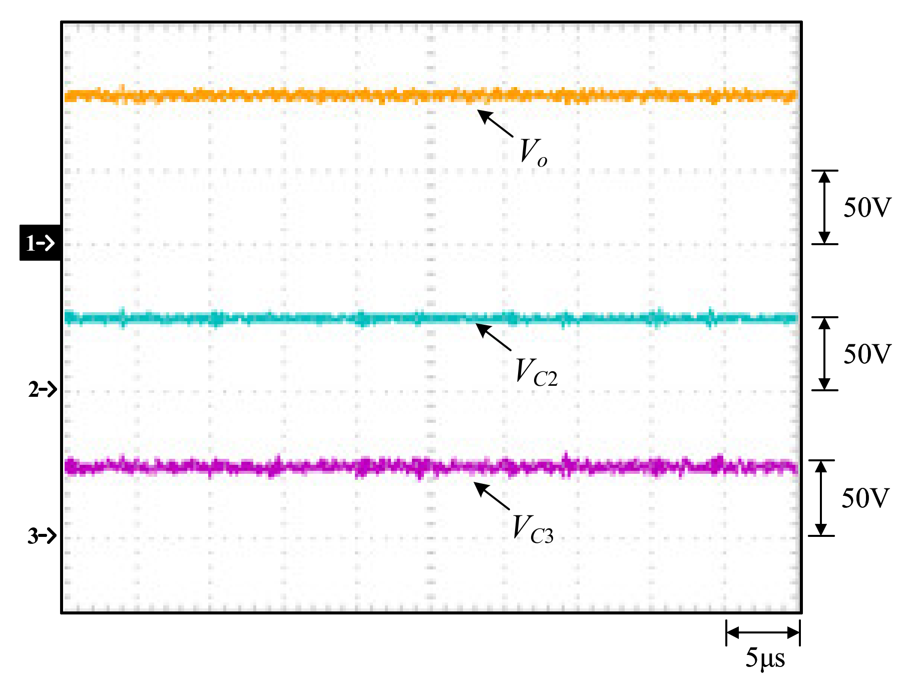
6.3. Measured Waveforms

After the efficiency curve is finished, the MPPT algorithm is applied to the proposed converter to demonstrate the maximum power transfer, with some illustrated waveforms given. Note that for MPPT experiments, an electronic load works in the constant voltage (CV) mode.
In the following section, the waveforms shown from Figure 21, Figure 22, Figure 23, Figure 24, Figure 25 and Figure 26 are measured under MPPT. Figure 21 shows the gate-driving signals vgs1 and vgs2 for S1 and S2, respectively, and the voltages across S1 and S2, called vds1 and vds2, respectively; Figure 22 displays the gate-driving signal vgs1 for S1, the voltage across D1, the current flowing through L—represented as iL—and the voltage across C1; Figure 23 shows the gate-driving signal vgs2 for S2, and the voltages across D2 and D3, represented as vD2 and vD3, respectively; Figure 24 displays the gate-driving signal vgs2 for S2, the input current iin2, the secondary-side current iNs, and the output current iLo; Figure 25 shows the output voltage Vo, and the voltages across C2 and C3, represented as VC2 and VC3, respectively; Figure 26 displays the output voltage Vo, and the input voltages Vin1 and Vin2, which are created from TEG1 and TEG2, respectively.
From Figure 21, it can be seen that the maximum voltages across S1 and S2 are approximately 20 V and 50 V, respectively. From Figure 22, it can be seen that the maximum voltage across the diode D1 is ~25 V, with high-frequency oscillation due to the parasitic capacitance of D1 resonating with the line parasitic inductance, while the voltage across C1 is ~13 V, and the average value of iL is ~2.3 A, implying that the average value of iin1 is ~1.6 A, and that TEG1 works at MPP. From Figure 23, it can be seen that the maximum voltages across the diodes D2 and D3 are ~100 V, with high-frequency oscillation due to the parasitic capacitances of D2 and D3 resonating with the line parasitic inductance and the secondary-side leakage inductance Llk2. From Figure 24, it can be seen that the average value of iLo is 350 mA, and the average value of iin2 is ~1.5 A, implying that TEG2 works at MPP. Figure 25 shows that the value of Vo is ~100 V, while the values of VC2 and VC3 are ~50 V, meaning that the voltages across the two capacitors C2 and C3 can be kept constant at the desired value. Figure 26 shows that the value of Vo is ~100 V, the value of Vin1 is ~7.5 V, and the value of Vin2 is ~14 V, implying that the two TEGs operate under individual MPPs. Figure 27 shows photos of the proposed thermoelectric system containing the MISOC circuit and the thermoelectric platform.

7. Conclusions

The presented isolated MISOC circuit was analyzed and imposed on a one-stage thermal energy harvesting system. In this system, TEGs possess individual MPPT functions, thus rendering the thermal energy harvesting more efficient. Moreover, the presented converter has a relatively high step-up ratio. Furthermore, the input count can be increased, indicating that more TEGs can be connected to such a converter with individual MPPT functions. Finally, future works should aim to increase the power level along with the soft switching technology applied.

Author Contributions

Conceptualization, Y.-T.Y. and K.-I.H.; methodology, Y.-T.Y.; software, J.-J.S.; validation, Y.-T.Y., K.-I.H. and J.-J.S.; formal analysis, Y.-T.Y.; investigation, J.-J.S.; resources, Y.-T.Y.; data curation, J.-J.S.; writing—original draft preparation, K.-I.H.; writing—review and editing, K.-I.H.; visualization, J.-J.S.; supervision, K.-I.H.; project administration, K.-I.H.; funding acquisition, J.-J.S. All authors have read and agreed to the published version of the manuscript.

Funding

This research was funded by the Ministry of Science and Technology, Taiwan, under the Grant Number: MOST 110-2221-E-035-050.

Institutional Review Board Statement

Not applicable.

Informed Consent Statement

Not applicable.

Data Availability Statement

No new data were created or analyzed in this study. Data sharing is not applicable to this article.

Conflicts of Interest

The authors declare no conflict of interest.

References

  1. Karpe, S. Thermoelectric power generation using waste heat of automobile. Int. J. Curr. Eng. Technol. 2016, 4, 144–148. [Google Scholar]
  2. Testa, A.; De Caro, S.; Scimone, T.; Cacciato, M.; Scelba, G. A NPC step-up inverter for thermo-electric generators. In Proceedings of the 2015 International Conference on Clean Electrical Power (ICCEP), Taormina, Italy, 16–18 June 2015; pp. 780–785. [Google Scholar] [CrossRef]
  3. John, J.; Jose, J. A new three phase step up multilevel inverter topology for renewable energy applications. In Proceedings of the 2016 International Conference on Circuit, Power and Computing Technologies (ICCPCT), Nagercoil, India, 18–19 March 2016; pp. 1–5. [Google Scholar] [CrossRef]
  4. Sanz, A.; Vidaurrazaga, I.; Pereda, A.; Alonso, R.; Roman, E.; Martinez, V. Centralized vs. distributed (power optimizer) PV system architecture field test results under mismatched operating conditions. In Proceedings of the 2011 37th IEEE Photovoltaic Specialists Conference, Seattle, WA, USA, 19–24 June 2011; pp. 2435–2440. [Google Scholar] [CrossRef]
  5. Liu, Y.-C.; Chen, Y.-M. A systematic approach to synthesizing multi-input DC–DC converters. IEEE Trans. Power Electron. 2009, 24, 116–127. [Google Scholar] [CrossRef]
  6. Lam, J.; Jain, P.K. A novel electrolytic capacitor-less multi-input DC/DC converter with soft-switching capability for hybrid renewable energy system. In Proceedings of the 2014 16th European Conference on Power Electronics and Applications, Lappeenranta, Finland, 26–28 August 2014; pp. 1–10. [Google Scholar] [CrossRef]
  7. Haghighian, S.K.; Hosseini, S.H. A novel multi-input DC/DC converter with a general power management strategy for grid connected hybrid PV/FC/battery system. In Proceedings of the 6th Power Electronics, Drive Systems and Technologies Conference (PEDSTC2015), Tehran, Iran, 3–4 February 2015; pp. 1–6. [Google Scholar] [CrossRef]
  8. Lara-Salazar, G.; Vázquez, N.; Hernández, C.; López, H.; Arau, J. Multi-input DC/DC converter with battery backup for renewable applications. In Proceedings of the 2016 13th International Conference on Power Electronics (CIEP), Guanajuato, Mexico, 20–23 June 2016; pp. 47–51. [Google Scholar] [CrossRef]
  9. Akar, F. A high-efficiency bidirectional non-isolated multi-input converter. In Proceedings of the 2016 19th International Symposium on Electrical Apparatus and Technologies (SIELA), Bourgas, Bulgaria, 29 May–1 June 2016; pp. 1–4. [Google Scholar] [CrossRef]
  10. Delshad, M.; Harchegani, A.T.; Karimi, M.; Mahdavi, M. A new ZVT multi-input converter for hybrid sources systems. In Proceedings of the 2016 International Conference on Applied Electronics (AE), Pilsen, Czech Republic, 6–7 September 2016; pp. 61–64. [Google Scholar] [CrossRef] [Green Version]
  11. Zhang, N.; Sutanto, D.; Muttaqi, K.M. A buck-boost converter based multi-input DC-DC/AC converter. In Proceedings of the 2016 IEEE International Conference on Power System Technology (POWERCON), Wollongong, NSW, Australia, 28 September–1 October 2016; pp. 1–6. [Google Scholar] [CrossRef]
  12. Poshtkouhi, S.; Trescases, O. Multi-input single-inductor dc-dc converter for MPPT in parallel-connected photovoltaic applications. In Proceedings of the 2011 Twenty-Sixth Annual IEEE Applied Power Electronics Conference and Exposition (APEC), Fort Worth, TX, USA, 6–11 March 2011; pp. 41–47. [Google Scholar] [CrossRef]
  13. Baddipadiga, B.P.; Ferdowsi, M. A high-voltage-gain dc-dc converter based on modified Dickson charge pump voltage multiplier. IEEE Trans. Power Electron. 2016, 32, 7707–7715. [Google Scholar] [CrossRef]
  14. Jiang, W.; Fahimi, B. Maximum solar power transfer in multi-port power electronic interface. In Proceedings of the 2010 Twenty-Fifth Annual IEEE Applied Power Electronics Conference and Exposition (APEC), Palm Springs, CA, USA, 21–25 February 2010; pp. 68–73. [Google Scholar] [CrossRef]
  15. Hwu, K.I.; Jiang, W.Z. Analysis, design and derivation of a two-phase converter. IET Power Electron. 2015, 8, 1987–1995. [Google Scholar] [CrossRef]
  16. Hwu, K.-I.; Yau, Y.-T.; Hsieh, M.-L. Thermoelectric energy conversion system with multiple inputs. IEEE Trans. Power Electron. 2019, 35, 1603–1621. [Google Scholar] [CrossRef]
  17. Khosrogorji, S.; Torkaman, H.; Karimi, F. A short review on multi-input DC/DC converters topologies. In Proceedings of the 6th Power Electronics, Drive Systems and Technologies Conference (PEDSTC2015), Tehran, Iran, 3–4 February 2015; pp. 650–654. [Google Scholar] [CrossRef]
  18. Li, Y.; Ruan, X.; Yang, D.; Liu, F.; Tse, C.K. Synthesis of multiple-input DC/DC converters. IEEE Trans. Power Electron. 2010, 25, 2372–2385. [Google Scholar] [CrossRef]
  19. Lam, J.; Jain, K. An asymmetrical PWM (APWM) controlled multi-input isolated resonant converter with zero voltage switching (ZVS) for hybrid renewable energy systems. In Proceedings of the 2014 IEEE 36th International Telecommunications Energy Conference (INTELEC), Vancouver, BC, Canada, 28 September–2 October 2014; pp. 1–6. [Google Scholar] [CrossRef]
  20. Zeng, J.; Qiao, W.; Qu, L. An isolated multiport DC-DC converter for simultaneous power management of multiple renewable energy sources. In Proceedings of the 2012 IEEE Energy Conversion Congress and Exposition (ECCE), Raleigh, NC, USA, 15–20 September 2012; pp. 3741–3748. [Google Scholar] [CrossRef]
  21. Nilsson, J.W.; Riedel, S. Electric Circuits, 10th ed.; Pearson Education Inc.: London, UK, 2005. [Google Scholar]
  22. Laird, I.; Lu, D.D.-C. High step-up DC/DC topology and MPPT algorithm for use with a thermoelectric generator. IEEE Trans. Power Electron. 2012, 28, 3147–3157. [Google Scholar] [CrossRef]
Figure 1. Deduction of the TEG MPP.
Energies 15 00273 g001
Figure 2. TEG P–I–V Curves.
Energies 15 00273 g002
Figure 3. Operating procedure of the three-point weighting strategy for MPPT.
Energies 15 00273 g003
Figure 4. Three cases for the three-point weighting strategy. (a), Pa > Pb > Pc; (b), Pa < Pb < Pc; (c), Pb > Pa and Pc.
Energies 15 00273 g004
Figure 5. Proposed isolated MISOC circuit.
Energies 15 00273 g005
Figure 6. Illustrated waveforms relevant to the proposed isolated MISOC circuit.
Energies 15 00273 g006
Figure 7. State 1 power flow.
Energies 15 00273 g007
Figure 8. State 2 power flow.
Energies 15 00273 g008
Figure 9. State 3 power flow.
Energies 15 00273 g009
Figure 10. State 4 power flow.
Energies 15 00273 g010
Figure 11. Boundary curve between CCM and DCM for L.
Energies 15 00273 g011
Figure 12. Equivalent model for DC current analysis of the coupled inductor.
Energies 15 00273 g012
Figure 13. Boundary curve between CCM and DCM for Lm.
Energies 15 00273 g013
Figure 14. Boundary curve between CCM and DCM for Lo.
Energies 15 00273 g014
Figure 15. Expanded circuit.
Energies 15 00273 g015
Figure 16. Thermoelectric system with the proposed isolated MISOC.
Energies 15 00273 g016
Figure 17. Simulation example 1.
Energies 15 00273 g017
Figure 18. Simulation example 2.
Energies 15 00273 g018
Figure 19. Simulation example 3.
Energies 15 00273 g019
Figure 20. Curve of efficiency versus load current.
Energies 15 00273 g020
Figure 21. Waveforms measured under the thermoelectric system: (1) vgs1; (2) vgs2; (3) vds1; (4) vds2.
Energies 15 00273 g021
Figure 22. Waveforms measured under the thermoelectric system: (1) vgs1; (2) vD1; (3) iL; (4) VC1.
Energies 15 00273 g022
Figure 23. Waveforms measured under the thermoelectric system: (1) vgs2; (2) vD2; (3) vD3.
Energies 15 00273 g023
Figure 24. Waveforms measured under the thermoelectric system: (1) vgs2; (2) iin2; (3) iNs; (4) iLo.
Energies 15 00273 g024
Figure 25. Waveforms measured under the thermoelectric system: (1) Vo; (2) VC2; (3) VC3.
Energies 15 00273 g025
Figure 26. Waveforms measured under the thermoelectric system: (1) Vo; (2) Vin1; (3) Vin2.
Energies 15 00273 g026
Figure 27. Photos of the proposed thermoelectric system: (a) MISOC circuit; (b) thermoelectric platform.
Energies 15 00273 g027
Table 1. Specifications for the first thermoelectric module.
Part NameTGM-199-1.4-0.8
Size 40 × 40 × 3.2 mm
NumberFour in series
Maximum Power (Pmpp1)23.2 W
Voltage at MPP (Vmpp1)14 V
Current at MPP (Impp1)1.653 A
Open Voltage (Voc1)27.6 V
Short Current (Isc1)3.25 A
Cold-Side Temperature80 °C
Hot-Side Temperature180 °C
Table 2. Specifications for the second thermoelectric module.
Part NameTGM-199-1.4-0.8
Size 40 × 40 × 3.2 mm
NumberTwo in series
Maximum Power (Pmpp2)11.68 W
Voltage at MPP (Vmpp2)7.5 V
Current at MPP (Impp2)1.56 A
Open Voltage (Voc2)13.95 V
Short Current (Isc2)3.246 A
Cold-Side Temperature80 °C
Hot-Side Temperature180 °C
Table 3. System specifications.
Operating ModeCCM
First Input Voltage (Vin1)7.5 V
Second Input Voltage (Vin2)14 V
Rated Output Voltage (Vo)100 V
Rated Output Current (Io,rated)/Power (Po,rated)348.8 mA/34.88 W
Minimum Output Current (Io,min)/Power (Po,min)34.88 mA/3.488 W
Switching Frequency (fs)/Power (Ts)100 kHz/10 μs
n = Np/Ns0.5
Table 4. Component specifications used in the isolated MISOC.
ComponentsSpecifications
MOSFET Switch S1IRF3205 Z
MOSFET Switch S2STB120NF10T4
Diode D1STPS30L30CT
Diodes D2, D3STPS20H100CT
Charge Pump Capacitor C1150 μF Electrolytic Capacitor
Charge Pump Capacitors C2, C347 μF Electrolytic Capacitor
Output Capacitor Co68 μF Electrolytic Capacitor
Input Inductor L100 μH
Output Inductor Lo4.32 mH
Coupled InductorLm = 330 μH, n = 0.5
Isolated Gate DriverFOD3182
Table 5. EP3C5E144C8N specifications.
DeviceLogic
Elements
Total RAM Bits18 × 18
Multipliers
PLLsUser I/O Pins
EP3C5E144C8N513642393623294
Table 6. Comparison between the existing [19,20] and the proposed circuits.
Component No.[19][20]Proposed
Input222
Inductor332
Coupled Inductor211
Switch422
Diode453
Charge Pump Capacitor413
Publisher’s Note: MDPI stays neutral with regard to jurisdictional claims in published maps and institutional affiliations.

