Article

A Digital Delay Compensation Method to Improve the Stability of LCL Grid-Connected Inverters

1
Key Lab of Power Electronics for Energy Conservation and Motor Drive of Hebei Province, Yanshan University, Qinhuangdao 066004, China
2
Electric Power Research Institute of State Grid Hebei Electric Power Co., Ltd., Shijiazhuang 050021, China
*
Author to whom correspondence should be addressed.
Energies 2021, 14(9), 2730; https://doi.org/10.3390/en14092730
Submission received: 26 March 2021 / Revised: 30 April 2021 / Accepted: 4 May 2021 / Published: 10 May 2021
(This article belongs to the Section A1: Smart Grids and Microgrids)

Abstract

:
Grid-connected inverters are an important part of the connection between distributed power generation units and the large grid, and their stability is the basis for ensuring the safe operation of distributed power generation units. This study found that there is an inherent digital control delay in the three-phase LCL grid-connected inverter system. This characteristic causes the effective range of capacitive current feedback active damping to be reduced, the selection range of the active damping coefficient to be limited, and the phase at the open-loop cutoff frequency to be reduced. In order to reduce the impact of digital delay, this article conducts a detailed analysis of the characteristics of the first-order lead link that can be used as delay compensation, pointing out that its infinite gain when it obtains the optimal compensation effect will bring noise to the inverter system. This paper proposes a method of cascading digital filters for the first-order leading link to suppress its infinite gain. An improved delay compensation link that is more suitable for numerically controlled inverter systems is constructed. Finally, the effectiveness and necessity of the proposed improved delay compensation link are verified by a simulation platform and an experimental platform.

1. Introduction

LCL-type grid-connected inverters have the advantage of a better harmonic filtering effect; as such, the stability of LCL-type grid-connected inverters has been studied and given attention by many scholars [1,2]. The third-order undamped nature of the LCL filter will cause the Bode plot of the grid-connected inverter system to cross the −180° line when the gain is greater than zero. In order to avoid this situation, a method of adding passive damping in the hardware or adding active damping in the control loop is usually chosen to suppress the infinite gain at the resonant frequency of the filter. Compared with passive damping [3], active damping has received more attention and been given more applications due to its flexible implementation and the advantages of not causing energy waste [4,5,6,7,8]. Among such methods, the active damping method based on capacitive current feedback is widely used [5,6,7,8].
Through appropriate filter design and the filter capacitor series active damping method, filter resonance can be suppressed, and a good steady-state error and fast dynamic response can be achieved through simple PI control [9]. Pan et al. [10] effectively reduces the harmonic content of the output current through the LCL filter designed by magnetic integration. However, Sgrò et al. [9] and Pan et al. [10] did not analyze the influence of the selection of the active damping coefficient and the delay of digital control on the effective range of active damping.
Due to the equivalent delay in digital control, the equivalent impedance of capacitive current feedback active damping changes with the change of frequency [11], and its effective range of resonance spike suppression is reduced. In order to improve this nature, many scholars have put forward their personal hypotheses. The effective range of the capacitive current feedback active damping method is expanded when reducing the effect of the equivalent delay in digital control. Some design methods have been proposed: for example, changing the capacitive current proportional feedback to proportional integral feedback [12,13]. The leading link with delay compensation is used to replace the proportional link in the controller [14]. The delay compensation method based on the state estimation method is used to reduce the influence of the digital delay on the active damping properties [15]. Liu et al. [16] proposed a second-order lead–lag link delay compensation function, but the compensation function is proposed in the continuous domain, which is more cumbersome for digital realization.
Lu et al. [17] describes the principle and performance of four delay compensation links. On this basis, various delay compensation methods are proposed. For example, using the delay compensation method based on additional area insertion, using the delay compensation method based on the principle of area equivalence [18], using the phase advance link to compensate for the digital delay [19], adding a first-order advance link with phase advance properties to the forward channel of the control loop [20], and reducing the impact of digital delay by adding a second-order lead link with phase lead to the capacitive current feedback channel [21]. The second-order lead link used in Liu et al. [21] is the square form of the first-order lead link, its gain in the middle and low frequency bands is almost zero, and it has the nature of phase lead. However, Chen et al. [18], Yang et al. [19] and Liu et al. [21] does not consider the nature of the first-order lead link in the high frequency band, especially near the Nyquist frequency. In Wang et al. [20], the method of reducing the delay compensation effect is adopted to avoid the infinite gain of the first-order lead link near the Nyquist frequency.
Aiming at the influence of digital delay on the effective range of active damping and the noise problem introduced by delay compensation, this paper has conducted the following work. First, this paper establishes a three-phase LCL grid-connected inverter system model based on digital control. The influence of inherent delay in digital control on active damping and the influence of active damping on the phase properties of the grid-connected system near the filter resonance frequency are analyzed in detail. Second, the characteristics of the first-order leading link of delay compensation are analyzed, pointing out that its infinite gain at the Nyquist frequency will bring noise pollution to the inverter system. Most importantly, this paper constructs an improved delay compensation link that is more suitable for digital control grid–connected inverter systems by cascading zero-phase-shift digital filters. While this link extends the effective range of active damping, it does not affect the amplitude of the grid-connected inverter system, avoids noise at the Nyquist frequency, and improves the stability of the system. Finally, the validity of the theoretical analysis is verified through a simulation platform and an experimental platform.

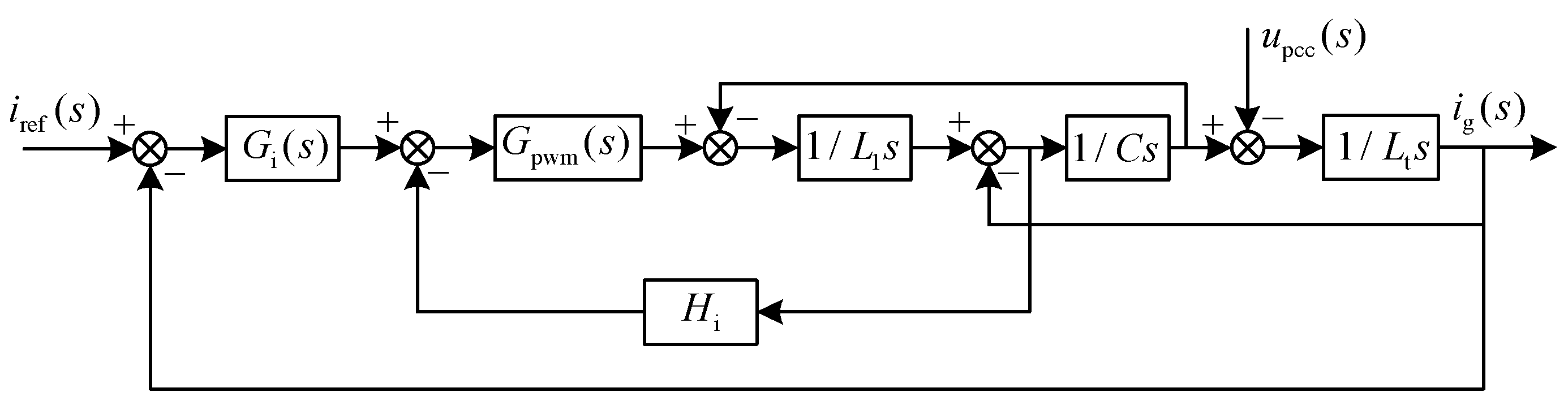
2. Three-Phase LCL-Type Grid-Connected Inverter System Model

First, a three-phase LCL grid-connected inverter system model is established under digital control, as shown in Figure 1. The hardware circuit mainly includes a three-phase bridge inverter circuit, an LCL filter, and a sampling circuit. The software portion mainly includes the coordinate transformation of the sampled value, the realization of the control algorithm, and the generation of the control signal SPWM. In the αβ-frame, the control system does not need decoupling and can reduce the influence of the phase-locked loop on the control loop. Therefore, this paper has chosen to design the inverter in the αβ-frame.
The equivalent delay time in digital control can be expressed as
G d e 1.5 T s s
where Ts represents the value of the sampling period. The modulation method of the bipolar symmetric regular sampling method is adopted in this article, and the sampling period is consistent with the switching period setting.
In Figure 1, UDC represents the input voltage on the DC side of the inverter; iabc/c represents the amount of three-phase capacitor current; uabc/c represents the amount of three-phase voltage at the PCC; Zg represents the equivalent grid impedance on the transmission line (because the resistance component in the grid impedance is beneficial to the stability of the inverter system, this article only considers the inductance part.); iabc/g represents the grid current value of the inverter; uabc/g represents the three-phase grid voltage; θ is the phase output value of the phase lock link; and idg/ref and iqg/ref represent the current reference value in the dq-frame given by the power loop. In the case of the unity power factor, iqg/ref = 0, idg/ref and iqg/ref undergo frame transformation to become the current reference value in the αβ-frame.
Gpwm can be expressed as
Gpwm(S) = Kpwm × Gd = K pwm× e−1.5TsS
where Kpwm represents the ratio of the DC side input voltage to the carrier gain and Hi is the capacitive current feedback active damping coefficient. Gi(s) is the quasi-resonant (QPR) controller and can be expressed as
G i ( s ) = K p + 2 K r ω i s s 2 + 2 ω i s + ω 0 2
where Kp is the proportional coefficient, Kr is the resonance coefficient, and ω0 is the fundamental angular frequency, whose value is 100π. ωi determines the bandwidth of the controller. In order to ensure that the grid current still has a small steady-state error when the fundamental frequency fluctuates ±0.5 Hz, ωi = π is often selected. Excluding the fundamental frequency, the QPR controller can be regarded as a purely proportional link [22].
The α-axis control block diagram is shown in Figure 2.
iref represents the reference value of the grid current of the α-axis and Lt represents the sum of the grid-connected side inductance of the filter and the inductance in the grid impedance. According to Figure 2, the open-loop transfer function of the α-axis can be expressed as
G ( s ) = G i ( s ) G pwm L 1 L t C s 3 + G pwm H i L t C s 2 + ( L 1 + L t ) s

3. The Influence of Digital Delay on Active Damping Characteristics

3.1. Active Damping Characteristics under Digital Control

Let the denominator of the open-loop transfer function in Equation (4) be N.
N can be expressed as
N = L 1 L t C s 3 + G pwm H i L t C s 2 + ( L 1 + L t ) s
Carrying out the Euler transformation of Equation (2) and introducing Equation (5), the result is
N = s ( ( L 1 + L t ) + A sin ( 1.5 ω T s ) ) + B cos ( 1.5 ω T s ) + s 3 L 1 L t C
where
A = K pwm H i L t C ω ,   B = K pwm s 2 H i L t C
When the imaginary part of Equation (6) is zero, the inverter system resonates. At this time, the absolute value of the coefficient of the first-order term and the coefficient of the third-order term are equal:
( L 1 + L t ) ω + K pwm H i L t C ω 2 × sin ( 1.5 ω T s ) L 1 L t C ω 3 = 0
According to Equation (7), the actual resonance frequency of the inverter system can be derived as
ω r = ( L 1 + L t ) + K pwm H i L t C ω × sin ( 1.5 ω T s ) L 1 L t C
The initial resonance frequency of the filter can be expressed as
ω res = ( L 1 + L t ) L 1 L t C
It can be seen from Equations (8) and (9) that the resonant frequency of the inverter system under digital control will be affected after active damping is added.
When KpwmHiLt × sin(1.5ωTs) > 0, the resonance frequency value increases; when KpwmHiLt × sin(1.5ωTs) < 0, the resonance frequency value decreases. When the active damping coefficient Hi is taken as a positive value, the change of the actual resonant frequency is determined by sin(1.5ωTs).
The reason why the LCL filter cannot be stable is that it is a third-order undamped system. The purpose of adding capacitive current feedback is to generate a damping term for the filter—that is, the quadratic term in the transfer function. Observing Equation (6), we can see that after adding capacitive current feedback active damping under digital control, the quadratic term in the transfer function is shown in Equation (10):
s 2 K pwm H i L t C × cos ( 1.5 ω T s )
With the change of ω, cos(1.5ωTs) will change the sign of the quadratic coefficient. According to the Routh criterion, the inverter system will become unstable when the quadratic coefficient is negative. To ensure the stability of the system, the value of cos(1.5ωTs) should always be positive.
From the above derivation, it can be seen that the equivalent delay will change the actual resonant frequency of the inverter system and affect the positive and negative coefficients of the quadratic term introduced by the capacitive current feedback, limiting the effective range of active damping. In the frequency range less than Nyquist, when the switching frequency fs is set to 20 kHz, the effect of the equivalent delay is shown in Table 1.
It can be seen from Table 1 that the coefficient of the quadratic term introduced by the capacitive current feedback is only positive at (0, 1/6fs). Active damping will only work when the actual resonant frequency is in this range. In the (0, 1/6fs) frequency band, the resonant frequency will increase due to the influence of the imaginary part of the capacitive current feedback. When the actual resonant frequency exceeds the effective area of active damping, the active damping will fail, and the inverter system will lose stability.
From a comparison of Equations (8) and (9), it can be seen that the magnitude of the resonant frequency shift is affected by the active damping coefficient Hi. When fres ∈ (0, 1/3fs), the greater the active damping coefficient, the greater the deviation of the resonance frequency. In order to make the actual resonant frequency value not exceed the effective area of active damping, the actual resonant frequency should be within (0, 1/6fs). At this time, according to Equation (8),
ω s 2 36 ( L 1 + L t ) + K pwm H i L t C ω s 6 × sin ( 1.5 ω s 6 T s ) L 1 L t C
Then, the value range of the active damping coefficient is obtained:
H i ω s 2 6 L 1 L t C 6 ( L 1 + L t ) K pwm L t C ω s
It can be seen that when fres ∈ (0, 1/3fs), the maximum value of the active damping coefficient should not exceed the limit of Equation (12).

3.2. The Influence of Active Damping on Properties near the Resonance Frequency

At the resonance frequency, the amplitude stability margin of the inverter system is required to be no less than GM. According to Equations (4) and (6), this can be expressed as
20 l g | G i ( s ) G pwm s 2 K pwm H i L t C × cos ( 1.5 ω r T s ) | GM 20 l g | K p K pwm ω r 2 K pwm H i L t C × cos ( 1.5 ω r T s ) | GM
At the initial resonance frequency, the amplitude can be expressed as
20 l g | G ( j ω res ) | = 20 l g K p K pwm | G pwm H i L t C ω res 2 | GM
Active damping changes the amplitude of the inverter system at the actual resonance frequency. Since |cos(1.5ωrTs)| ≤ 1 is always established, achieving the same amplitude margin at the actual resonant frequency as at the initial resonant frequency requires a larger active damping coefficient. According to Equation (12), it can be seen that an excessively large active damping coefficient will introduce unstable poles to the inverter system.
In order to clarify the influence of the change of the active damping coefficient on the inverter system, the Bode diagram of the open-loop transfer function under the values of the active damping coefficient of 0.04, 0.08, 0.12, 0.16, and 0.2 is plotted, as shown in Figure 3.
From Figure 3, considering the influence of digital delay with the gradual increase of the active damping coefficient, the offset of the resonance frequency also gradually increases. When the active damping coefficient exceeds a certain value, the phase of the transfer function changes significantly—that is, from crossing the −180° line once to crossing the −180° line twice.
In summary, a larger active damping coefficient will cause the actual resonant frequency to increase beyond the effective area of active damping. This will cause the inverter system to cross the −180° line negatively and positively at ωres and ωs/6, respectively. At this time, the inverter system has a sufficient gain margin at ωres and ωs/6, which is a necessary condition to ensure the stability of the grid-connected inverter system. Stability design becomes complicated and contradictory. In order to improve the design environment, the effect of the equivalent delay in digital control needs to be reduced.

4. Delay Compensation Link

4.1. First-Order Lead Link

The structure of the first-order lead link with phase lead properties is shown in Figure 4.
The transfer function of the first-order lead link can be expressed as
C ( s ) = m 1 + n × e k × T s s
The first-order lead link contains three coefficients: m, n, and k. Taking into account | e k × T s s | = 1 , in order to avoid the first-order lead link having an impact on the amplitude of the original system, the values of the coefficients m and n should satisfy the relationship of m = 1 + n.
In order to clarify the influence of each coefficient on the nature of the first-order lead link, Bode diagrams under different coefficient changes are drawn, as shown in Figure 5.
It can be seen from Figure 5a that when the other coefficients remain unchanged, the change of the coefficient m only changes the gain of the first-order lead link and has no effect on the phase. With the increase of the coefficient m, the gain of the first-order lead link gradually increases. Therefore, the coefficient m can play the role of first-order lead link gain correction.
It can be seen from Figure 5b that when m = 1 + n is satisfied, the change of the coefficient n can change the compensation effect for the delay—that is, the change of the coefficient n will affect the phase size of the first-order lead link. With the gradual increase of the coefficient n, the phase of the first-order lead link also gradually increases.
It can be seen from Figure 5c that no matter how the coefficients change, the first-order lead link will always have phase jumps and gain spikes at a certain frequency in the high frequency band. As the coefficient k increases, the frequency of the phase jump and gain spikes gradually decreases.

4.2. Improved Delay Compensation Link

The ideal time delay compensation link should only raise the phase of the original system without affecting the amplitude of the original system. In order to eliminate the infinite gain problem at the Nyquist frequency of the first-order lead link, a method of cascading low-pass filters is proposed. The traditional low-pass filter in the continuous domain has the effect of keeping the amplitude of the low frequency band unchanged, but the phase change occurs while attenuating the high-frequency signal. If the first-order lead link is cascaded with this type of low-pass filter, the compensation effect of the equivalent delay under digital control will definitely be affected.
The digital low-pass filter in Pan et al. [23] has the characteristic of being able to produce a large amplitude attenuation at the cut-off frequency and to maintain a gain of zero before the cutoff frequency. The choice of coefficients can ensure that its phase is always zero. Therefore, this article chooses the first-order lead link of the cascaded digital filter to construct an improved delay compensation link that is more suitable for the numerical control grid-connected inverter system. The newly constructed delay compensation link suppresses the infinite gain of the first-order lead link at the Nyquist frequency. The expression of the digital low-pass filter selected in this article is as follows:
Q i ( z ) = Z + a + Z 1 2 + a
As a continuous domain expression by Z = e T s , it can then be expressed as
Q i ( s ) = e T s + a + e T s 2 + a = 2 cos ( ω T ) + a 2 + a
It can be seen from Equation (17) that because cos(ωT) ∈ [–1, 1], if the coefficient a always satisfies a ≥ 2, then Qi(s) is always positive, thus ensuring that its phase is always 0. When a = 2, Qi(s) = 2, the digital filter has the maximum attenuation at the cutoff frequency, and the digital filter satisfies
2 cos ( ω T ) + 2 = 0 ω T = r π ( r = 1 , 3 , 5 )
Let the first cutoff frequency of the digital low-pass filter be the same as the frequency at which the first-order lead link produces infinite gain—that is, the Nyquist frequency. Then,
ω s 2 T = π
Then the period of the digital low-pass filter is equal to the sampling period—that is, T = Ts.
The discrete domain form of the improved delay compensation link after the cascaded digital low-pass filter can be expressed as
C N ( z ) = 2 Z + 4 + 2 Z 1 4 + 4 Z 1
It can be expressed as a continuous domain expression by Z = e T s .
By comparing the Bode diagram in Figure 6, the advantages of the improved delay compensation link over the first-order lead link are shown. The phase of the improved delay compensation link is exactly the same as the phase of the first-order lead link, and its amplitude is kept near 0 dB in the whole frequency band, which avoids the hidden danger of noise amplification.
As shown in Figure 7, there are two options for the position of the delay compensation link inserted into the control loop: the forward channel of the control loop and the capacitive current feedback channel, which are called compensation location 1 and compensation location 2. Location 2 only compensates for the equivalent delay of the active damping part.
When the delay compensation link is inserted in compensation location 2, the open-loop transfer function of the inverter system can be expressed as
G C 2 ( s ) = G i ( s ) G pwm L 1 L t C s 3 + G pwm × C N ( s ) × H i L t C s 2 + ( L 1 + L t ) s
Next, the effectiveness of active damping is verified by analyzing the active damping equivalent circuit with the improved delay compensation link. The control block diagram is equivalently transformed, and the equivalent circuit of active damping can be expressed as
Z C 2 = L 1 C H i K PWM e 1.5 s T s × 4 + 4 e s T s 2 e s T s + 4 + 2 e s T s
The curve of the real part of the active damping equivalent circuit with the frequency change under different compensation coefficients n is drawn, as shown in Figure 8.
It can be seen that with the gradual increase of the coefficient n, the effective range of active damping gradually increases. When the coefficient n is set to 1, the maximum effective range of active damping is (0, 1/4fs), which is larger than the original effective range without delay compensation (0, 1/6fs). This is beneficial to the selection of active damping parameters.
When the delay compensation link is added to compensation location 1, its effect on the active damping is the same as that of compensation location 2. This paper does not repeat it. At the same time, the system can also compensate for the phase around the open-loop cutoff frequency, so this paper has chosen to add the delay compensation link to location 1.

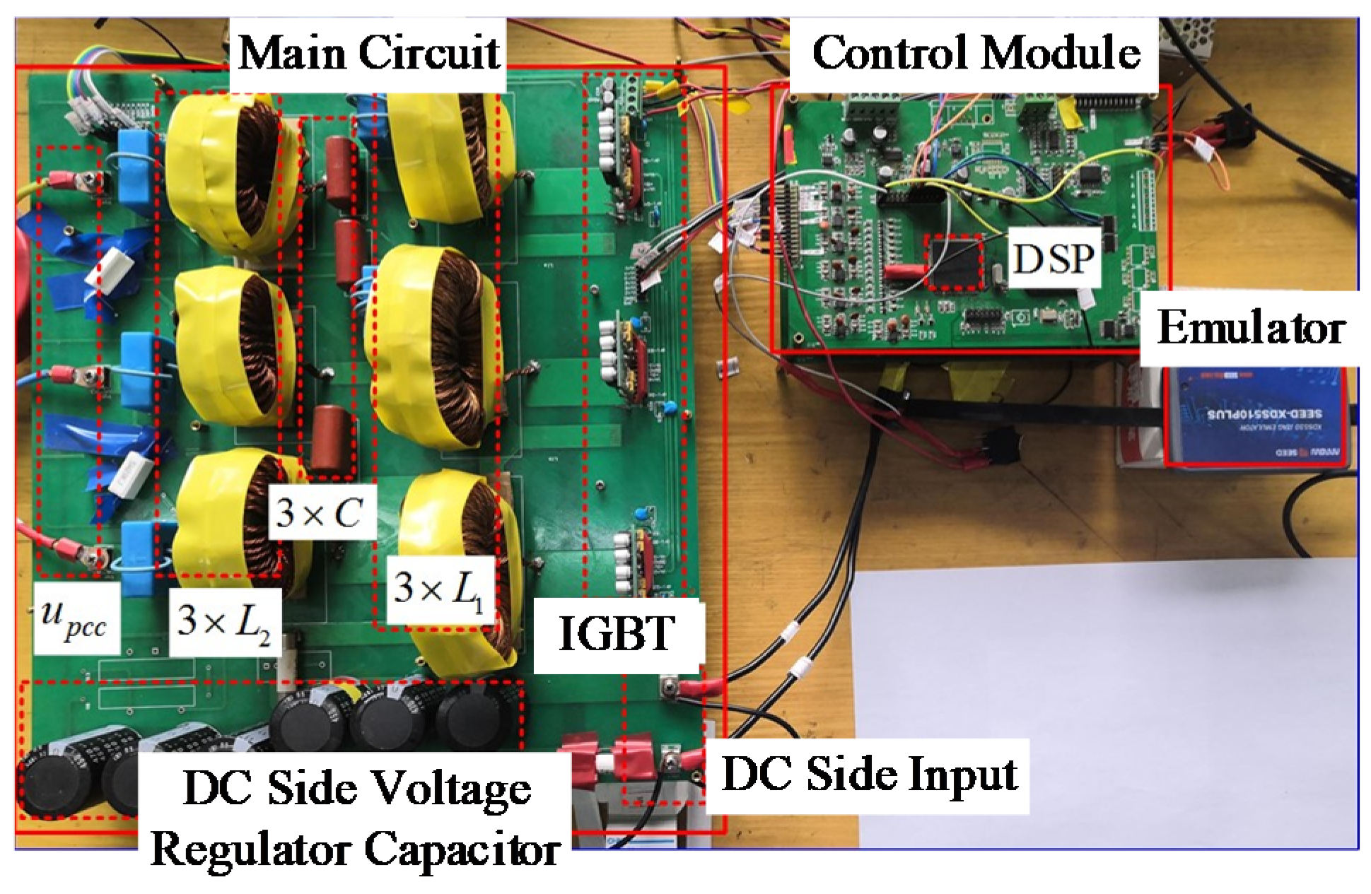
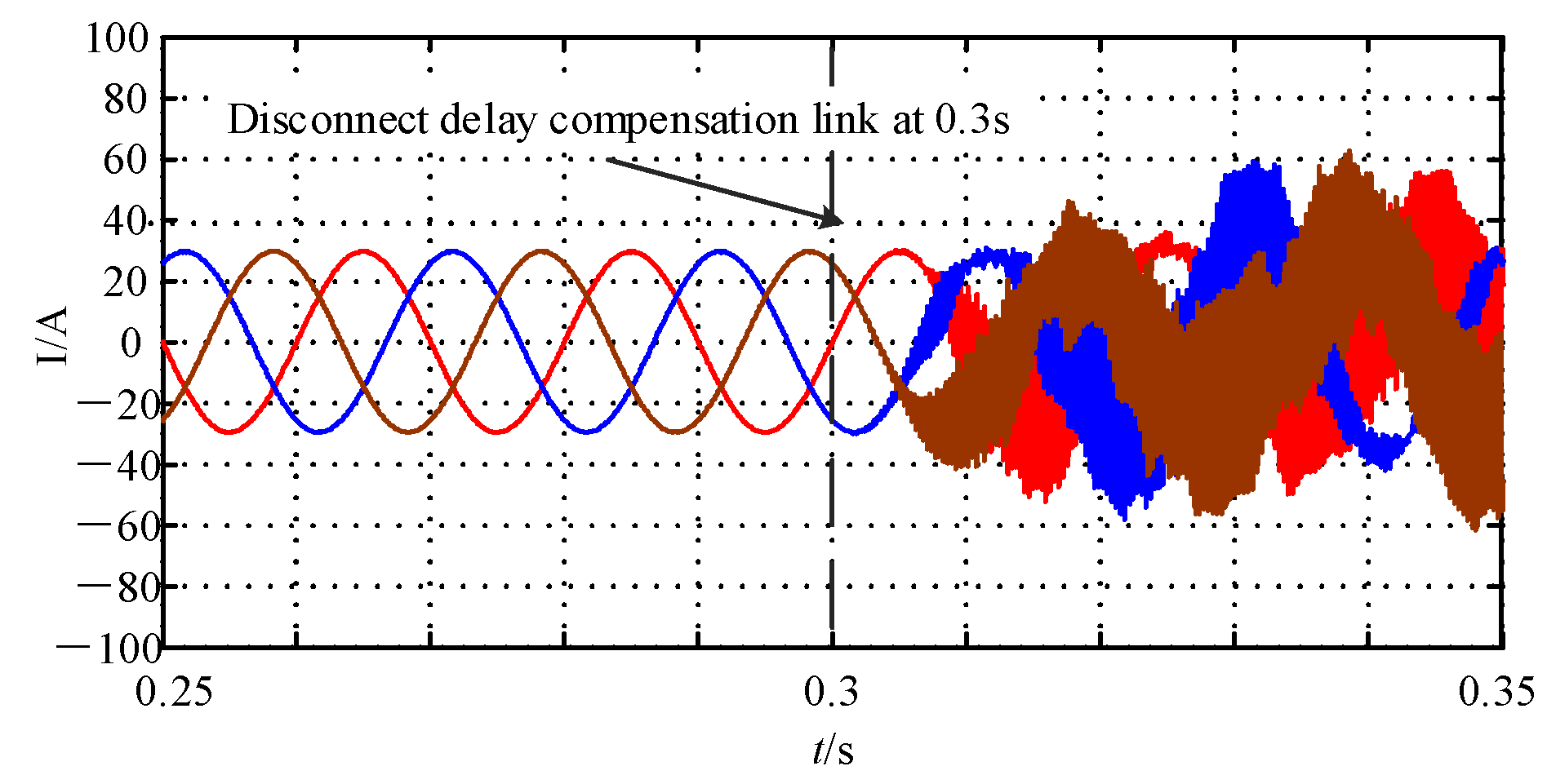
5. Simulation and Experimental Verification

In order to verify the validity of the aforementioned theoretical analysis, a three-phase LCL-type grid-connected inverter simulation platform and experimental platform were built. The specific parameters of the platform are shown in Table 2. The IGBT model used in the main circuit of this experiment is FGH40T120SMD, and the DSP control chip model used in the control circuit is TMS320F28335.
The three-phase experimental platform built is shown in Figure 9.
Figure 10 and Figure 11 are the simulation waveforms of the three-phase grid current before and after the improved delay compensation link is added under the strong power grid (power grid impedance is 0) and weak power grid (power grid impedance is 4 mH, corresponding short circuit ratio is less than 3).
Observing Figure 10 and Figure 11, it can be seen that the current into the grid becomes unstable after the off-delay compensation link in a strong power grid. This is because the active damping coefficient takes a large value, which causes the actual resonance frequency offset to be too large and exceed the effective range of active damping. When the delay compensation link is not added in the weak grid, the harmonic content of the grid current is large. This is because the steady-state margin of the inverter system at this time is low, which causes the harmonic voltage to generate a large harmonic current, which affects the quality of the grid current.
Figure 12 and Figure 13 show the experimental results of the grid current under the strong and weak grids.
It can be seen from Figure 12a that the grid current waveform becomes unstable after the delay compensation link is disconnected in a strong power grid. Figure 12b shows the phase A grid current waveform, the grid current waveform, and the PCC voltage waveform at steady state after the improved delay compensation link is added. It can be seen that the current quality at this time meets the grid access requirements, which is consistent with the simulation results.
Figure 13a shows the grid current waveform when the improved delay compensation link is not added in the weak grid, and the harmonic content is relatively large at this time. Figure 13b shows the phase A grid current waveform and the PCC point voltage waveform at steady state after the improved delay compensation link is added. It can be seen that after the improved delay compensation link is added, the output current quality of the inverter system improves, which meets the network access requirements, and is consistent with the simulation results.

6. Conclusions

The LCL grid-connected inverter system with capacitive current feedback active damping method suppresses the inherent resonance of the LCL filter while improving the harmonic filtering effect. However, the inherent delay effect in the digital control of the system reduces the effective range of the capacitive current feedback active damping method, limits the range of the active damping coefficient, and reduces the phase at the open-loop cutoff frequency. This paper has analyzed in detail the influence of each parameter of the traditional first-order lead link with a delay compensation function on the compensation effect. The infinite gain at the Nyquist frequency of the first-order lead link when the optimal coefficient is selected has the hidden danger of noise pollution.
This paper has proposed an improved delay compensation link that can achieve the optimal compensation effect while avoiding the impact on the original system amplitude. The effective range of the active damping method is expanded from (0,1/6fs) to (0,1/4fs). Finally, this paper has completed the theoretical analysis and experimental verification of the proposed method.

Author Contributions

Conceptualization, X.W. and S.W. (Shuguang Wang); methodology, X.W., S.W. (Shuguang Wang), and S.W. (Senfeng Wang); software, S.W. (Shuguang Wang), X.Z., and C.Y.; validation, S.W. (Shuguang Wang), X.W., and S.W. (Senfeng Wang); formal analysis, X.W. and S.W. (Shuguang Wang); investigation, X.W., X.Z., and C.Y.; resources, X.W. and X.Z.; data curation, X.W., S.W. (Shuguang Wang), and S.W. (Senfeng Wang); writing—original draft preparation, S.W. (Shuguang Wang) and S.W. (Senfeng Wang); writing—review and editing, X.W., S.W. (Senfeng Wang), and C.Y.; project administration, X.W.; funding acquisition, X.W. and X.Z. All authors have read and agreed to the published version of the manuscript.

Funding

This research was funded by the National Natural Science Foundation of China, grant number 52077191, 62003297.

Institutional Review Board Statement

Not applicable.

Informed Consent Statement

Not applicable.

Data Availability Statement

Not applicable.

Acknowledgments

This work is supported by Yanshan University and State Grid Hebei Electric Power Co., Ltd.

Conflicts of Interest

The authors declare no conflict of interest.

References

  1. Fang, T.; Zhang, X.; Huang, C.; He, W.; Shen, L.; Ruan, X. Control Scheme to Achieve Multiple Objectives and Superior Reliability for Input-Series-Output-Parallel LCL-Type Grid-Connected Inverter System. IEEE Trans. Ind. Electron. 2019, 67, 214–224. [Google Scholar] [CrossRef]
  2. Zhu, D.; Zhou, S.; Zou, X.; Kang, Y. Improved Design of PLL Controller for LCL-Type Grid-Connected Converter in Weak Grid. IEEE Trans. Power Electron. 2019, 35, 4715–4727. [Google Scholar] [CrossRef]
  3. Alzola, R.P.; Liserre, M.; Blaabjerg, F.; Sebastián, R.; Dannehl, J.; Fuchs, F.W. Analysis of the Passive Damping Losses in LCL-Filter-Based Grid Converters. IEEE Trans. Power Electron. 2012, 28, 2642–2646. [Google Scholar] [CrossRef] [Green Version]
  4. Pena-Alzola, R.; Liserre, M.; Blaabjerg, F.; Ordonez, M.; Kerekes, T. A Self-commissioning Notch Filter for Active Damping in a Three-Phase LCL -Filter-Based Grid-Tie Converter. IEEE Trans. Power Electron. 2014, 29, 6754–6761. [Google Scholar] [CrossRef] [Green Version]
  5. Yunhui, H.; Zefan, S.; Jinrui, T.; Binyu, X.; Sheng, H. Design and analysis of DC-link voltage stabilizer for voltage source converter as connected to weak grid. Trans. China Electrotech. Soc. 2018, 33, 185–192. [Google Scholar]
  6. Perez-Estevez, D.; Doval-Gandoy, J.; Yepes, A.G.; Lopez, O.; Baneira, F. Enhanced Resonant Current Controller for Grid-Connected Converters with LCL Filter. IEEE Trans. Power Electron. 2017, 33, 3765–3778. [Google Scholar] [CrossRef]
  7. Fang, T.; Zhang, X.; Huang, C.; He, W.; Shen, L. Control strategy to reach multiple objectives for inputseries output-parallel LCL-type grid-connected inverter system. Trans. China Electrotech. Soc. 2019, 33, 1189–1200. [Google Scholar]
  8. Fang, T.; Huang, C.; Chen, N. A phase-lead compensation strategy on enhancing robustness of LCL-type grid-tied inverters under weak grid conditions. Trans. China Electrotech. Soc. 2018, 33, 4813–4822. [Google Scholar]
  9. Sgrò, D.; Souza, S.A.; Tofoli, F.L.; Leão, R.P.S.; Sombra, A.K.R. An integrated design approach of LCL filters based on nonlinear inductors for grid-connected inverter applications. Electr. Power Syst. Res. 2020, 186, 106389. [Google Scholar] [CrossRef]
  10. Pan, D.; Ruan, X.; Wang, X.; Bao, C.; Li, W. Magnetic integration of the LCL filter in Grid-connected inverters. Proc. Chin. Soc. Electr. Eng. 2013, 33, 67–75. [Google Scholar]
  11. Xie, W.; Liu, Y.; Wang, J.; Ji, C.; Yu, J. A delay compensation method of the grid-connected inverter with LCL filter to improve robustness of the impedance shaping control. Trans. China Electrotech. Soc. 2017, 32, 178–185. [Google Scholar]
  12. He, Y.; Wang, X.; Ruan, X.; Pan, D.; Xu, X.; Liu, F. Capacitor-Current Proportional-Integral Positive Feedback Active Damping for LCL-Type Grid-Connected Inverter to Achieve High Robustness Against Grid Impedance Variation. IEEE Trans. Power Electron. 2019, 34, 12423–12436. [Google Scholar] [CrossRef]
  13. He, S.; Xiong, J.; Wang, Z.; Lin, S. Robust AD for LCL-type grid-connected inverter with capacitor current quasi-integral feedback. IET Power Electron. 2020, 13, 1332–1342. [Google Scholar] [CrossRef]
  14. Li, X.; Fang, J.; Tang, Y.; Wu, X.; Geng, Y. Capacitor-Voltage Feedforward with Full Delay Compensation to Improve Weak Grids Adaptability of LCL-Filtered Grid-Connected Converters for Distributed Generation Systems. IEEE Trans. Power Electron. 2018, 33, 749–764. [Google Scholar] [CrossRef]
  15. Semasa, M.; Kato, T.; Inoue, K. A simple and effective time delay compensation method for grid-connected inverter with an LCL filter: Application to active damping method. In Proceedings of the 2017 IEEE 18th Workshop on Control and Modeling for Power Electronics (COMPEL), Stanford, CA, USA, 9–12 July 2017; pp. 1–7. [Google Scholar]
  16. Liu, T.; Liu, Z.; Liu, J.; Tu, Y.; Liu, Z. An improved capacitor-current-feedback active damping for LCL resonance in grid-connected inverters. In Proceedings of the 2017 IEEE 3rd International Future Energy Electronics Conference and ECCE Asia (IFEEC 2017—ECCE Asia), Kaohsiung, Taiwan, 3–7 June 2017; pp. 2111–2116. [Google Scholar]
  17. Lu, M.; Wang, X.; Loh, P.C.; Blaabjerg, F.; Dragicevic, T. Graphical Evaluation of Time-Delay Compensation Techniques for Digitally Controlled Converters. IEEE Trans. Power Electron. 2018, 33, 2601–2614. [Google Scholar] [CrossRef]
  18. Chen, C.; Xiong, J.; Wan, Z.; Lei, J.; Zhang, K. A Time Delay Compensation Method Based on Area Equivalence for Active Damping of an LCL -Type Converter. IEEE Trans. Power Electron. 2017, 32, 762–772. [Google Scholar] [CrossRef]
  19. Yang, L.; Yang, J. A Robust Dual-Loop Current Control Method with a Delay-Compensation Control Link for LCL-Type Shunt Active Power Filters. IEEE Trans. Power Electron. 2018, 34, 6183–6199. [Google Scholar] [CrossRef]
  20. Wang, L.; Sun, P.; Wang, J.; Zhu, K.; Xue, T.; Zhang, Y. A Delay Compensation Method to Improve the Current Control Performance of the LCL-Type Grid-Connected Inverter. In Proceedings of the 2019 IEEE 10th International Symposium on Power Electronics for Distributed Generation Systems (PEDG), Xi’an, China, 3–6 June 2019; pp. 134–141. [Google Scholar]
  21. Liu, J.; Zhou, L.; Molinas, M. Damping region extension for digitally controlled LCL-type grid-connected inverter with capacitor-current feedback. IET Power Electron. 2018, 11, 1974–1982. [Google Scholar] [CrossRef] [Green Version]
  22. Xu, J.; Xie, S.; Zhang, B.; Qian, Q. Robust Grid Current Control With Impedance-Phase Shaping for LCL-Filtered Inverters in Weak and Distorted Grid. IEEE Trans. Power Electron. 2018, 33, 10240–10250. [Google Scholar] [CrossRef]
  23. Pan, D.; Ruan, X.; Wang, X. Direct Realization of Digital Differentiators in Discrete Domain for Active Damping of LCL -Type Grid-Connected Inverter. IEEE Trans. Power Electron. 2018, 33, 8461–8473. [Google Scholar] [CrossRef] [Green Version]
Figure 1. Topology and control structure of three-phase LCL-type grid-connected inverter.
Energies 14 02730 g001
Figure 2. Block diagram of grid-connected inverter under digital control.
Energies 14 02730 g002
Figure 3. Comparison of transfer function Bode diagrams with different active damping coefficients: (a) considering the digital delay; (b) without considering the digital delay.
Energies 14 02730 g003
Figure 4. Structure of zero-gain first-order lead link.
Energies 14 02730 g004
Figure 5. Bode diagrams of first-order lead link under different coefficient changes: (a) Bode diagrams of first-order leading links under different values of m; (b) Bode diagrams of first-order leading links under different values of n; (c) Bode diagrams of first-order leading links under different values of k.
Energies 14 02730 g005
Figure 6. Comparison of new delay compensation function with first-order lead link.
Energies 14 02730 g006
Figure 7. Insertion position of delay compensation function.
Energies 14 02730 g007
Figure 8. Range of active damping with different coefficients.
Energies 14 02730 g008
Figure 9. Three-phase LCL grid-connected inverter experimental prototypes.
Energies 14 02730 g009
Figure 10. Switching of delay compensation link in strong grid.
Energies 14 02730 g010
Figure 11. Switching of delay compensation link in weak grid.
Energies 14 02730 g011
Figure 12. Experimental results under strong grid: (a) switching of delay compensation links; (b) network current and PCC voltage at steady state.
Energies 14 02730 g012
Figure 13. Experimental results under weak grid: (a) the grid current waveform when no delay compensation link is added; (b) network current and PCC voltage when delay compensation link is added.
Energies 14 02730 g013
Table 1. Effect of digital delay in different frequency ranges.
Frequency Range(0, 1/6fs)(1/6fs, 1/3fs)(1/3fs, 1/2fs)
cos(1.5ωTs)positivenegativenegative
sin(1.5ωTs)positivepositivenegative
Table 2. System parameters.
ParameterSymbolValue
DC voltageUDC500 V
Inverter side filter inductanceL12 mH
Filter capacitorC9.4 μF
Grid-side filter inductanceL20.4 mH
Output active powerPo4950 W
Phase voltage amplitudeug110 V
Switching/sampling frequencyfs20 kHz
Compensation coefficientn1
Active damping coefficientHi0.04
Current loop proportional coefficientKP0.023
Current loop integral coefficientKI65.5
Publisher’s Note: MDPI stays neutral with regard to jurisdictional claims in published maps and institutional affiliations.

