1. Introduction
In recent years, the diffusion of renewable sources has implied a wide use of power converters for interfacing them to the grid. While innovative topologies of converters have been proposed, the conventional configurations have been widely adopted in commercial devices. For several applications, when the source voltage has to be increased to match the grid voltage, such as photovoltaic (PV) systems, integration of storage systems, fuel cells and so on, the most used topology is the DC/DC boost converter because of its simplicity of control and low cost. The typical topology used to interface DC renewable sources and storages to the grid is made up of a boost converter and a voltage source inverter connected to the AC mains by means of inductive filters [
1,
2,
3]. In most of the plants, if insulation between DC and AC side is required, a transformer is interposed. This transformer, if properly designed, can operate also as a filter for the inverter. Control of the boost converter has usually two main goals: (i) increasing the output voltage of the source to adapt it to the grid voltage; (ii) implementing a control algorithm, such as a MPPT, to optimize the energy transfer of the source or of the storage.
In several applications it is not possible to use a single boost converter because of the high ratio between input and output voltages or because of the necessity of coupling different sources with different control algorithms. For this reason, several architectures based on the series or parallel connection of boost converters have been proposed [
4,
5]. For a proper operation, it would be useful to accurately know which is the output characteristic of the boost converter when it implements a control algorithm on a variable voltage source. Therefore, a model of boost converter capable of predicting the output voltage and current in any operating condition could be beneficial.
The extensive research about modelling of boost converters started at the beginning of the 1980s. The conventional model takes into account the switching of the power electronic devices, but it does not consider the losses that are unavoidable in practical implementations. The first models of the ideal boost converter have been presented in [
6,
7] and are now reported in all the books about power electronics (see for example [
8]). The first efforts for modelling the parasitic effects date back to the beginning of the 1990s. In [
9], the electrical model of the boost converter including the parasitic resistances of inductors and capacitors as well as the voltage drop and conduction losses of the switch and the diode is proposed. Other models taking into account parasitic resistances and non-linear conduction losses have been presented in more recent years [
10,
11]. In these models, anyway, the switching losses are not included.
Some more sophisticated models capable of taking into account also the switching losses, both for hard switching and soft switching converters, have been presented in [
12,
13,
14]. However, these models evaluate the global switching losses of the converter, thus allowing us to predict its efficiency, but they are not able to estimate their impact on the voltage-current curves. Some attempts were made to include switching losses in
output impedance models [
15]. Even if these models allow us to take into account the switching losses in the response of the converter, they do not show the effect of these losses on the equivalent duty cycle of the converter. For this reason, they cannot be used easily for control purposes. As mentioned above, a model that also considers the effect of the losses on the input-output characteristics could be very useful to understanding the actual performances of multiple boost converters with series- or parallel-connected outputs, improving the controllability of these converters. Moreover, the effective impact of switching losses on output voltage-current characteristic of the converter would be very interesting in wireless sensor applications where the overall available power is very low [
16]. The analytical calculation of the effective duty cycle considering switching losses is proposed in [
17] for boost converters. Nevertheless, the proposed model neglects the effect of the switching transient on the output current. In practice, it considers that the integral of the current on the switching device is not affected by the switching transient. This is true only if the rise time and the fall time of the component are equal. In this hypothesis, the duty cycle is still equal to the ratio between output and input current but not between output and input voltage. Unfortunately, at present, there are no models in the literature that are capable of taking into account the effect of the switching transient on both output voltage and current considering different rise and fall times of the switching components. In [
18], a steady-state model useful for load flow calculations is proposed, but it cannot be employed for dynamic simulations. Finally, in [
19], a Hammerstein model is presented. Its results are accurate, but its formulation is so far from the physical circuit that the results are not portable to other configurations. As clearly analyzed in [
20], averaged models can be very useful for stability analysis of power converters. Anyway, at present, no average models capable of taking into account the effect of switching losses on both output voltage and current have been proposed. In this paper, a new average model taking into account switching losses will be presented for a boost converter, but the proposed approach can be easily extended to all the DC–DC converters. It is worth noting that this is the first time that an average model of a power converter including switching losses and considering different rise and fall times of the switching components, is proposed.
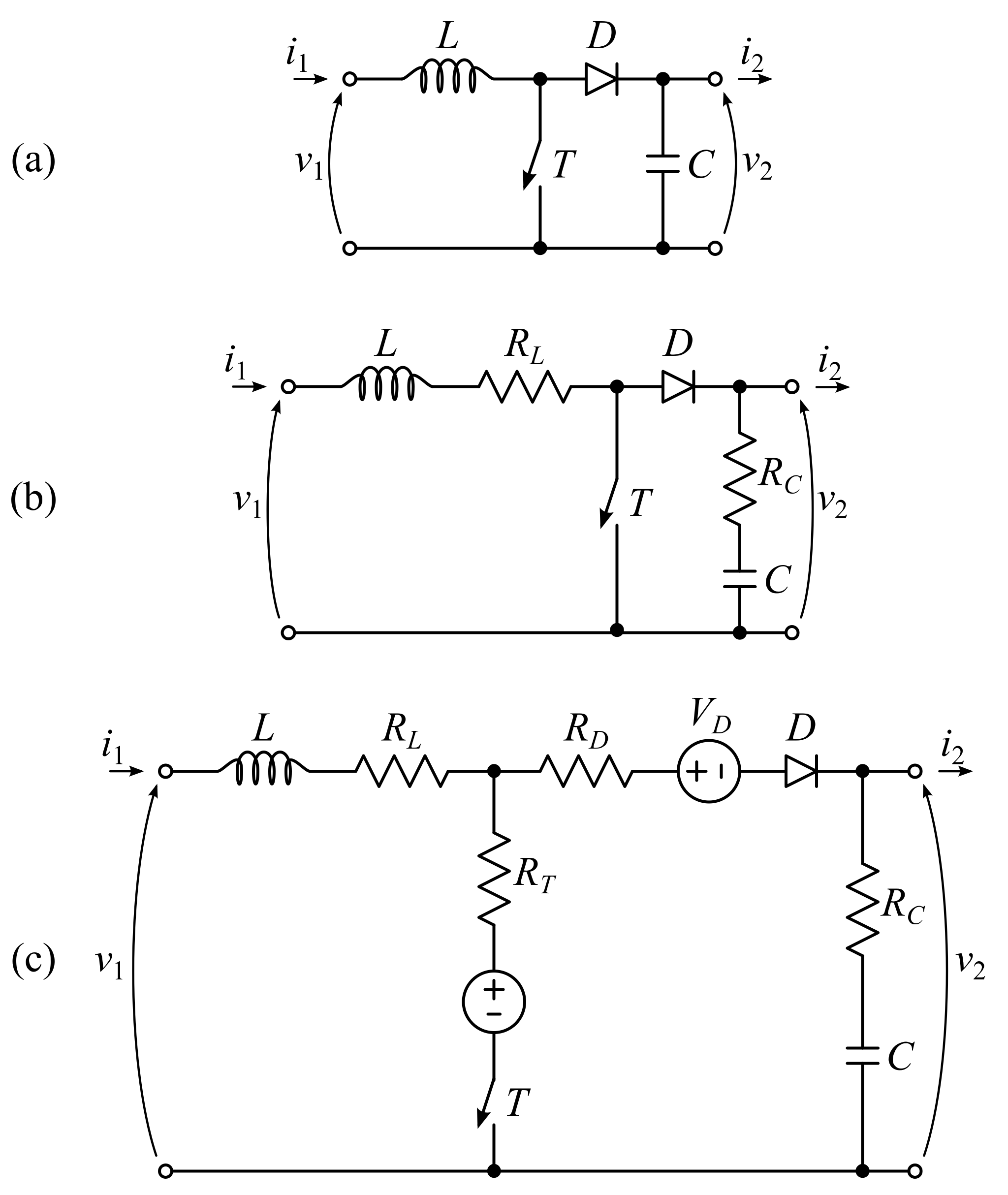
Nowadays, there are basically three traditional boost converter models proposed in the literature:
The conventional model of the ideal converter, losses are neglected (
Figure 1a);
The model considering only the parasitic elements of the inductor and the capacitor (
Figure 1b);
The model that includes the parasitic elements of both the reactive components and the semiconductors (
Figure 1c).
This paper proposes a new electrical equivalent model capable of taking into account also the switching losses and to calculate their effect on the output voltage-current characteristic. This model, based only on standard circuit elements, allows the calculation of output voltage and current separately and it can be used for steady-state and dynamic simulations, as long as the converter response to the control signal (e.g., variation of the duty cycle) can be considered as instantaneous. The main contribution of this paper is distinguishing between the duty cycle of the PWM signal driving the switch from the equivalent duty cycles of the voltage and current waveforms, which are affected by the non-ideal switching transients. By taking this effect into consideration, the average model of conventional DC/DC converters (not just limited to boost converters) can more accurately represent the actual output voltage-current characteristics.
The case study of a boost converter has been considered in this paper as a case study, but in principle the proposed approach can be applied to all DC–DC converters. In
Section 2, the model equations of the considered converter have been derived while in
Section 3 the proposed model is discussed. In
Section 4 the experimental setup used for the validation tests is described.
Section 5 reports the experimental validation in several operating conditions is reported, as well as a comparison with the results obtained by using the conventional models.
2. Boost Converter Modeling
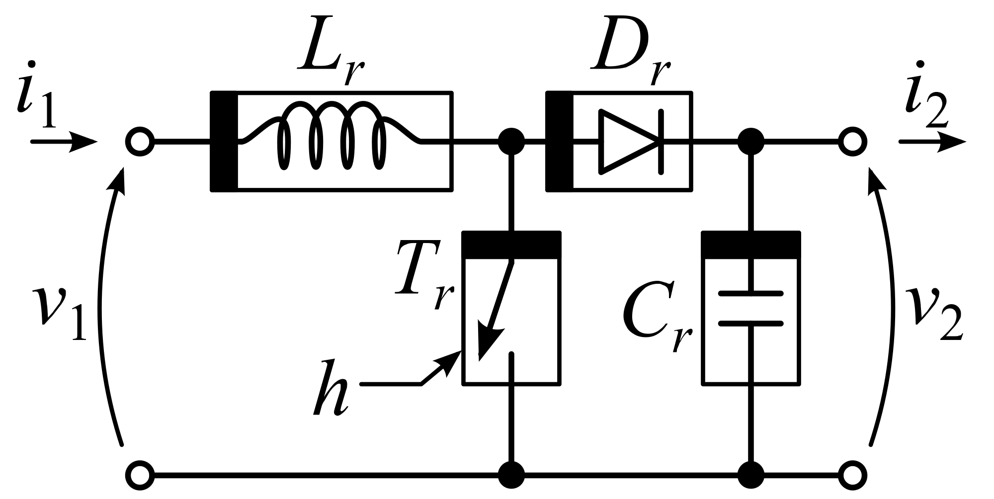
Figure 2 shows the generic equivalent network of a boost converter [
17,
21]. It is made up with the following components: an inductor
Lr, a switch
Tr, a diode
Dr and a capacitor
Cr. According to the models that are adopted to represent their behaviors, the equivalent circuit shown in
Figure 1 and described in the previous section could be obtained. The gate signal applied to the electronic switch
Tr is modeled with the corresponding discrete-valued switching function
h [
21] (
h = 1 when
T is ON and
h = 0 when
T is OFF).
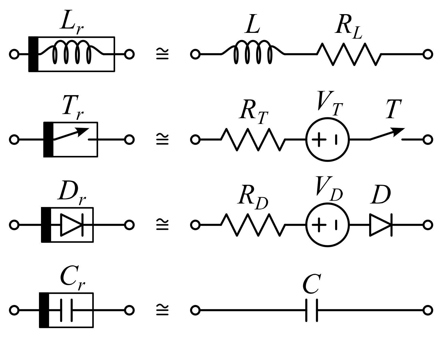
An accurate modeling of the boost converter requires properly considering the non-idealities, which means adopting adequate equivalent circuit representation for
Lr,
Cr,
Dr and
Tr First of all, the winding of an actual inductor has finite resistance, thus causing non-negligible Joule effect loss. Therefore, the physical inductor
Lr can be modeled with the series connection of an ideal inductor
L and an ideal resistor
RL (
Figure 3).
The switching element
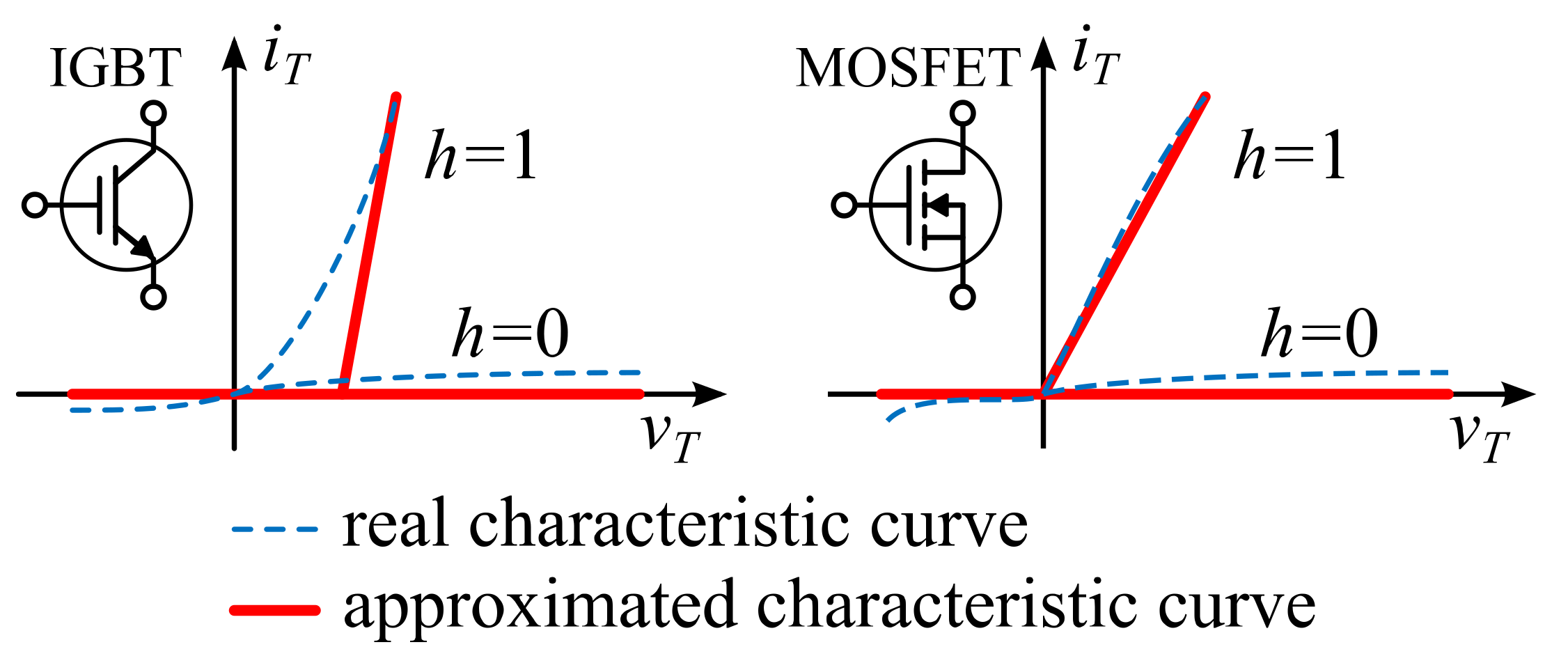
Tr of the power converter is typically a MOSFET or IGBT. Despite their working principles are significantly different, their electrical behaviors can be represented by using the same circuit model. As usual, the losses of both devices can be categorized in two classes: conduction losses and switching losses [
8]. The first are due to the fact that when the transistor is switched on, its voltage drop is small but not null [
8,
22], according to the blue dashed characteristics plotted in
Figure 4.
Figure 4 also reports the approximated characteristics of the considered electronic switches. They are widely employed since they can be modeled as the series connection of an ideal switch
T, an ideal voltage source
VT and an ideal resistor
RT (
Figure 3).
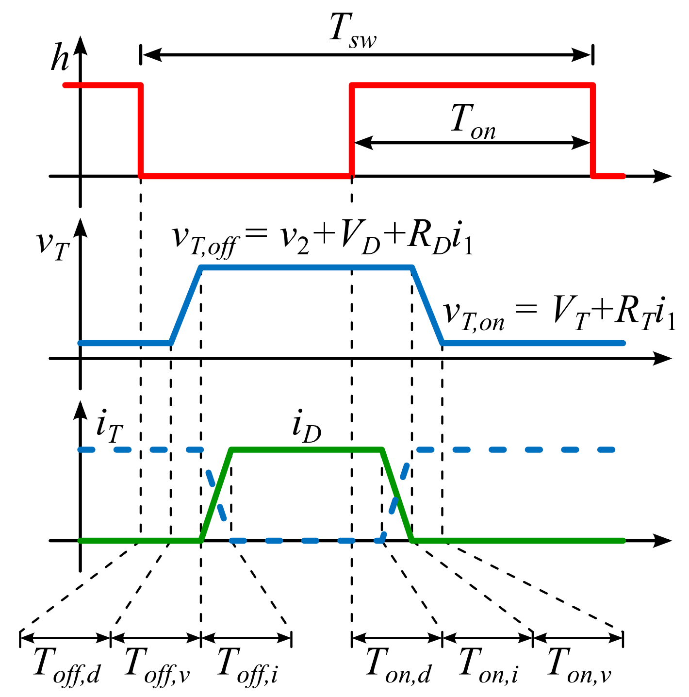
The second type of loss is due to the high-frequency commutation of the electronic switches. The transition from the OFF-state to the ON-state, and vice versa, produces voltage and current transients that cause energy losses. In particular, during these switching transients, current and voltage waveforms in both MOSFETs and IGBTs can be modeled as in
Figure 5 [
22,
23]. It can be noted that there are time frames in which both the voltage
vT and current
iT are not zero, thus causing finite power losses.
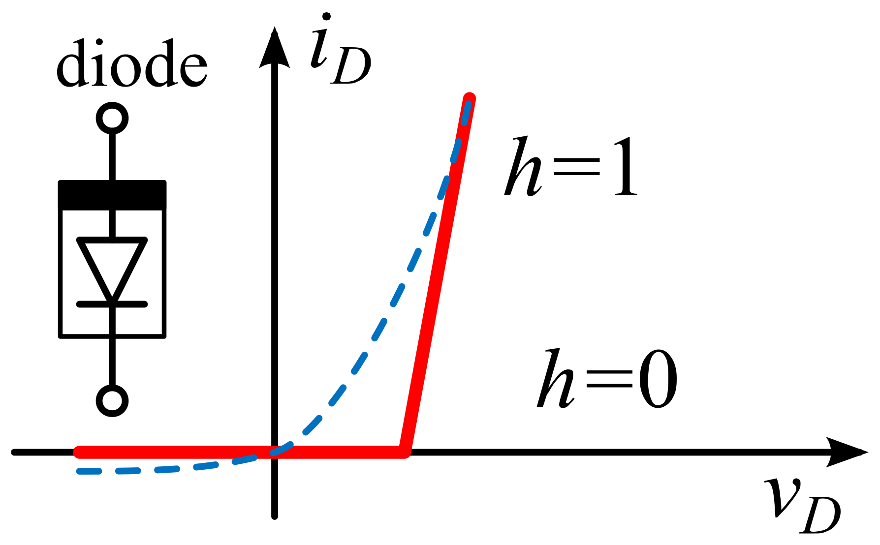
In general, even the diodes are affected by conduction and switching losses. However, in this case the switching losses can be considering as negligible when compared to the conduction losses. The volt-ampere curve of a typical diode is shown in
Figure 6. It can be noted that it is pretty similar to the ON-state
v-i curve of an IGBT, therefore it can be approximated by using a circuit model made of the series connection between an ideal diode
D, an ideal resistor
RD and an ideal voltage source
VD, as depicted in
Figure 3.
The last element of the power converter to be modeled is the output capacitor. The losses due to the non-ideal behavior of this element are generally some orders of magnitude lower than those due to the other components, so they can be neglected without sacrificing the model accuracy (
Figure 3).
If we suppose that the switching losses are negligible, the behavior of the boost converter is described by the well-known circuit reported in
Figure 1a. Introducing the controlled voltage and current sources
vT and
iD, it can be redrawn as in
Figure 7.
Having introduced:
where
is the average output voltage,
VT and
RT are the parameters of the linearized current-voltage characteristic of the electronic switch (
Figure 3), while
VD and
RD are the parameters of the linearized current-voltage characteristic of the diode (
Figure 3). Therefore, the effect of conduction losses occurring in the semiconductors can be considered by properly adjusting the controlled voltage source.
When switching losses cannot be neglected, typically this circuit is still employed but the switching losses are calculated separately [
1]. However, although this approach is rather accurate in predicting the energy efficiency of the power electronics converter, it is not able to faithfully represent the relations between voltages and currents.
Switching losses arise from the fact that, during the turn-off transient, the current in the electronic switch is not nil when the voltage starts to build up. Similarly, the current in the electronic switch starts to grow before the voltage begins to decrease during turn-on. Assuming that the current and voltage of the electronic switch changes linearly during turn-on and turn-off transients, the simplified waveforms shown in
Figure 7 can be considered.
A possible approach to include the switching losses in the model depicted in
Figure 6 is properly adjusting the controlled voltage and current sources
vT and
iD according to the waveforms depicted in
Figure 7: this represents a key aspect in obtaining the proposed model of DC/DC converter. Once the sources
vT and
iD have been properly set, the state-space representation can easily be deduced from the equivalent circuit of the converter. The following second order system can be written as:
3. Proposed Model
The dynamic behavior of the boost converter is extremely fast so that, for many applications, its response to a variation of the duty cycle can be considered as instantaneous. Let us suppose continuous conduction mode operation; as usual, it is supposed that the electrical quantities are composed by two spectrally separated terms: a low frequency component and a high frequency ripple. In a properly sized converter, the ripple of the state variables is typically considerably smaller than their low-frequency content during typical operation. Therefore, according to the previous assumptions, the switch-mode converter can be modeled by using algebraic relationships between the average (ripple-free) voltages and currents, which can be computed by equating to zero the derivatives of the state-space system (4):
where
and
are the average input voltage and current,
is average output current,
and
are the average switch voltage and diode current, respectively. Considering the approximated waveforms during the turn-on and turn-off transients reported in
Figure 7, it becomes clear that both
and
are affected by the duration of the turn-on and turn-off transients. In particular, their values can be expressed as follows:
where
δ =
Ton/
Toff is the usual duty cycle of the boost converter, which can be seen as the low-frequency content of the switching function
h, while:
From a physical point of view,
δV represents the equivalent variation of the duty cycle corresponding to the change of the average voltage across the electronic switch due to the switching transients and
δI represents the equivalent variation of the duty cycle corresponding to the change of the average current flowing through the diode due to the commutations. Under ideal conditions, both
δV and
δI are zero, thus (6) boils down to the classical model of the boost converter. Substituting (6) in (5) allows obtaining the output current and voltage, which are given by:
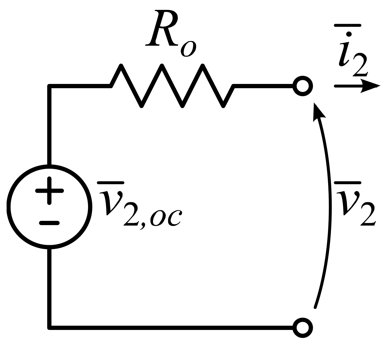
Then, substituting (9) into (8) allows obtaining the output voltage as a function of the secondary current and duty cycle; it can be written as:
where
and
Ro are the open circuit voltage and the output resistance of the converter, respectively, leading to the equivalent circuit reported in
Figure 8. Their expressions are:
It is worth noting that losses result in a finite output resistance Ro of the converter, thus its output voltage becomes more load dependent. As expected, is strictly related to , but it is worth noting that being its value increases by switching losses.
When the boost converter is coupled with renewable sources or storages, the duty cycle
δ is chosen by the control algorithm, so that both the input current and voltage are imposed by the controller and by the volt-ampere characteristic of the source. Furthermore, the average output voltage and currents are mutually dependent, according to the load connected to the converter. For this reason, it is particularly useful to compute the expression of the average output current (or voltage) as function of the inputs and of the duty cycle. After some computations, the average output voltage results:
having introduced
δP, namely the equivalent variation of the duty cycle due to the switching transients:
Looking at the expression (13), δP is half of the time spent during commutation referred to the switching period.
Alternatively, the expression of the average output current can be obtained:
The total output power can be calculated by combining (8) and (9). Obtaining from (9) the expression of
while multiplying it by
allows computing the output power
P2 as a function of the input quantities and of the duty cycle
δ. It finally results as follows:
having introduced the input power
. In practical applications, the duration of the switching transients must be significantly lower with respect to the total duration of the switching period. In this respect, assuming that
δV <<
δ,
δV << 1 −
δ and
δI << 1 −
δ, thus excluding extreme boost ratios (15) can be simplified noticeably; furthermore, the switching losses
Psw can be separated from conduction losses
Pcond:
where:
The achieved formulation can be particularly useful for the design of power converters, since it highlights the main contributions of each component to conduction and switching losses. In particular, let us look at (17). Concerning conduction losses, it can be noticed that an important energy contribution is provided by the inductor parasitic resistance, in which the input current i1 is continuously flowing, whatever the operating condition of the power converter. On the contrary, the transistor and diode conduction losses are affected by the duty cycle and this can easily be explained by observing that:
For small values of δ, the current i1 flows through the diode for a long fraction of the switching period and, consequently, low drop is key when the converter is aimed for working mainly at low boost rates.
For large values of δ, instead, transistor conduction losses become relevant as i1 primarily flows through it. In order to optimize efficiency at high boost rates, the voltage across the electronic switch should be reduced.
Finally, from the analysis of (17), it can be noticed that that switching losses are primarily affected by the input power (P1) and by the duty cycle. In particular, the model states that for large values of δ, Psw increases dramatically. For this reason, when high voltage boost rates are requested, it is important to optimize the selection of a proper electronic switch and gate driver in order to minimize the duration of turn-on/off transients.
4. Experimental Setup and Preliminary Measurements
In order to validate the proposed model, an experimental setup has been developed. A boost power converter made up of the following components has been considered:
470 μH inductor Murata® Power Solutions, 4A max. DC current;
Power MOSFET IXYS® IXFH40N30 driven by Microchip® TC1413N driver;
Schottky diode ON Semiconductor® MBRF20100CT;
2 × 220 μF series-connected electrolytic capacitors.
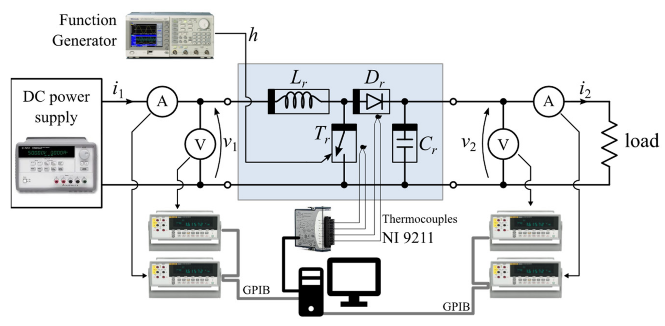
The model requires the knowledge of some characteristic parameters of the components that, as well known, may exhibit a non-negligible temperature dependency, especially those related with the semiconductors. For this reason, the parameters have been estimated under steady-state thermal conditions, considering a reference case temperature of 40 °C for both the diode and the electronic switch. The case temperature of the components has been monitored by means of K-type thermocouples and controlled by adjusting switching frequency and duty cycle. The operating conditions have been properly changed just before the estimation of the parameters; since the measurement time is fast with respect to the thermal dynamics, the temperature of the semiconductor devices can be considered virtually constant. The input port of the converter has been connected to an Agilent E3634A DC Power Supply applying a voltage
V1 = 20 V; 4 A current limit has also been set according to the maximum current of the inductor. A fixed resistor having a resistance value
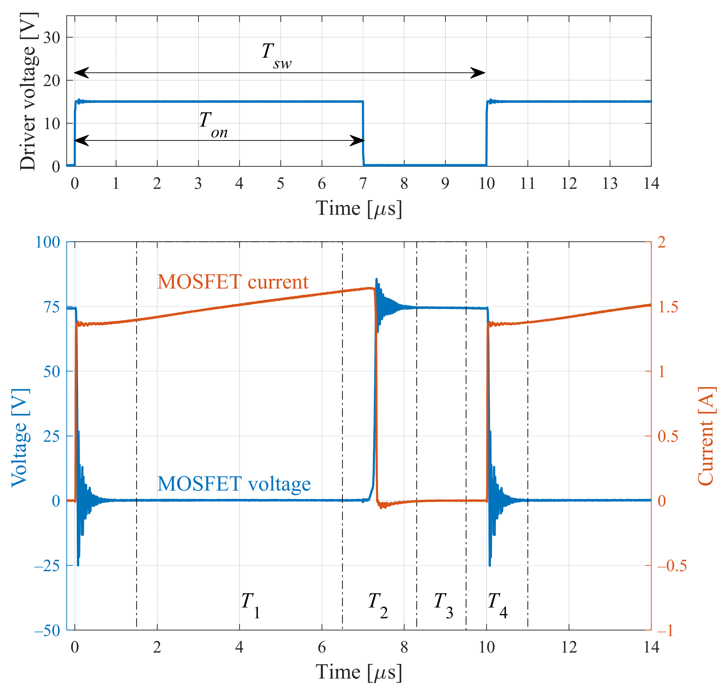
R = 170 Ω has been connected to the output port. The MOSFET driver has been connected to a Tektronix AFG 3022B function generator providing the PWM signal. Voltage and current waveforms (
Figure 9 reports those related to the MOSFET) have been acquired by means of a wide bandwidth digital oscilloscope and a closed-loop Hall effect current probe. For each quantity (acquired for 40 °C case temperature), four segments of the sampled waveforms have been extracted and processed for computing the model parameters, in particular:
MOSFET conduction phase (T1);
MOSFET turn-off transient (T2);
Diode conduction phase (T3);
MOSFET turn-on transient (T4).
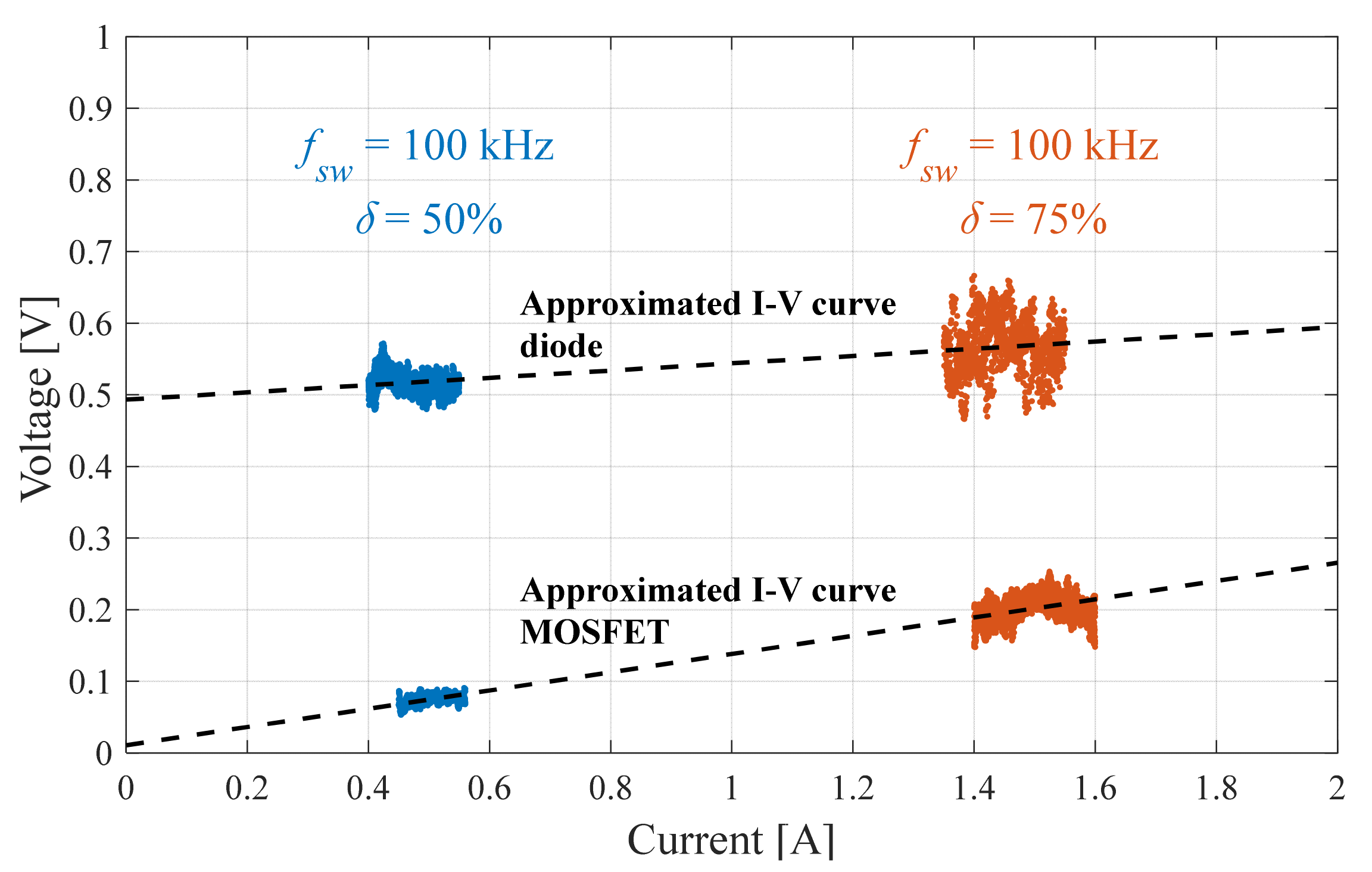
The segments
T1 and
T3 of the signals have been extracted for two duty cycle values (50% and 75%) and used for identifying the on-state models of the MOSFET and diode during conduction (according to
Figure 5).
Figure 10 reports the acquired voltage and current samples related to these waveform parts, together with those approximated on the state curves, whose parameters (
VT,
RT,
VD and
RD) have been estimated by means of the ordinary least squares method.
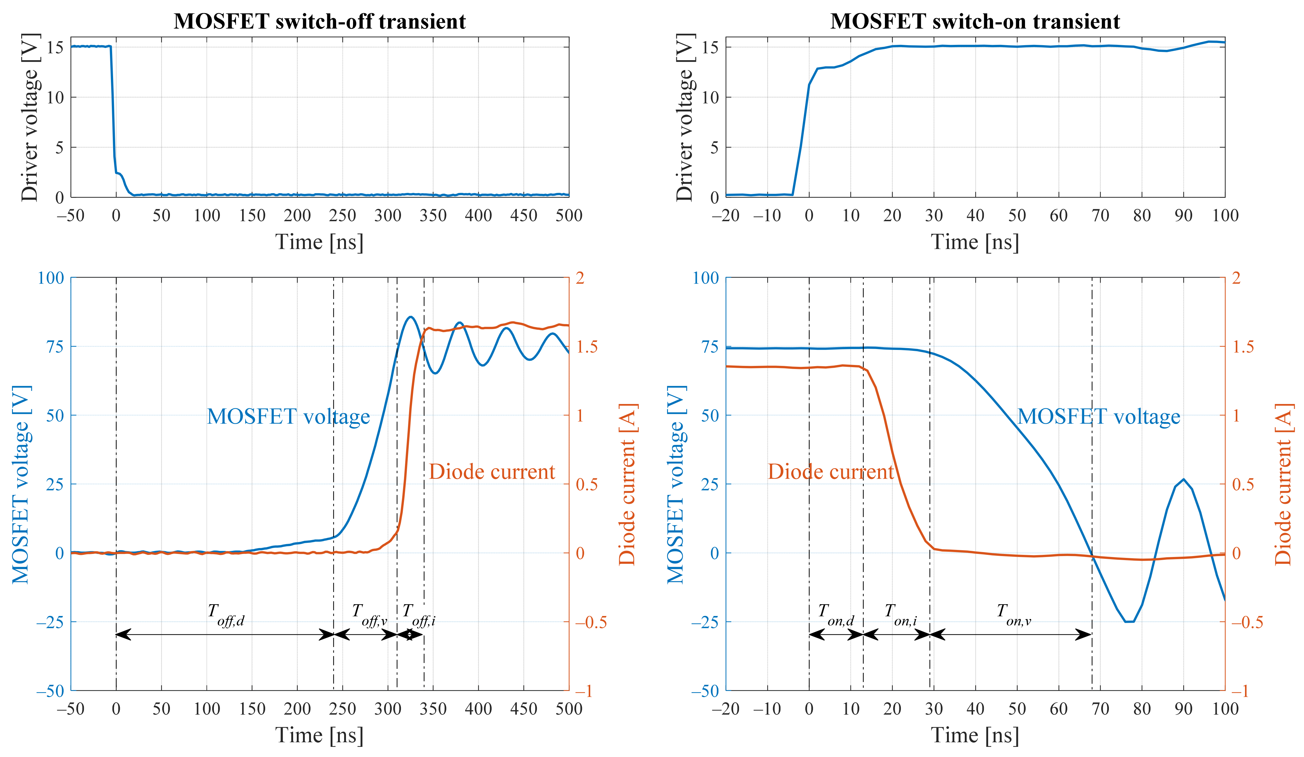
Concerning the MOSFET switch-off/on transients, their durations have been measured by observing the voltage and current waveforms within the time intervals
T2 and
T4 respectively (as reported in
Figure 11). The same procedure has been repeated for different duty cycles and similar delay times have been observed.
Thanks to these experiments, the parameters have been successfully extracted and reported in
Table 1. As discussed in
Section 2, another relevant parasitic element is represented by the series resistance of the inductor, which has been measured by means of a 6½ digit multimeter (Fluke 8845A) in four-wire configuration.
Even considering the time-consuming procedure for identifying the model parameters, which is meant for the validation of the power electronic components model, the proposed formulation can still praise practical applications especially within the design stage of DC–DC converters. Indeed, all the model parameters can be easily obtained from the technical datasheets of the power converter components, without the need for performing dedicated experiments:
The v-i curves of electronic switches and diodes is commonly reported in a direct way, often together with its temperature sensitivity. A linear approximation, when not present, can be easily obtained.
The switch on/off delays adopted by the model are not commonly listed with the required level of detail. Nevertheless, they can be deduced easily from the typology of the MOSFET driving circuit and the gate charge characteristic curve (normally found in technical datasheets) using the expressions proposed by [
24].
Table 1 also lists the model parameters reported or deduced from the datasheets of the components. It can be noted that their values are generally similar to the measurements and the main differences can be reasonably attributed to their temperature dependency, manufacturing tolerances, and other source of uncertainty. This result, other than validating the characterization, strengthen the exploitability of the proposed DC–DC converter model. In addition, if the datasheet provides information about the spread of some parameters, it is possible to analyse the impact of manufacturing tolerances on the operation of the converter.
After the characterization procedure, the aforementioned power converter was tested for 16 values of duty cycle
δ (from 0.05 to 0.80) and seven different switching frequencies
fsw = 1/
Tsw (from 50 kHz to 200 kHz). Input and output average voltages and currents were measured by means of four GPIB-controlled Fluke 8845A multimeters. The case temperatures of the semiconductor devices were acquired by using K-type thermocouples and a National Instruments
® NI 9211 thermocouple input module connected to the PC. The tests were carried out considering a case temperature of 40 °C, which was controlled with the same method employed during the preliminary parameter estimation.
Figure 12 reports the diagram of the experimental setup.
5. Experimental Results
The measurement results obtained with the experimental setup described in the previous section were compared with those predicted by three models of the boost converter:
Model 1: proposed model, considering the series resistance of the inductor as well as conduction and switching losses occurring in the semiconductor devices.
Model 2: conventional model considering the series resistance of the inductor and the conduction losses in the semiconductor devices.
Model 3: ideal (lossless) boost DC/DC converter.
The aforementioned models can be employed to predict the output voltage and current for a known input voltage, input current, and duty cycle for different switching frequencies. For the proposed model (Model 1), this means introducing the measured average input current and voltage, together with duty cycle and switching frequency, in (8) and (9). The expression of the predicted voltage and current according to Model 2 can be also obtained from (8) and (9) by assuming δV = δI = 0. The equations of the ideal boost converter (Model 3) correspond to (8) and (9), once having set to zero all the parasitic parameters.
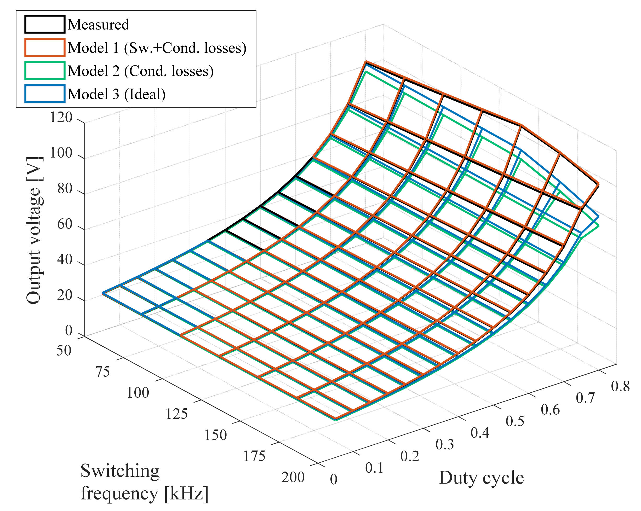
Figure 13 compares the predicted output voltage using models 1, 2 and 3 with the experimental results. The output voltage decreases at the higher switching frequencies (
fsw ≥ 150 kHz) when
δ = 0.8; the reason is that the 4 A input current limit is reached, and this leads to a reduction of the input voltage. It can easily be noticed that Model 1 is by far the most accurate, especially at high duty cycles and switching frequencies, thus when the finite duration of the switching transients has the highest impact. It should be noted that actually the duration of the turn-on and turn-off transients depends on the operating conditions of the electronic switch, in particular on the drain-to-source voltage. Even if it has not been considered in the proposed model, the resulting accuracy is still remarkable. Model 2, which includes the conduction losses, shows higher errors than Model 3 in predicting the output voltage. This means that the model of the ideal converter provides a better prediction of the output voltage with respect to the model that includes conduction losses. This may appear strange at a first sight, but actually the output voltage results from a partial compensation between non-idealities (conduction and switching loss) that, for given operating conditions, produce opposite effects. Reminding ourselves of (8), the presence of conduction losses decreases the expected output voltage for given input current, voltage and duty cycle. By contrast, when the switching transients are considered (hence
δV > 0), the delays results in an increase of the output voltage with respect to ideal switching. Therefore, it may be that considering conduction losses but instantaneous switching produces a worse predicted output voltage with respect to that obtained with the ideal converter. From
Figure 13, it becomes evident that Model 3 still underestimates the output voltage; this means that, in this respect, the impact of non-ideal switching is stronger with respect to that due to conduction losses, especially at the highest switching frequency.
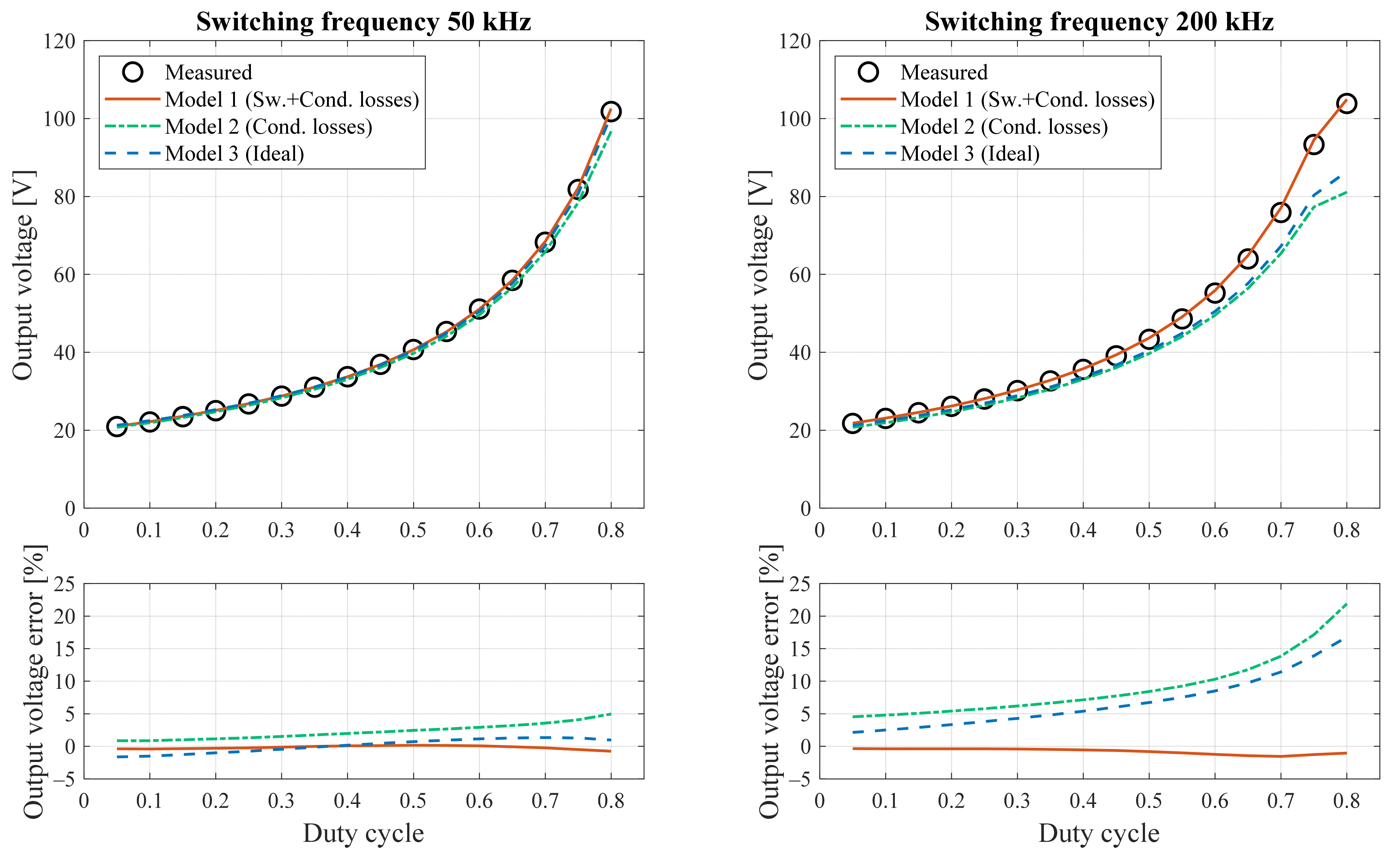
Figure 14 reports the results obtained at the lowest and the highest switching frequencies, 50 kHz and 200 kHz, respectively. When
fsw = 50 kHz is considered, the matching between the different models is quite good, but the proposed model features a much lower maximum error of less than 0.8% with respect to Model 2 (almost 5%) and Model 3 (1.6%). As expected, the maximum errors for Model 2 and Model 3 increases with the switching frequency, being 22% and 17%, respectively, when
fsw = 200 kHz. Model 1 remains fairly accurate, since the maximum error does not exceed 1.6%. It is worth noting that some hundreds of kHz is a frequency more and more used in new power converters. Indeed, diffusion of SiC and GaN components pushed the frequency to very high values (up to 1 MHz) even for power converters [
25].
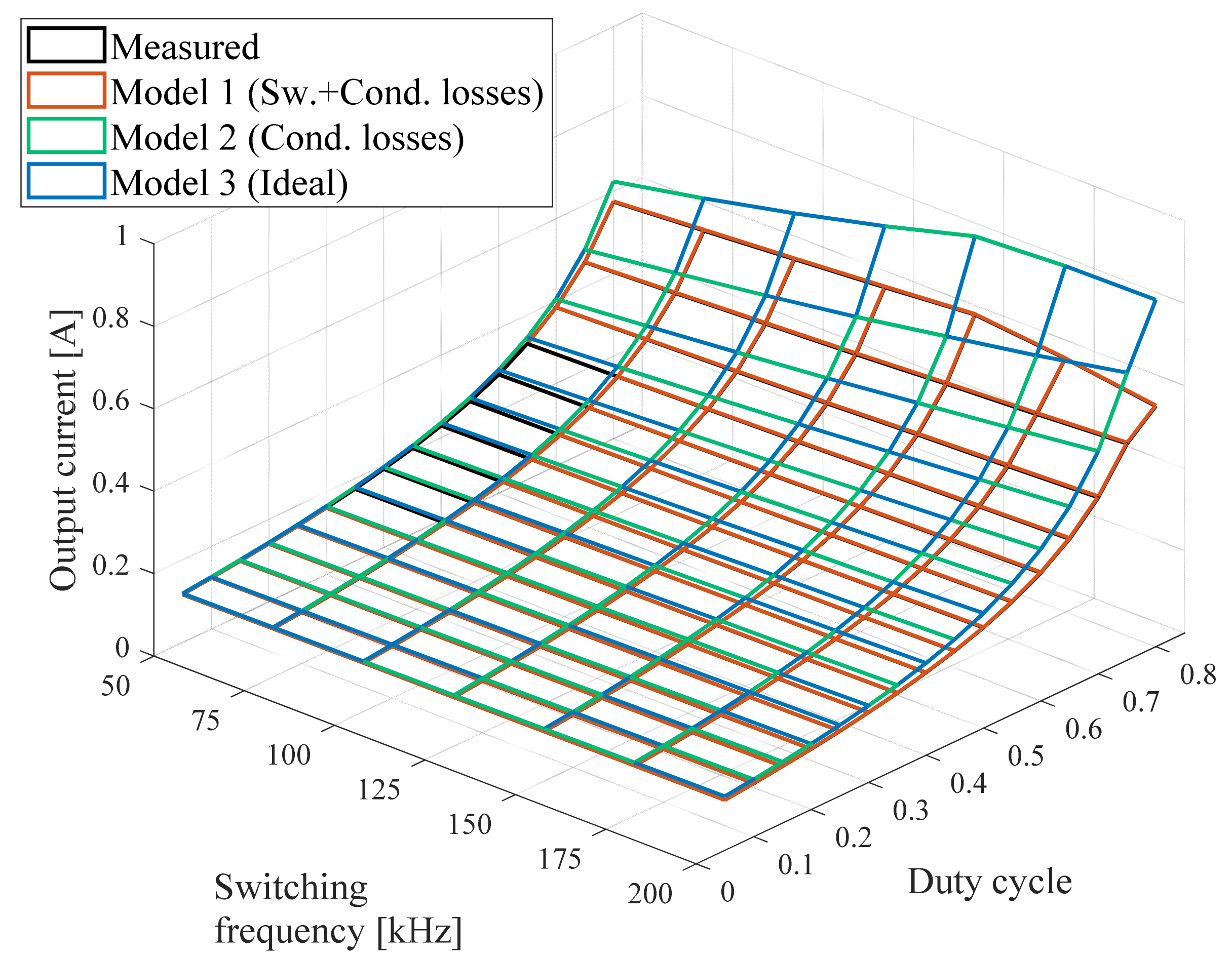
Figure 15 reports the measured and estimated output current using the three models. In this case, the results of Model 2 and Model 3 overlaps, since (9) does not contain parameters related to conduction losses. The output current is clamped because of the aforementioned 4 A input current limit. It can be noticed that the prediction of Model 1 is still much closer to the experimental results. Neglecting the switching transients leads to an overestimation of the output current, as shown by (9).
The errors of Model 2 and Model 3 increases with the switching frequency.
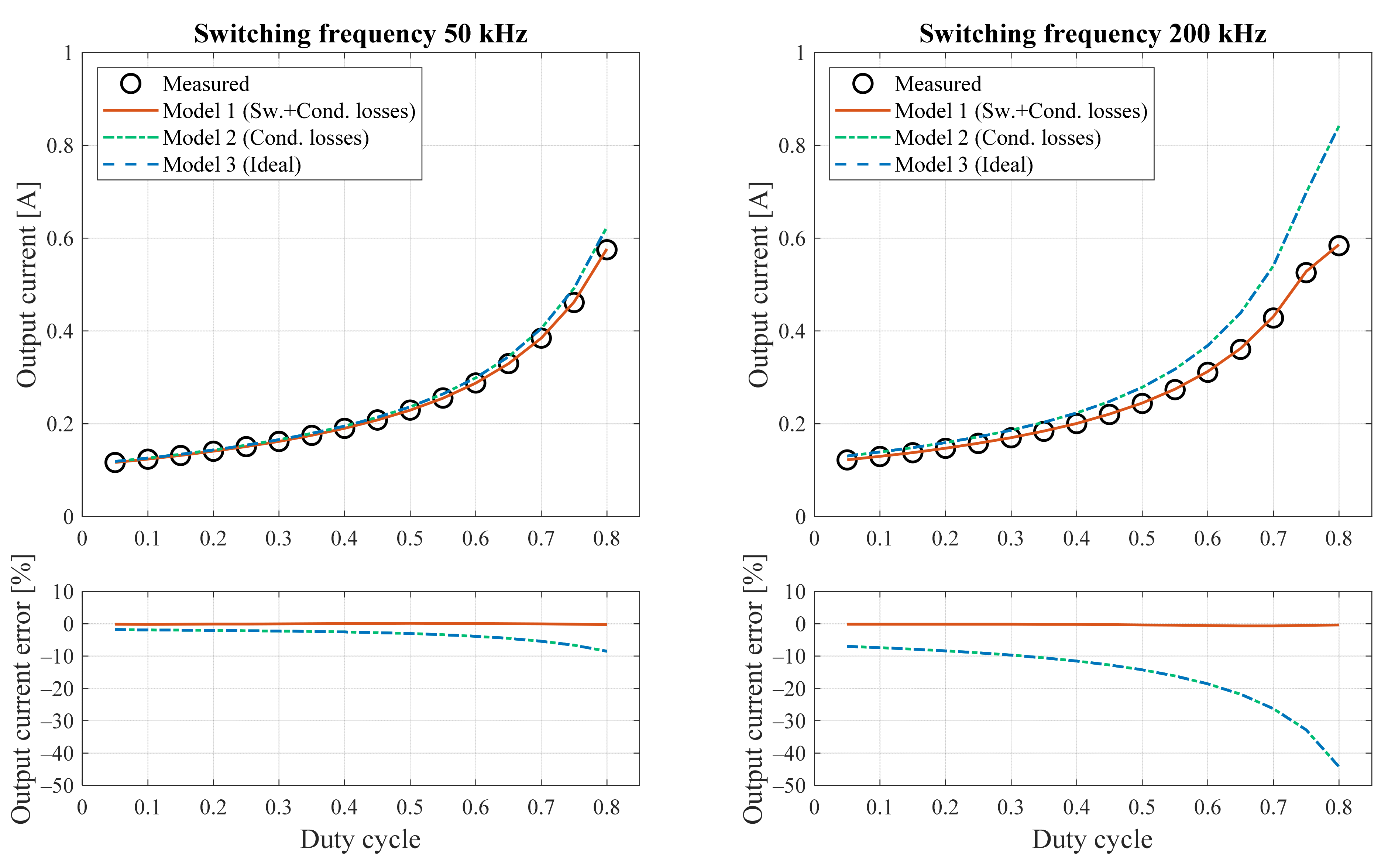
Figure 16 compares the output currents estimated by the models with the measurement results, in addition to the relative errors with a switching frequency of 50 kHz and 200 kHz. The maximum error of the proposed Model 1 is slightly higher than 0.7%, while Model 2 and Model 3 have a maximum error of more than 8% and 44% when the switching frequency is 50 kHz and 200 kHz, respectively.
According to
Section 3, for some applications it is useful to predict the output voltage (or current) from the input quantities and the output current (or voltage). In this case, applying Model 1 results in (12) and (14). As before, the expressions for Model 2 can be obtained from (12) and (14) by assuming
δp = 0, while those for Model 3 can be derived by setting to zero all the parasitic parameters.
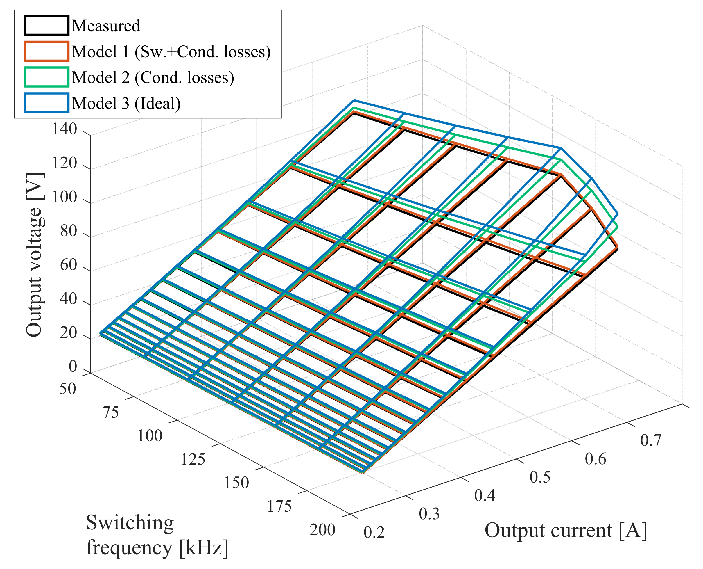
Figure 17 reports the measured and estimated output voltage using Models 1, 2, and 3 as a function of the switching frequency and output current. The output voltage decreases when the switching frequency is equal to 200 kHz because of the power supply current limit. As expected, output current and voltage are proportional, since a resistive load has been connected to the power electronics converter. The voltage predicted by Model 1 is very close to the measured one, while Model 3 shows the higher errors; Model 2 lies somewhere in between. The reason is that both the conduction losses and the finite duration of the switching transients produce a reduction of the output voltage for a given condition.
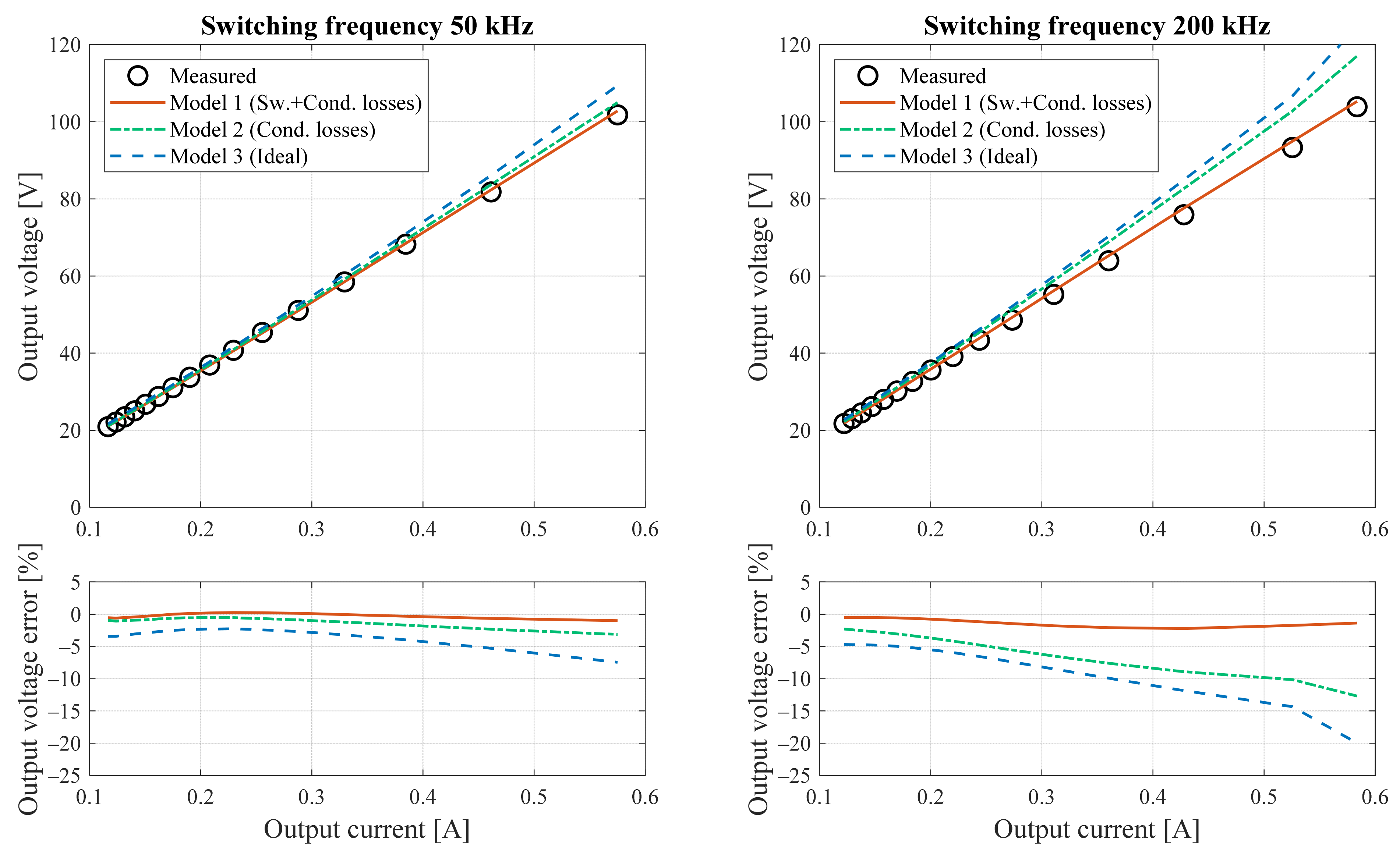
The predicted output voltage and the errors with respect to the measurements at the lowest and highest considered switching frequencies are reported in
Figure 18. Model 1 performs very well in both conditions, since the error remains below 1.1% and 1.6% for 50 kHz and 200 kHz. When
fsw = 50 kHz, the output voltage estimated by using Model 2 is fairly close to the measurements, since the maximum error is slightly above 3%; the voltage error is considerably higher for Model 3, being greater than 7%. At the highest switching frequency, the voltages predicted by both Model 2 and Model 3 are affected by significant errors, because of the increased impact of the switching transients. In particular, the maximum errors are now higher than 15% and 20% for Model 2 and Model 3, respectively.
Similar considerations apply when the three models are employed to predict the output current, starting from the input quantities and the output current. However, for the sake of brevity they are not reported in this paper.
6. Conclusions
The increasing presence of renewable energy sources, energy storages and distributed MPPT algorithms have led to the broad use of boost DC/DC converters. The step-up converter has been well known since the 1970s and, starting from the ideal behavior, different models have been presented in literature to include most of the non-ideal effects such as voltage drops, current leakages, conduction losses and switching losses. Focusing on the switching losses, their effect has been always studied with the target of estimating the global efficiency of the converter. Few studies have been proposed to understand how the switching transients affect the output voltage and current. Among these, no studies have taken into account the possibility that the switching transients affect the output current average value and not only the output voltage. Knowledge of the impact of the switching losses on the input-output voltage and current characteristics could be very important in several applications, in particular to optimize control algorithms for an effective exploitation of renewable energy sources. In this paper, a simple model capable of taking into account the effect of conduction and switching losses on output voltage and current of DC/DC converters has been proposed. In this way, it is possible to represent the effect of all the losses, both due to conduction and switching, on the actual duty cycle of the converter that, because of the losses, may differ from that of the PWM control signal. The accuracy of the proposed model has been evaluated by means of an experimental activity performed on a typical boost converter. In comparison with the traditional models, the voltage and currents predicted by the proposed one are much closer to the measurements, especially when high switching frequencies are adopted (above 100 kHz), thus when switching losses become more relevant. It is worth noting that the approach used to obtain the new model is general and can be applied to any other topology of switch-mode power converter operating under continuous conduction.


