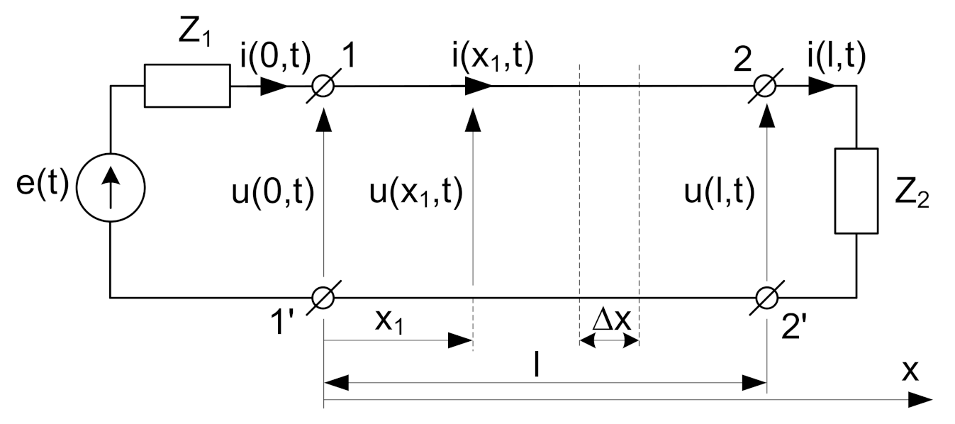
Figure 1.
Model of a two-wire transmission line.
Figure 1.
Model of a two-wire transmission line.
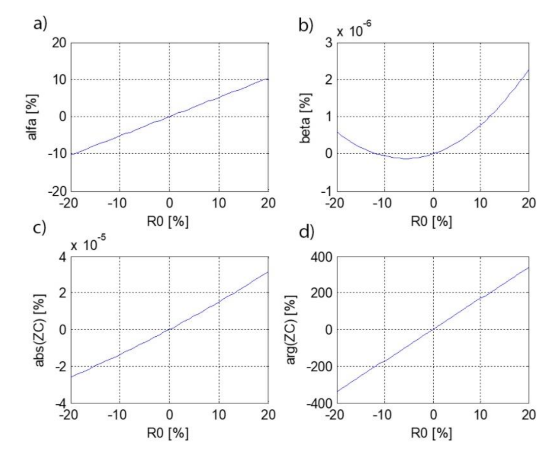
Figure 2.
Changes of wave parameters depending on R0 at f = 100 kHz; (a) damping factor α, (b) phase factor β, (c) wave impedance modulus, and (d) wave impedance argument.
Figure 2.
Changes of wave parameters depending on R0 at f = 100 kHz; (a) damping factor α, (b) phase factor β, (c) wave impedance modulus, and (d) wave impedance argument.
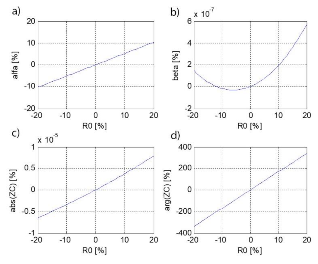
Figure 3.
Changes of wave parameters depending on R0 at f = 500 kHz; (a) damping factor α, (b) phase factor β, (c) wave impedance modulus, and (d) wave impedance argument.
Figure 3.
Changes of wave parameters depending on R0 at f = 500 kHz; (a) damping factor α, (b) phase factor β, (c) wave impedance modulus, and (d) wave impedance argument.
Figure 4.
Changes of wave parameters depending on R0 at f = 1 MHz; (a) damping factor α, (b) phase factor β, (c) wave impedance modulus, and (d) wave impedance argument.
Figure 4.
Changes of wave parameters depending on R0 at f = 1 MHz; (a) damping factor α, (b) phase factor β, (c) wave impedance modulus, and (d) wave impedance argument.
Figure 5.
Changes of wave parameters depending on L0 at f = 100 kHz; (a) damping factor α, (b) phase factor β, (c) wave impedance modulus, and (d) wave impedance argument.
Figure 5.
Changes of wave parameters depending on L0 at f = 100 kHz; (a) damping factor α, (b) phase factor β, (c) wave impedance modulus, and (d) wave impedance argument.
Figure 6.
Changes of wave parameters depending on L0 at f = 500 kHz; (a) damping factor α, (b) phase factor β, (c) wave impedance modulus, and (d) wave impedance argument.
Figure 6.
Changes of wave parameters depending on L0 at f = 500 kHz; (a) damping factor α, (b) phase factor β, (c) wave impedance modulus, and (d) wave impedance argument.
Figure 7.
Changes of wave parameters depending on L0 at f = 1 MHz; (a) damping factor α, (b) phase factor β, (c) wave impedance modulus, and (d) wave impedance argument.
Figure 7.
Changes of wave parameters depending on L0 at f = 1 MHz; (a) damping factor α, (b) phase factor β, (c) wave impedance modulus, and (d) wave impedance argument.
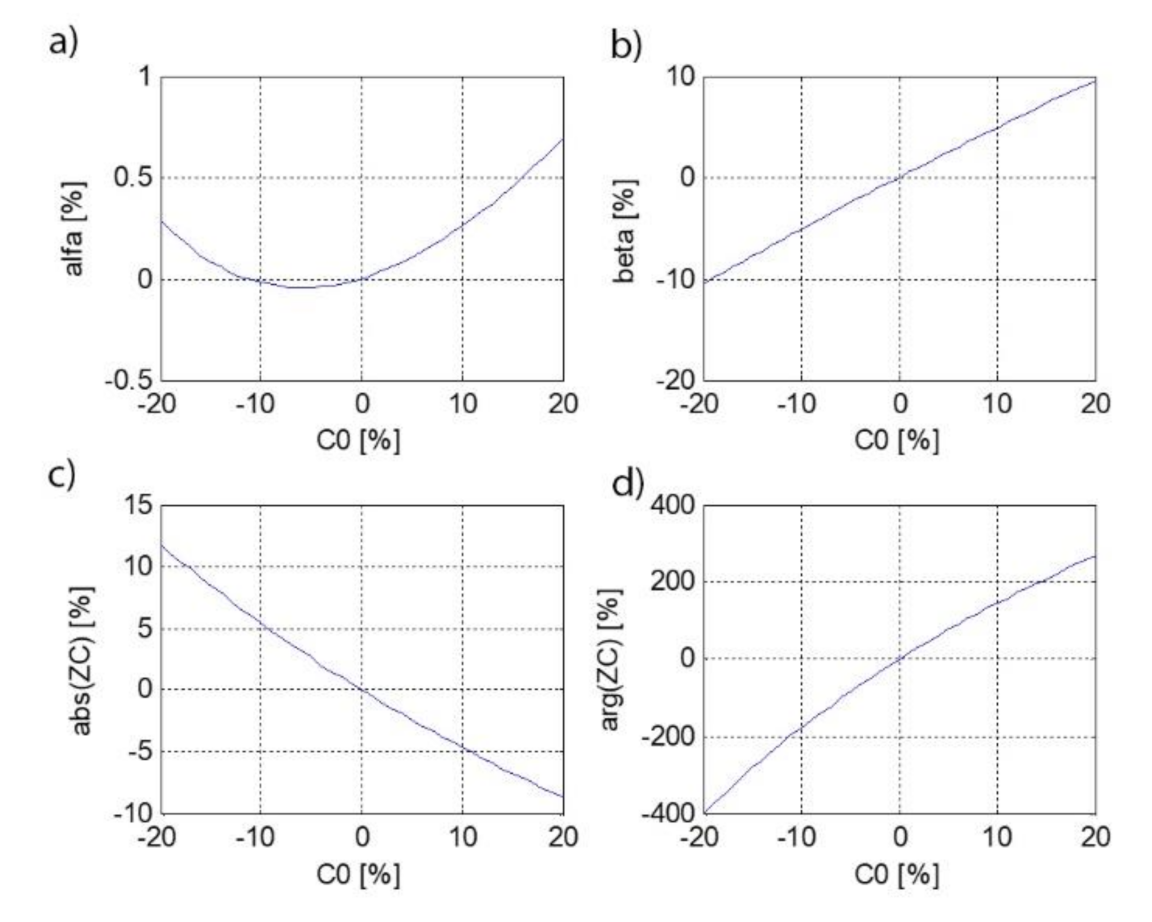
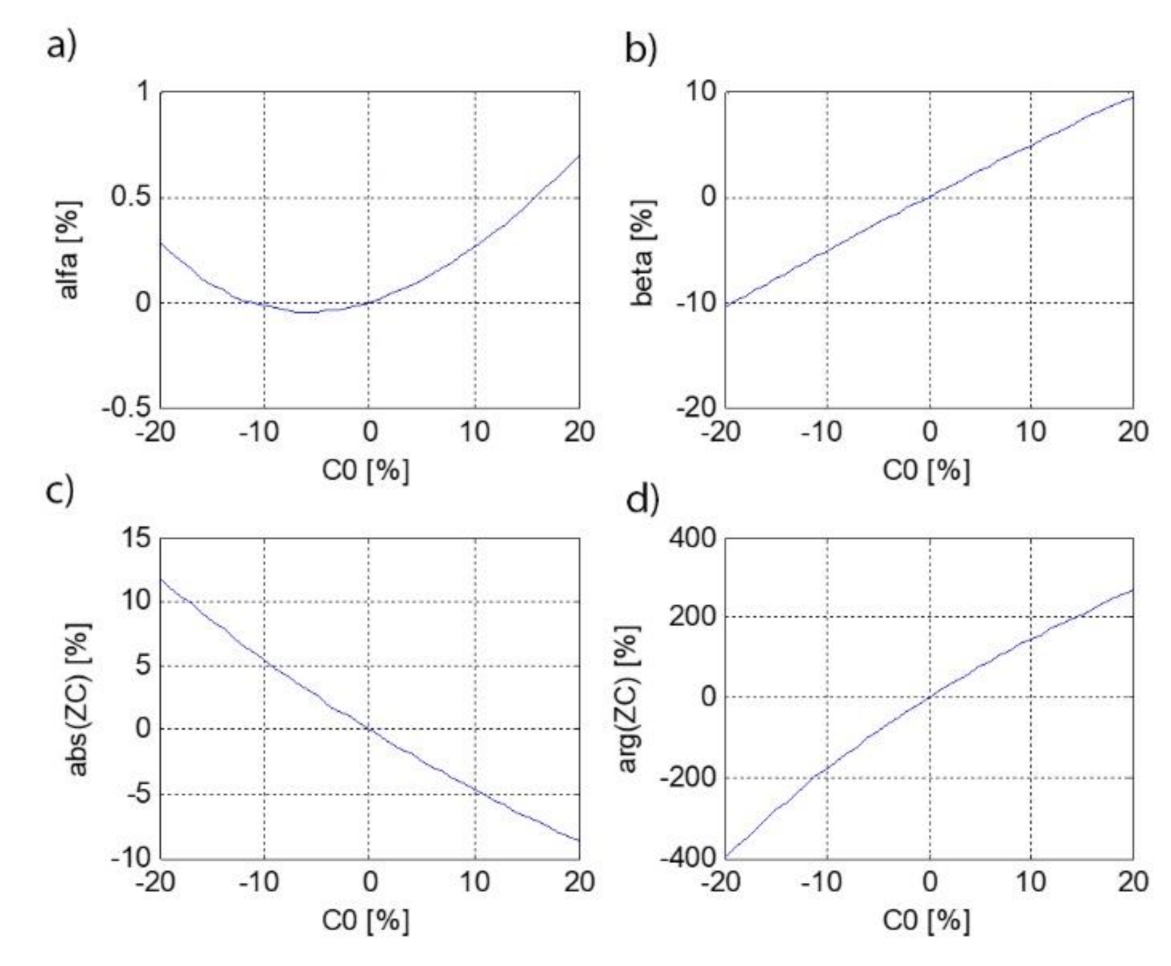
Figure 8.
Changes of wave parameters depending on C0 at f = 100 kHz; (a) damping factor α, (b) phase factor β, (c) wave impedance modulus, and (d) wave impedance argument.
Figure 8.
Changes of wave parameters depending on C0 at f = 100 kHz; (a) damping factor α, (b) phase factor β, (c) wave impedance modulus, and (d) wave impedance argument.
Figure 9.
Changes of wave parameters depending on C0 at f = 500 kHz; (a) damping factor α, (b) phase factor β, (c) wave impedance modulus, and (d) wave impedance argument.
Figure 9.
Changes of wave parameters depending on C0 at f = 500 kHz; (a) damping factor α, (b) phase factor β, (c) wave impedance modulus, and (d) wave impedance argument.
Figure 10.
Changes of wave parameters depending on C0 at f = 1 MHz; (a) damping factor α, (b) phase factor β, (c) wave impedance modulus, and (d) wave impedance argument.
Figure 10.
Changes of wave parameters depending on C0 at f = 1 MHz; (a) damping factor α, (b) phase factor β, (c) wave impedance modulus, and (d) wave impedance argument.
Figure 11.
Changes of wave parameters depending on G0 at f = 100 kHz; (a) damping factor α, (b) phase factor β, (c) wave impedance modulus, and (d) wave impedance argument.
Figure 11.
Changes of wave parameters depending on G0 at f = 100 kHz; (a) damping factor α, (b) phase factor β, (c) wave impedance modulus, and (d) wave impedance argument.
Figure 12.
Changes of wave parameters depending on G0 at f = 500 kHz; (a) damping factor α, (b) phase factor β, (c) wave impedance modulus, and (d) wave impedance argument.
Figure 12.
Changes of wave parameters depending on G0 at f = 500 kHz; (a) damping factor α, (b) phase factor β, (c) wave impedance modulus, and (d) wave impedance argument.
Figure 13.
Changes of wave parameters depending on G0 at f = 1 MHz; (a) damping factor α, (b) phase factor β, (c) wave impedance modulus, and (d) wave impedance argument.
Figure 13.
Changes of wave parameters depending on G0 at f = 1 MHz; (a) damping factor α, (b) phase factor β, (c) wave impedance modulus, and (d) wave impedance argument.
Figure 14.
Changes of wave parameters depending on R0 at f = 100 kHz; (a) U2 voltage modulus, (b) U2 argument, (c) I2 modulus, (d) I2 argument.
Figure 14.
Changes of wave parameters depending on R0 at f = 100 kHz; (a) U2 voltage modulus, (b) U2 argument, (c) I2 modulus, (d) I2 argument.
Figure 15.
Changes of wave parameters depending on R0 at f = 500 kHz; (a) U2 voltage modulus, (b) U2 argument, (c) I2 modulus, (d) I2 argument.
Figure 15.
Changes of wave parameters depending on R0 at f = 500 kHz; (a) U2 voltage modulus, (b) U2 argument, (c) I2 modulus, (d) I2 argument.
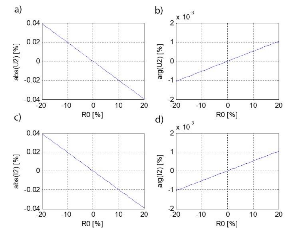
Figure 16.
Changes of wave parameters depending on R0 at f = 1 MHz; (a) U2 voltage modulus, (b) U2 argument, (c) I2 modulus, (d) I2 argument.
Figure 16.
Changes of wave parameters depending on R0 at f = 1 MHz; (a) U2 voltage modulus, (b) U2 argument, (c) I2 modulus, (d) I2 argument.
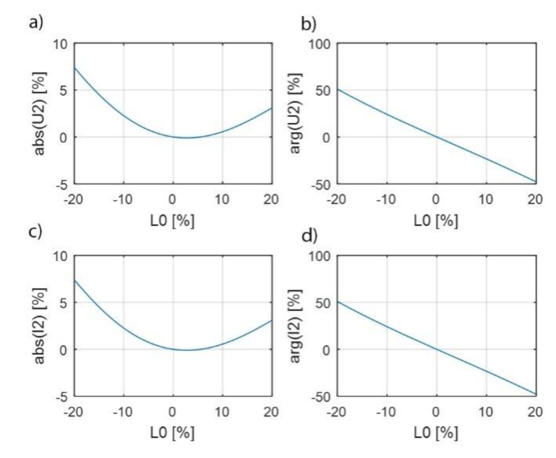
Figure 17.
Changes of wave parameters depending on L0 at f = 100 kHz; (a) U2 voltage modulus, (b) U2 argument, (c) I2 modulus, (d) I2 argument.
Figure 17.
Changes of wave parameters depending on L0 at f = 100 kHz; (a) U2 voltage modulus, (b) U2 argument, (c) I2 modulus, (d) I2 argument.
Figure 18.
Changes of wave parameters depending on L0 at f = 500 kHz; (a) U2 voltage modulus, (b) U2 argument, (c) I2 modulus, (d) I2 argument.
Figure 18.
Changes of wave parameters depending on L0 at f = 500 kHz; (a) U2 voltage modulus, (b) U2 argument, (c) I2 modulus, (d) I2 argument.
Figure 19.
Changes of wave parameters depending on L0 at f = 1 MHz; (a) U2 voltage modulus, (b) U2 argument, (c) I2 modulus, (d) I2 argument.
Figure 19.
Changes of wave parameters depending on L0 at f = 1 MHz; (a) U2 voltage modulus, (b) U2 argument, (c) I2 modulus, (d) I2 argument.
Figure 20.
Changes of wave parameters depending on C0 at f = 100 kHz; (a) U2 voltage modulus, (b) U2 argument, (c) I2 modulus, (d) I2 argument.
Figure 20.
Changes of wave parameters depending on C0 at f = 100 kHz; (a) U2 voltage modulus, (b) U2 argument, (c) I2 modulus, (d) I2 argument.
Figure 21.
Changes of wave parameters depending on L0 at f = 500 kHz; (a) U2 voltage modulus, (b) U2 argument, (c) I2 modulus, (d) I2 argument.
Figure 21.
Changes of wave parameters depending on L0 at f = 500 kHz; (a) U2 voltage modulus, (b) U2 argument, (c) I2 modulus, (d) I2 argument.
Figure 22.
Changes of wave parameters depending on L0 at f = 1 MHz; (a) U2 voltage modulus, (b) U2 argument, (c) I2 modulus, (d) I2 argument.
Figure 22.
Changes of wave parameters depending on L0 at f = 1 MHz; (a) U2 voltage modulus, (b) U2 argument, (c) I2 modulus, (d) I2 argument.
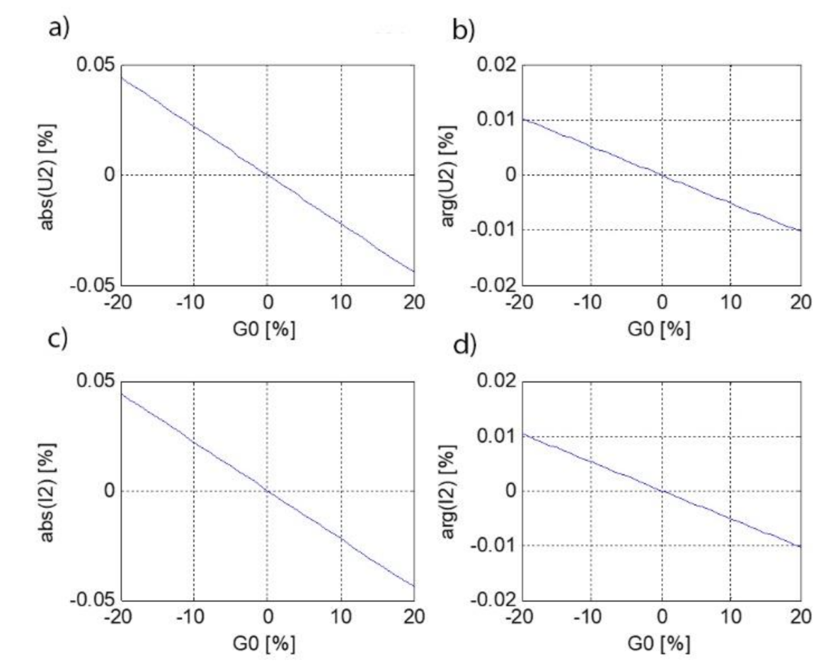
Figure 23.
Changes of wave parameters depending on G0 at f = 500 kHz; (a) U2 voltage modulus, (b) U2 argument, (c) I2 modulus, (d) I2 argument.
Figure 23.
Changes of wave parameters depending on G0 at f = 500 kHz; (a) U2 voltage modulus, (b) U2 argument, (c) I2 modulus, (d) I2 argument.
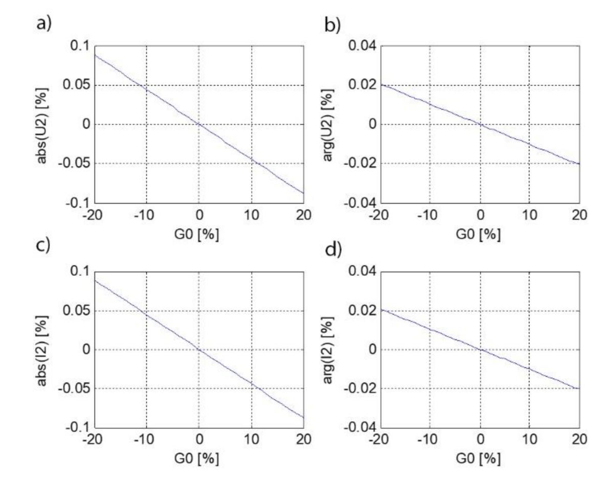
Figure 24.
Changes of wave parameters depending on G0 at f = 1 MHz; (a) U2 voltage modulus, (b) U2 argument, (c) I2 modulus, (d) I2 argument.
Figure 24.
Changes of wave parameters depending on G0 at f = 1 MHz; (a) U2 voltage modulus, (b) U2 argument, (c) I2 modulus, (d) I2 argument.
Table 1.
Changes to the wave impedance modulus.
Table 1.
Changes to the wave impedance modulus.
|
|---|
| | +1% | −1% |
| R0 | 8.980621718802 × 10⁻⁶ | −8.891264700064 × 10⁻⁶ |
| G0 | −7.95516852989 × 10⁻⁶ | 7.876015737812 × 10⁻⁶ |
| L0 | 0.498747363629691 | −0.501247263019991 |
| C0 | −0.496273219279826 | 0.503773449510121 |
Table 2.
Changes to damping constant.
Table 2.
Changes to damping constant.
|
|---|
| | +1% | −1% |
| R0 | 0.515151228520686 | −0.515151275908188 |
| G0 | 0.484848713525002 | −0.484848750704316 |
| L0 | −0.013838466672733 | 0.016490175659639 |
| C0 | 0.016313672812472 | −0.013964997756260 |
Table 3.
Changes to phase constant.
Table 3.
Changes to phase constant.
|
|---|
| | +1% | −1% |
| R0 | 2.85161812570 × 10⁻⁷ | −2.4048216284705 × 10⁻⁷ |
| G0 | −2.27573141879 × 10⁻⁷ | 2.6715112510711 × 10⁻⁷ |
| L0 | 0.49875597170012 | −0.5012560025127765 |
| C0 | 0.49875647683926 | −0.5012565178567181 |
Table 4.
Changes to the real part of the input resistance.
Table 4.
Changes to the real part of the input resistance.
|
|---|
| | +1% | −1% |
| R0 | 0.000384588324788 | −0.0003889650747472 |
| G0 | 0.043391174085347 | −0.0433956466098439 |
| L0 | −5.732231738707145 | 5.9768553112726378 |
| C0 | 3.562167621061453 | −3.2793821336200557 |
Table 5.
Changes to the imaginary part of the input resistance.
Table 5.
Changes to the imaginary part of the input resistance.
|
|---|
| | +1% | −1% |
| R0 | −0.002777179953811 | 0.0027783246452566 |
| G0 | 0.001528422276180 | −0.0015294640405447 |
| L0 | −0.041812016570611 | −0.0221985063733944 |
| C0 | −1.189631026642754 | 1.2554145000339767 |
Table 6.
Changes to the I1 current modulus.
Table 6.
Changes to the I1 current modulus.
|
|---|
| | +1% | −1% |
| R0 | 0.002747571139330 | −0.0027486055903140 |
| G0 | −0.000971236507435 | 0.0009719814772497 |
| L0 | −0.031856013256254 | 0.0939895328519183 |
| C0 | 1.233753020617313 | −1.2645765148497845 |
Table 7.
Changes to the argument of the current I1.
Table 7.
Changes to the argument of the current I1.
|
|---|
| | +1% | −1% |
| R0 | 0.002372834589791 | −0.0023694989848461 |
| G0 | −0.044547012164130 | 0.0445533464751429 |
| L0 | 5.724421549430766 | −5.9109167085244178 |
| C0 | −2.381912054750487 | 1.9818184348223934 |
Table 8.
Changes to the U2 voltage modulus.
Table 8.
Changes to the U2 voltage modulus.
|
|---|
| | +1% | −1% |
| R0 | −0.009870362379686 | 0.0098708010242115 |
| G0 | −0.010998843739695 | 0.0110003885878087 |
| L0 | −0.053850964577535 | 0.0838634668968119 |
| C0 | 0.630798491006207 | −0.6478547211964083 |
Table 9.
Changes to the argument of the voltage U2.
Table 9.
Changes to the argument of the voltage U2.
|
|---|
| | +1% | −1% |
| R0 | 0.000288807602249 | −0.000288916464849 |
| G0 | −0.002528487115057 | 0.002528654755186 |
| L0 | −2.317110575876312 | 2.323205351184315 |
| C0 | −2.751776829843434 | 2.741194932584926 |
Table 10.
Changes to the I2 current modulus.
Table 10.
Changes to the I2 current modulus.
|
|---|
| | +1% | −1% |
| R0 | −0.009870362379715 | 0.0098708010242179 |
| G0 | −0.010998843739739 | 0.0110003885878038 |
| L0 | −0.053850964577548 | 0.0838634668968006 |
| C0 | 0.630798491006164 | −0.6478547211963962 |
Table 11.
Changes to the argument of the current I2.
Table 11.
Changes to the argument of the current I2.
|
|---|
| | +1% | −1% |
| R0 | 0.000288807602261 | −0.0002889164648371 |
| G0 | −0.002528487115069 | 0.0025286547551618 |
| L0 | −2.317110575876356 | 2.3232053511843256 |
| C0 | −2.751776829843455 | 2.7411949325849654 |


 ,
, 


