Article

An Embedded Half-Bridge Γ-Z-Source Inverter with Reduced Voltage Stress on Capacitors

by
Hamed Mashinchi Maheri
1,
Dmitri Vinnikov
1,*,
Mohsen Hasan Babayi Nozadian
2,
Elias Shokati Asl
2,
Ebrahim Babaei
2 and
Andrii Chub
1
1
Power Electronics Research Group, Department of Electrical Power Engineering and Mechatronics, Tallinn University of Technology, 19086 Tallinn, Estonia
2
Faculty of Electrical and Computer Engineering, University of Tabriz, Tabriz 51664, Iran
*
Author to whom correspondence should be addressed.
Energies 2021, 14(19), 6433; https://doi.org/10.3390/en14196433
Submission received: 7 July 2021 / Revised: 20 September 2021 / Accepted: 28 September 2021 / Published: 8 October 2021
(This article belongs to the Special Issue Impedance Source Converters: Topologies, Control, and Applications)

Abstract

:
In this paper, an embedded half-bridge Z-source inverter based on gamma structure is proposed. In contrast with the classical half-bridge inverter, the proposed inverter can generate zero voltage levels in output. High voltage gain and low voltage stress on capacitors are the main advantages of the proposed converter. The value of the boost factor in the proposed structure is increased by changing both the shoot-through (ST) duty cycle and turns ratio of the transformer. The operating principle of the proposed converter in four operating modes is presented. We also calculate the critical inductance and compare the proposed converter with conventional topologies. In addition, power loss and THD analysis are presented. Finally, PSCAD/EMTDC software is used to verify the correct operation of the proposed inverter and the experimental results.

Graphical Abstract

1. Introduction

The Z-source network is one of the important networks in power electronic converters. This network can be used in dc/dc, dc/ac, ac/dc, and ac/ac power conversion. Among the four mentioned types of power conversion, the utilization of the Z-source network in dc/ac power conversion gives significant benefits; hence, the Z-source inverter (ZSI) has been discussed in [1]. The conventional ZSI has an X-shaped impedance network and its Z-source network has two inductors, two capacitors, and one diode. A quasi-Z-source inverter (QZSI) with better features has been presented in [2]. Among these benefits, one can note the reduction in voltage stress and the reduction in input current ripple. In order to decrease the inrush current of the converter in startup, the improved ZSI (IZSI) has been presented in [3]. In [4], the cascaded arrangement of several Z-source networks with low voltage stress on capacitors led to multiple-series Z-source inverters. To increase the boost factor of the presented topology in [4], several networks are required, leading to high volume and high cost.
In some of the articles, Z-source converters have been categorized based on the type of Z-source network of the converter. In general, the impedance networks of the Z-source converters are categorized as conventional Z-source networks and switched Z-source networks [5]. The main difference between these two types of Z-source networks is the existence of a power switch in the switched Z-source converters. To reduce the number of passive elements, a switched boost inverter (SBI) has been presented in [6]. The impedance network of SBI has one inductor, one capacitor, two diodes, and a power switch, and its boost factor is lower than that of ZSI [1]. In order to improve the boost factor of SBI, a current-fed switched inverter (CFSI) has been proposed in [7]. CFSI has the same boost factor as ZSI [1] and a low input current ripple. A high boost factor has been achieved in [8] by using switched-inductor cells. Another topology for a switched Z-source inverter has been presented in [9], which has several passive and semiconductor elements. The reported topology in [9] has two inductors, two capacitors, four diodes, and one power switch in the impedance network. All proposed topologies in [1,2,3,4,5,6,7,8,9] can be used as a full-bridge inverter; however, the extension of the Z-source concept to a half-bridge inverter is possible. The half-bridge Z-source inverters feature the same operation as full-bridge inverters but with a two-times lower number of power switches than the full-bridge topology. In [10], a Z-source half-bridge converter with the aim of application in the electrochemical industry has been presented. In [11], a half-bridge Z-source inverter with two Z-source networks has been presented. This topology does not have a high boost factor in comparison with a conventional Z-source inverter but it features low voltage stress of the components. In [12], another topology for a half-bridge Z-source inverter has been presented, but it needs more Z-networks to achieve a high boost factor. The half-bridge switched boost inverter (HF-SBI) has been proposed in [13]. Steady-state analysis and small signal analysis of HF-SBI has been presented in [13]. With the same value of the input voltage and duty cycle, the boost factor of HF-SBI is higher than that of SBI [6] but the input current ripple of HF-SBI is still high. Two different switched half-bridge Z-source inverters have been presented in [14,15]. These topologies have a high boost factor in comparison with conventional topologies, but the use of power switches can lead to complexity in switching and modulation techniques.
Extension of half-bridge Z-source and switched Z-source inverters to a half-bridge transformer-based Z-source inverter is possible [16]. The transformer-based Z-source inverters can control the boost factor of the converter by two parameters, the shoot-through duty cycle and the turns ratio of the transformer [17,18]. A trans-Z-source neutral point clamped inverter has been presented in [19], which is composed of two impedance networks. A transformer based on the presented structures in [7,8] has been introduced in [20,21]. In [20], two types of trans-switched boost inverters have been presented with the same value of the boost factor. A variation of the presented structures in [20] has been proposed in [21]. The number of the elements in [20,21] is the same; however, in the presented structure in [21], a lower turns ratio is needed for increasing the voltage. Furthermore, the cascaded topologies for Z-source inverters based on the transformer and tapped inductors have been presented [22]. A half-bridge trans-Z-source inverter has been reported in [23]. The proposed concept features a continuous input current with a high voltage boost factor. However, comparing the counterparts, the number of components is greater and the converter features high voltage stress of the capacitors.
In this paper, a new embedded topology for the half-bridge Γ-Z-source inverter is proposed. Compared with the conventional Γ-Z-source full-bridge inverter, the input power source is connected in series with power switches instead of a series connection with diodes. The proposed concept features a high boost factor compared to the conventional Z-source inverters. Further, low capacitor voltage stresses and low switching voltage spikes are achieved with the proposed configuration. The paper is organized as follows.
In Section 2, the topology and operating principle of the proposed converter are presented. The design considerations of the magnetic components and capacitors are given in Section 3. In addition, the calculation of power losses and total harmonic distortion is provided in Section 4. A detailed comparison with the other related topologies is presented in Section 5. The power losses and efficiency are evaluated in Section 6. Section 7 validates the effectiveness of the proposed concept using simulation. The control scheme and dynamic of the proposed converter are studied in Section 8. Finally, experimental results are used to verify the correctness of the theoretical analysis in different operating modes.

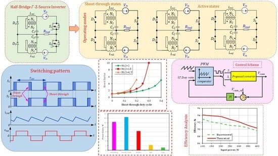
2. Proposed Topology

The power circuit of the proposed topology is shown in Figure 1. The proposed topology has two transformers with a turns ratio of N12 = N1/N2, diodes D1 and D2, and capacitors C1 and C2. Similar to the classic half-bridge inverter, the proposed half-bridge inverter has two voltage sources and two switches. In the proposed topology, the magnetizing inductances of the transformers are equal (Lm1 = Lm2 = Lm) and C1 = C2 = C. The values of voltage across primary windings in the upper and lower networks (vp1 = vp2 = vp) are equal. Hence, the following summarization can be considered:
v p 1 = v n 1 = v 1
v p 2 = v n 2 = v 2
V C 1 = V C 2 = V C
v D 1 = v D 2 = v D

2.1. Operating Principle

The operating modes of the proposed inverter are specified by turning on and turning off the diodes and power switches. The number of operating modes in the proposed inverter is four. Figure 2 shows the equivalent circuit of the proposed converter in operation modes. In the first operating mode, both switches S1 and S2 are on; so, the proposed inverter is in shoot-through (ST) state. In the second operating mode, switch S1 is on and switch S2 is off; hence, the proposed inverter is in non-shoot-through state. In the third operating mode, similar to the first operating mode, both switches S1 and S2 are on; so, the proposed inverter is in ST state. In the fourth operating mode, switch S1 is off and switch S2 is on. It is important to note that, in the theoretical analysis, all of the elements are assumed to be ideal. More precisely, the following items are considered in the theoretical calculations:
  • The series resistance and the voltage drop of the switches and the diodes are ignored;
  • The series resistance and the capacitors and the inductors are ignored;
  • The internal resistance of the input voltage is ignored;
  • The switching method and the turning on and off of semiconductor elements are assumed to be ideal;
  • The load of the proposed converter is pure ohmic with resistance R.
In the following, the operating principle and detailed analyses are given.

2.1.1. First Operating Mode

The ST state occurs in the first operating mode and both switches are on but both diodes are off. By applying Kirchhoff’s voltage law (KVL) in both the upper and lower networks, the following equations are obtained:
V C + v 2 v 1 + V i v o
V C + v o + V i v 1 + v 2 = 0
By using Equations (5) and (6), the average voltage across the capacitors and the output voltage are obtained as follows:
V C = v 1 v 2 V i = ( 1 N 2 N 1 ) v 1 V i
v o = 0
In this operating mode, due to the positive value of the voltage across the magnetizing inductor L m , the magnetizing current linearly increases from its minimum value (IL,min) to its maximum value (IL,max). By considering Equation (7), the magnetizing current is obtained as follows:
i L m = v 1 L m t + I L , min = N 1 ( V C + V i ) ( N 1 N 2 ) L m t + I L , min
By considering i p 1 = i n 1 = i 1 , i p 2 = i n 2 = i 2 and Kirchhoff’s current law (KCL), the following equation can be written:
i 2 = i 1 + i L m
Since i2 = (N1/N2)i1, the current through the capacitor C1 is calculated as follows:
i C 1 = i 2 = N 1 N 1 N 2 i L m

2.1.2. Second Operating Mode

In the second operating mode, switch S1 is on, and switch S2 is off. The diodes are on. By using KVL, the obtained equations are as follows:
V C = v 2 = N 2 N 1 v 1
v o = v o , max = V i v 1 = V i N 1 N 2 v 2
In this operating mode, due to the negative value of the voltage across the magnetizing inductor, the magnetizing current linearly decreases from its maximum value (IL,max) to its minimum value (IL,min). By using Equation (12), the magnetizing current is obtained as:
i L m = v 1 L m t + I L , max = N 1 V C N 2 L m t + I L , max
By using KCL, the following equation is obtained as follows:
i p 1 + i L m = v o , max R
where R is the load resistance.
The current of capacitor C1 is obtained by Equation (16):
i C 1 = N 1 N 2 ( i L m v o , max R )

2.1.3. Third Operating Mode

In the third operating mode, both diodes are off, but both switches are on. Due to the similarity of the analysis in this operating mode to the first operating mode and to avoid prolongation, detailed analysis is omitted.

2.1.4. Fourth Operating Mode

In the fourth operating mode, switch S1 is off, and switch S2 is on. Both of the diodes are on. By using KVL, the following equation is obtained by Equation (17):
v o = v o , min = v o , max = v 1 V i
The current through the capacitor C1 is calculated as follows:
i C 1 = i p 2 = N 1 N 2 i p 1 = N 1 N 2 i L m
Figure 3a shows a logical diagram and waveforms of the switching pattern. Figure 3b shows waveforms of the current and voltage in the proposed inverter.

2.2. Boost Factor

The average voltage across the magnetizing inductor in steady state is zero; hence, the following equation can be written:
0 T s v 1 d t = 0
By using Equations (7), (12), and (19), the following equation is derived:
N 1 ( V C + V i ) N 1 N 2 D S T T s N 1 V C N 2 ( 1 D S T ) T s = 0
where DST and TS are the ST duty cycle and switching period, respectively.
From Equation (20), the average voltage across the capacitors is calculated as follows:
V C = D S T N 12 ( 1 D S T ) 1 V i
where N12 is equal to the ratio of N1/N2 and the range of the ST duty cycle is 0 ≤ DST < 1 − (1/N12).
By using Equations (12), (13), and (21), the maximum output voltage is calculated as follows:
v o , max = N 12 1 N 12 ( 1 D S T ) 1 V i
Due to the definition of the boost factor for the proposed inverter as B = (vo,max/Vi), the following equation for the boost factor is derived:
B = N 12 1 N 12 ( 1 D S T ) 1

3. Design Considerations

In steady state, the average value of the capacitor’s current is zero; hence, the following equation can be written:
0 T s i C d t = 0
From Equations (11), (16), and (24), the following equation can be written:
N 1 N 1 N 2 I L m D S T + N 1 ( 1 D S T ) 2 N 2 ( 2 I L m v o , max R ) = 0
By solving Equation (25), the average current through the magnetizing inductors is obtained as follows:
I L m = ( 1 D S T ) ( N 1 N 2 ) 2 R ( N 1 N 2 N 1 D S T ) v o , max
By using Equations (22) and (26), ILm is calculated as follows:
I L m = ( 1 D S T ) ( N 12 1 ) 2 2 R [ N 12 ( 1 D S T ) 1 ] 2 V i
For a proper design, the ripple of magnetizing current should be calculated. By using of Equation (7), the following equation is written:
L m Δ i L m 0.5 D S T T s = N 1 N 1 N 2 ( V i + V C )
where ∆iLm is the ripple of the magnetizing current.
By using Equations (21) and (28), ∆iLm is obtained as follows:
Δ i L m = N 12 D S T ( 1 D S T ) 2 L m f s [ N 12 ( 1 D S T ) 1 ] V i
To calculate the voltage ripple across capacitors, ∆vC, we use:
Δ v C = N 1 N 2 C 0 0.5 ( 1 D S T ) T s ( v 1 L m t + I L , max ) d t
By solving Equation (30), ∆vC can be written as follows:
Δ v C = N 12 ( N 12 1 ) 2 ( 1 D S T ) 2 4 R C f s [ N 12 ( 1 D S T ) 1 ] 2 V i
By defining the percentage of permissible current ripple of the magnetizing inductance (xLm%) and the percentage of permissible voltage ripple for capacitors (xC%), we have:
x L m % = Δ i L m I L m × 100
x C % = Δ v C V C × 100
By using Equations (27), (29), and (32), xLm% is derived as follows:
x L m % = N 12 D S T R [ N 12 ( 1 D S T ) 1 ] L m f s ( N 12 1 ) 2 × 100
By using Equation (34), the value of the magnetizing inductors is obtained as follows:
L m = N 12 D S T R [ N 12 ( 1 D S T ) 1 ] x L m % f s ( N 12 1 ) 2 × 100
By considering Equations (21), (31), and (33), xC% is derived as follows:
x C % = N 12 ( N 12 1 ) 2 ( 1 D S T ) 2 4 R C f s D S T [ N 12 ( 1 D S T ) 1 ] × 100
Hence, the value of the capacitors can be written as follows:
C = N 12 ( N 12 1 ) 2 ( 1 D S T ) 2 4 R f s x C % D S T [ N 12 ( 1 D S T ) 1 ] × 100
It is noticeable that the calculated inductance from Equation (35) should not lead to improper operating states. It should be mentioned that two operating states can occur in the proposed inverter. In the first operating state, the synchronous operation of diodes (SOD) leads to four operating modes, and D1 and D2 turn on and off simultaneously. Detailed analyses of these operating modes have been described in the previous sections. By selecting a small magnetizing inductance, SOD is disrupted. Asynchronous operation of diodes (AOD) in the second operating state leads to ann asymmetrical output voltage with more than four operating modes. To avoid AOD, the critical inductance (Lm,crit) should be lower than the magnetizing inductance. In the boundary condition between SOD and AOD, the current through diode D1 at the second operating mode reaches zero. Hence, by using Equation (16), the following equation is derived:
i D 1 = i C 1 + i o = N 1 N 2 i L m N 1 v o , max N 2 R + v o , max R = 0
From Equations (14) and (38), the following equation for Lm,crit is calculated:
L m , c r i t = R N 12 2 [ N 12 ( 1 D S T ) 1 ] D S T ( 1 D S T ) 2 f s [ 2 ( N 12 1 ) 2 N 12 ( N 12 1 ) 2 ( 1 D S T ) ]

4. Power Loss and THD Calculation

4.1. Power Loss Calculation

In order to calculate the power loss of the proposed converter, the method that has been presented in [9,24] is used. At first, the power loss of the each element is calculated and then the total power loss is obtained from the sum of them.
The power losses in semiconductor elements are divided into conduction power loss and switching power loss. The voltage and current of the switch (S1) for a period are obtained as follows:
v S 1 = { 0 0 t 0.5 D S T T s ( 1 s t   m o d e ) 0 0 t 0.5 ( 1 D S T T s ) ( 2 n d   m o d e ) 0 0 t 0.5 D S T T s ( 3 r d   m o d e ) 2 | v o , min | 0 t 0.5 ( 1 D S T T s ) ( 4 t h   m o d e )
i S 1 = { N 1 N 1 N 2 I L m 0 t 0.5 D S T T s ( 1 s t   m o d e ) N 1 N 2 ( v o , max R I L m ) 0 t 0.5 ( 1 D S T T s ) ( 2 n d   m o d e ) N 1 N 1 N 2 I L m 0 t 0.5 D S T T s ( 3 r d   m o d e ) 0 0 t 0.5 ( 1 D S T T s ) ( 4 t h   m o d e )
According to Equation (41), the conduction power loss of the switch S1 is calculated as follows:
P C o n d , S 1 = D S T N 1 N 1 N 2 I L m ( V F , S + N 1 N 1 N 2 r S I L m ) + 0.5 ( 1 D S T ) N 1 N 2 ( v o , max R I L m ) [ V F , S + r s 0.5 N 1 N 2 ( v o , max R I L m ) ]
where rS and VF,S are the series resistance and the voltage drop of the switch in conduction mode, respectively.
By considering Equations (40) and (41), the switching power loss of S1 in ton,S and toff,S (turn-on and turn-off time) is calculated as follows:
P S w o n , o f f = N 1 3 ( N 1 N 2 ) f s B I L m V i ( t o n , S + t o f f , S )
In order to calculate the power loss of the diodes, the voltage and current of the diode D1 should be calculated for a period as follows:
v D 1 = { N 12 V C + V i 1 N 12 0 t 0.5 D S T T s ( 1 s t   m o d e ) 0 0 t 0.5 ( 1 D S T T s ) ( 2 n d   m o d e ) N 12 V C + V i 1 N 12 0 t 0.5 D S T T s ( 3 r d   m o d e ) 0 0 t 0.5 ( 1 D S T T s ) ( 4 t h   m o d e )
i D 1 = { 0 0 t 0.5 D S T T s   ( 1 s t   m o d e ) N 1 N 2 ( I L m v o , max R ) + v o , max R 0 t 0.5 ( 1 D S T T s )   ( 2 n d   m o d e ) 0 0 t 0.5 D S T T s   ( 3 r d   m o d e ) N 1 N 2 I L m 0 t 0.5 ( 1 D S T T s )   ( 4 t h   m o d e )
The conduction and switching loss of the diode D1 are calculated from the below equations.
P C o n d , D 1 = 0.5 ( 1 D S T ) [ N 1 N 2 ( I L m v o , max R ) + v o , max R ] { V F , D + r D [ N 1 N 2 ( I L m v o , max R ) + v o , max R ] } + 0.5 ( 1 D S T ) ( N 1 N 2 I L m ) ( V F , D + r D N 1 N 2 I L m )
P S w , D 1 o f f = N 12 V C + V i 6 ( 1 N 12 ) f s [ 2 N 12 I L m + v o , max R ( 1 N 12 ) ] t o f f , D
where rD and VF,D are the series resistance and the voltage drop of the diodes in conduction mode, respectively.
According to the symmetrical operation of the proposed converter, the power loss of the switch S2 and the diode D2 are the same as the power loss of S1 and D1, respectively.
The power loss of the capacitors is obtained as:
P r C = 1 T s 0 T s r C i C 2 d t
where rC is the internal series resistance capacitors.
By considering the value of i C 1 Equations (11), (16), and (18), the power loss of the capacitors is obtained as follows:
P C 1 = P C 2 = r C 1 [ ( N 1 N 1 N 2 I L m ) 2 D S T + ( 0.5 ( 1 D S T ) N 1 N 2 I L m ) 2 ] + 0.5 r C 1 ( 1 D S T ) ( N 1 N 2 ( I L m v o , max R ) + v o , max R ) 2
The power loss of inductors is expressed by the core loss and conduction power loss. The core power loss is calculated as follows:
P C L = 0.33 B 1.98 f 1.64 V e f f
where B is the flux density, f is the frequency in kHz, and Veff is the effective core volume.
The conduction power loss of inductors is expressed by the values of resistance of inductors (rL) and the RMS current of them as follows:
P r L 1 = P r L 2 = r L I L m 2

4.2. THD Calculation
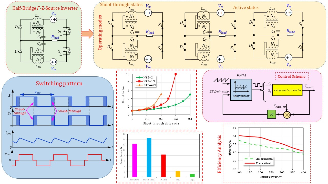
In order to obtain the relation of the total harmonic distortion (THD) for the proposed converter, the Fourier series of the output voltage should be considered as follows:
v o = m = 1 , 3 , 5 , X m sin ( m ω t )
The value of Xm in Equation (52) is calculated from the below equation. It should be noted that because vo is an odd function, the an Fourier coefficient is equal to zero.
X m = 2 T s 0 T s v o s i n ( m ω t ) d ω t = 2 B V i m π [ c o s ( m ω t ) | π 0.5 π D S T 0.5 π D S T ]
By simplifying the above equation, the following equation is obtained:
X m = 4 B V i m π c o s ( 0.5 m π D S T )
The RMS value of the output voltage is calculated from the following equation:
V o , r m s = 1 D S T B V i
Considering Equations (54) and (55), the value of THD is calculated as follows:
T H D = V o , r m s 2 X 1 , r m s 2 X 1 , r m s = 2 V o , r m s 2 X 1 2 X 1
By simplifying the above equation, the value of THD is as follows:
T H D = 2 π 2 ( 1 D S T ) [ 4 c o s ( 0.5 π D S T ) ] 2 4 c o s ( 0.5 π D S T )

5. Comparison

In this section, the proposed converter is compared with the literature regarding the different parameters, such as the boost factor and voltage stress on capacitors. Table 1 shows the relation among the boost factor and the maximum voltage stress across the capacitors in the proposed and the conventional structures.

5.1. Comparison of Boost Factor

The boost factor of the proposed converter depends on two factors. The first factor is the value of the ST duty cycle, and the second factor is the turns ratio of the used transformer. Figure 4a shows the boost factor of the proposed converter for different values of N12. As can be appreciated from Figure 4a, the boost factor increases by increasing the turns ratio of the transformers. In Figure 4b, the boost factor of the proposed converter with N12 = 5/4 is compared with [4,7]. Figure 4c,d show the variation in the boost factor for N12 = 4/3 and N12 = 3/2 with the presented topologies in [1,2,3,5,6,8,9,10,11,12,13,14]. As can be appreciated from Figure 4c, the proposed converter features a high boost factor. For the proposed converter, a boost factor of 10 could be achieved for an ST duty cycle around 0.2, but for the proposed converter in [13,14], it is achievable at an ST duty cycle around 0.3. It is worth mentioning that, for the same condition, the boost factor of the proposed converter could be increased by increasing the turn ratio of the transformers.

5.2. Comparison of Voltage Stress on Capacitors

The voltage stress of the capacitors is one of the parameters that could be considered for the benchmarking of the converters. This value for the proposed converter is lower than some conventional inverters for low values of the ST duty cycle. According to Equation (21), the voltage stress in DST = 0 is close to zero, which results in soft-start capability [25]. Figure 5a shows the normalized value of the voltage stress of the capacitors for different values of N12. The voltage stress of the capacitors for the proposed and conventional inverters is compared in Figure 5b. As can be seen for the turns ratio of N12 = 2, the voltage stress of the capacitors is the lowest for the proposed converter. For the turns ratio of 3/2, it is the lowest for ST duty cycles lower than 0.25, and it increases by increasing the DST.

5.3. Comparison of the Number of Used Elements

Comparison of the number of used elements is one of the most important tasks when comparing topologies. In Table 2, the number of elements in the proposed and conventional inverters is shown. According to Table 2, the proposed topology, similar to conventional Z-source inverters [1,2,3], has two capacitors in the power circuit, but the number of used transformers is double in comparison with Trans ZSI [17]. Of course, the proposed inverter has fewer switches due to the half-bridge structure of the output stage.

5.4. THD Comparison

The THD factor is one of the most important parameters for the evaluation of impedance source inverters. For the proposed converter, THD could be defined by Equation (57). Table 3 compares the estimated THD for the proposed converter and two other structures for different values of the ST duty cycle. The switching control method is the same for all of the structures. For all the converters, THD is the maximum for DST = 0 as the converters do not have zero values at the output. By increasing the ST duty cycle, the THD is decreased as the zero state is produced for the output voltage. The trend demonstrates that by increasing the ST duty cycle from 0 to 0.2 for all the converters, THD is decreased. The THD is improved by around 47% by increasing the ST duty cycle from 0 to 0.2. Comparing the THD for the proposed converter and reported converters in [13,15], it is the lowest for the proposed converter and the highest for the converter presented in [13]. According to this table, it can be seen that changing the value of the turns ratio of the transformer does not have a significant effect on the value of THD.

6. Power Losses and Efficiency Evaluation

Based on the given methodology in Section 4, the power losses of the proposed converter are analyzed. Figure 6 shows the power loss distribution of the proposed converter. The estimation was carried out at the input power of 400 W for the given values in Table 4. As can be appreciated from Figure 6, the power losses of the semiconductors dominate over the power losses of the inductors and capacitors. Around 32% of the power losses are switching losses, and 37% of the dissipated power is for conduction losses in the switches. As can be seen, the switching losses are lower than the conduction losses of the switches. As the proposed converter operates at a low switching frequency, the switching losses are low compared with the conduction losses. The diodes feature a power loss that is lower than the total power losses of the switches. Most of the power losses for diodes are conduction losses, as the used diodes are Schottky barrier diodes; the conduction losses dominate over the turn-off losses of the diodes. Based on the estimated power losses, the efficiency of the proposed converter is 90.35%.
Figure 7 shows the comparison of the estimated efficiency for the proposed converter and the reported converters in [11,16,26]. As can be appreciated from Figure 7, the proposed converter features the highest efficiency. The number of components is same for the proposed converter and [16]. However, the proposed configuration features a low voltage stress in the capacitors and switches that results in high efficiency. The proposed converters in [11,26] feature a higher number of components than the proposed converter and [16]; due to this and the high RMS current of the switches, the efficiency is low for [11,26], with a difference of around 2.5% at the full-load condition. The difference for the part- and full-load conditions is higher than that for the light-load condition, as, for the full-load condition, the conduction losses dominate the switching losses. The efficiency for the proposed converter in [26] is the lowest as the number of components, especially semiconductors, is the highest.

7. Simulation Results

In this section, the given theoretical analysis and operation of the proposed converter are verified using PSCAD/EMTDC software. Selected values of parameters are reported in Table 4. It is noticeable that the selected value for magnetizing inductance is higher than the critical inductance, with a value of 914 µH, which is calculated from equation (39). On the other hand, xLm% and xC% are lower than 70% and 2%, respectively.
Figure 8a shows waveforms of the current through diodes D1 and D2. According to this figure, the current through diodes in the ST state is zero, which is in line with Figure 3b. Figure 8b shows the primary side current, which verifies theoretical concepts. Figure 8c shows the voltage and current of the primary magnetizing inductor. As can be observed from Figure 8c, the voltages in ST and non-ST states are 762.01 V and −190.98 V, which are close to values of 768 V and −192 V calculated from (12) and (17), respectively. The simulated average value and ripple of the magnetizing current are 4.76 A and 3.18 A, which differ slightly from the values of 4.80 A and 3.07 A calculated from (27) and (29). Figure 8d shows the waveform of the capacitors’ current. These waveforms have a 180° phase degree with each other, which is in agreement with theory. Figure 9 shows the voltage across capacitors and the output voltage. According to Figure 9a, voltage ripple and average voltage values across capacitors are 2.57 V and 142.12 V, respectively. The estimated value from Equations (31) and (21) equals 2.56 V and 144 V, indicating minor differences between simulated and estimated values. According to Figure 9b, the output voltage has negative, positive, and zero levels. The maximum value of the output voltage is 237.82 V, which is in line with the value of 240 V calculated from (22). In general, the simulation results are in good agreement with the theoretical results.
Figure 10 shows the simulation results of the proposed converter during the transient state. Figure 9a shows the voltage across capacitor C1. As can be seen, the voltage across the capacitor reaches a steady state after 0.04 s. Figure 9b shows the output voltage waveform at the startup moment. According to this figure, the proposed inverter has stable operation, and the dynamic response is appropriate.

8. Control Scheme and Dynamic Performance

Figure 10 shows the schematic of the control strategy for the proposed converter. The Pulse Width Modulation (PWM) method is used to control the switches. In order to control the maximum value of the output voltage, a PI controller is used. The maximum value of the output voltage of the proposed converter is compared with the desired value of the output voltage (Vo,max_ref), and if there is a difference, it is applied to the controller to produce a desirable duty ratio. The desirable duty ratio is compared with a carrier wave, and then suitable interpolated pulses are produced to the switches. The PI controller has a gain and time constant this parameters are defined by a trade-off. In order to show the stable performance of the proposed converter, the simulated dynamic response of the output voltage for a step change in the input voltage is shown in Figure 11. As can be appreciated from Figure 11, by applying a step change in the input voltage, the converter shows stable performance. By increasing the input voltage when the converter operates in steady state, the feedback control system changes the ST duty cycle to fix the operating point at the constant output voltage, with a maximum value of 240 V when the ST duty cycle is decreased. After a short operation at an input voltage of 58 V, the voltage is step changed to 48 V and the closed-loop control system operates as the maximum value of the output voltage is fixed at 240 V by increasing the duty cycle. The stable operation of the proposed converter could be confirmed by carrying out the step change process.

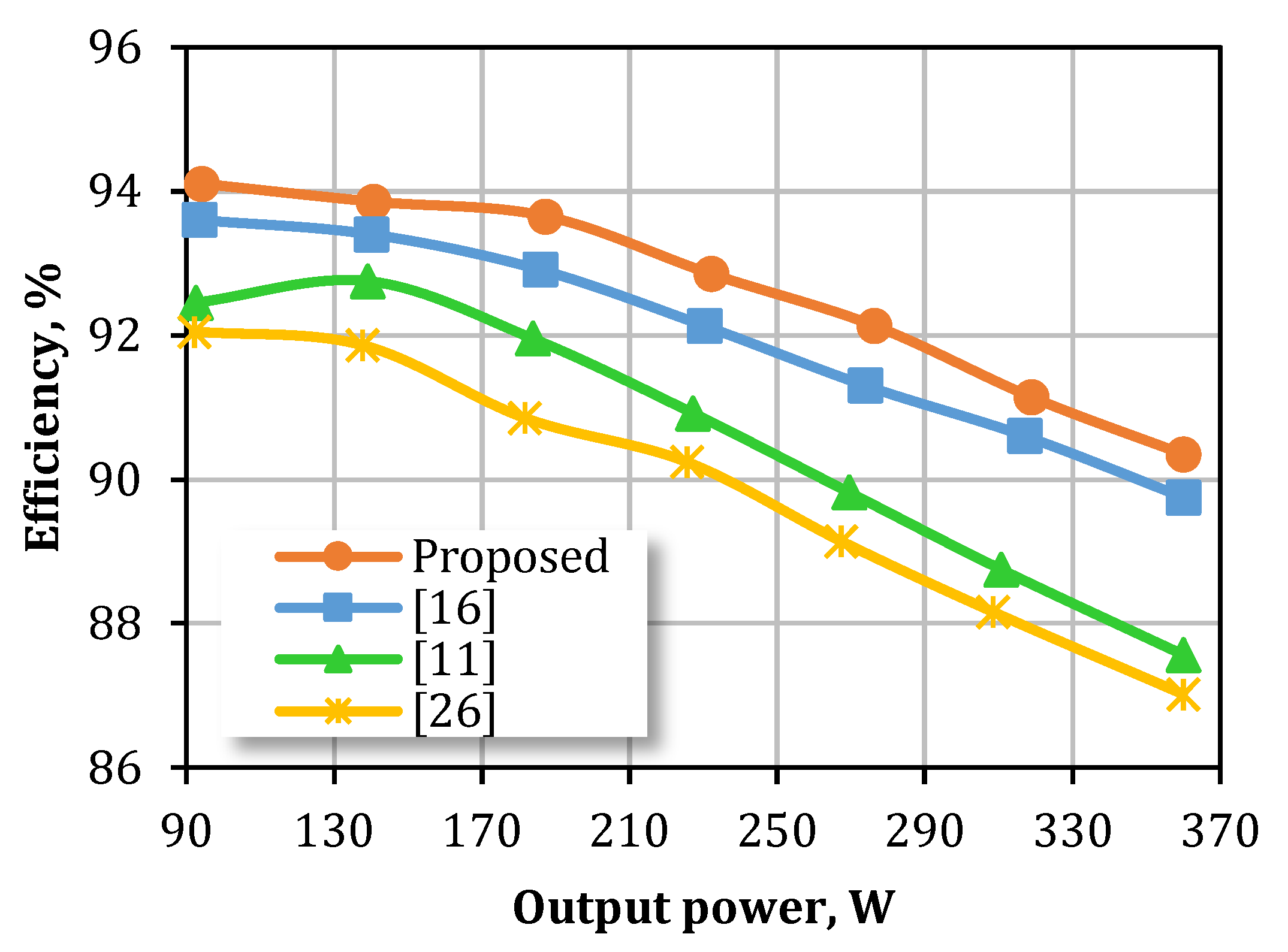
9. Experimental Verification

In this section, experimental results are provided to verify the validity of the theoretical analysis and simulation results. A 400 W prototype (Figure 12) was assembled based on the main schematics of the proposed converter shown in Figure 1. The main specifications and types of semiconductor components used in the prototype are listed in Table 4. The converter was tested at the input voltage of 48 V, which was provided by the power supply EA PSI9080-60. The maximum value of output voltage was regulated to 240 V. The converter was controlled by the microcontroller STM32F334R8T6, utilizing a Cortex-M4 core. The driver circuit consisted of an ACPL-K342 BROADCOM optocoupler and dc-dc converter PEM1-S12-D15-S. The power conversion efficiency was measured with the help of a precision power analyzer, Yokogawa WT1800. Figure 13a shows waveforms of the current through diodes D1 and D2. According to this figure, the current through diodes in the ST state is zero, in agreement with Figure 3b. Figure 13b shows the primary side current of the transformers, which verifies theoretical concepts. Figure 13c shows the waveform of the current through capacitors C1 and C2, respectively. These waveforms have a 180° phase degree with each other, which is in agreement with theory. Figure 14a shows the voltage of the primary magnetizing inductor. According to this figure, voltages in ST and non-ST states are 750 V and −190 V, close to the values of 768 V and −192 V estimated by (17) and (12), respectively. The measured waveform of the voltage across the capacitor and the output voltage is shown in Figure 14b,c. As can be appreciated from Figure 14b, the average value of the voltage across the capacitor is close to 137 V. The difference between 144 V calculated from (21) with the measured values is insignificant. According to Figure 14c, the output voltage has negative, positive, and zero levels. The maximum value of the output voltage is close to 231 V, which agrees with the value of 240 V calculated from (22). In general, the experimental results are in good agreement with the theoretical results.
Figure 15 shows the heat distribution of the prototype under the input power of 400 W. The photo was recorded with a Fluke thermal camera. As can be appreciated from Figure 15, the hottest points are the semiconductors. The average temperature for the switches is 47 °C, and it is 40 °C for the diodes. This shows that the majority of the dissipated power belongs to the semiconductors. This could be predicted from the power loss analysis described in Section 6, as the power losses of the semiconductors dominate over the power losses of the magnetics and capacitors.
Figure 16 shows the comparison of the measured and estimated efficiency for the proposed converter and the reported structures in [11,16]. As can be seen, the proposed converter has the highest efficiency at the input power of 100 W and the lowest at the full-load condition. For a constant value of output voltage, the RMS current increases by increasing the input power, which results in high conduction losses and a reduction in the efficiency by around 3.5%. Comparing the measured efficiency to the estimated results, the measured efficiency follows the same trend as the estimated efficiency. The deviations between the estimated and experimental results are caused by thermal effects, which are not considered in the model: the diodes increase their resistance with temperature (0.38% per Kelvin); the on-state drain-source resistance changes with temperature (0.44% per Kelvin); the tolerance margin of datasheet parameters also has an effect (for example, 33% difference between typical and maximum on-state drain-source resistance). Figure 16b shows the comparison of the measured efficiency between the proposed concept and reported structures in [11,16]. As can be appreciated from Figure 16b, the efficiency is the highest for the proposed converter and the lowest for [11] when comparing the number of components; moreover, for the same boost factor, the RMS current of the proposed converter in [11] is higher than that of for the proposed converter, which results in a 1.38% drop in efficiency. The difference in the measured efficiency of the proposed converter and the converter presented in [16] is less as the two structures have the same number of components and the same boost factor. However, the voltage stress of the capacitors and switches is the lowest for the proposed converter. Regarding the measured waveforms, at the full-load condition, the voltage stress of the capacitors is 150 V for the proposed converter and 198 V for the proposed structure in [16]. This demonstrates an improvement of around 25%, with almost better efficiency for the proposed converter.

10. Conclusions

In this paper, an embedded topology for a half-bridge gamma-based Z-source inverter was proposed. The steady-state analysis of the proposed inverter at different operating modes was performed and design considerations have been given. The proposed converter features low voltage stress across the capacitors. In comparison with a conventional gamma-source half-bridge converter, the proposed converter improves the voltage stress of the capacitors by around 25%. The proposed half-bridge inverter could generate high voltage gain in comparison with half-bridge and full-bridge conventional Z-source inverters. Moreover, for the same boost factor, the proposed converter features a lower number of power switches than a conventional full bridge ZSI, which results in low switching losses. The estimated THD for an ST duty cycle of 0.2 equals 21.89%, which could be considered acceptable as the proposed converter features a higher boost factor than the conventional ZSI. The power loss analysis shows that the power switches dissipate the power more successfully than the other components, as around 70% of the power losses belong to the switches. Simulation results and experimental results were used to verify the given theoretical analysis. Based on the mentioned features, the proposed approach could be adopted for a full-bridge inverter. The proposed converter could be used as a grid-tied inverter to interface the dc sources to the grid; for this, it is necessary to design an output filter to filter the 50 or 60 Hz waveforms. Another application could be a front-end inverter for isolated dc-dc converters. The proposed concept can provide a boosted voltage to an isolated transformer operated at a high frequency. Depending on the boost factor of the converter, the transformer could be a step-up transformer or simply an isolated transformer.

Author Contributions

Conceptualization, E.S.A., D.V. and H.M.M.; methodology, H.M.M., E.S.A. and M.H.B.N.; software, H.M.M., E.S.A. and M.H.B.N.; validation, A.C., E.B. and D.V.; formal analysis, H.M.M., M.H.B.N. and E.S.A.; investigation, E.S.A. and H.M.M.; resources, D.V. and E.B.; data curation, M.H.B.N. and E.S.A.; writing—original draft preparation, E.S.A., H.M.M. and M.H.B.N.; writing—review and editing, M.H.B.N. and H.M.M.; visualization, D.V., A.C. and E.B.; supervision, E.B. and D.V.; project administration, D.V.; funding acquisition, D.V. All authors have read and agreed to the published version of the manuscript.

Funding

This research was supported in part by the Estonian Research Council, grant PRG1086, and in part by the Estonian Centre of Excellence in Zero Energy and Resource Efficient Smart Buildings and Districts, ZEBE, grant 2014-2020.4.01.15-0016, funded by the European Regional Development Fund.

Institutional Review Board Statement

Not applicable.

Informed Consent Statement

Not applicable.

Data Availability Statement

Not applicable.

Conflicts of Interest

The authors declare no conflict of interest.

References

  1. Peng, F.Z. Z-source inverter. IEEE Trans. Ind. Appl. 2003, 39, 504–510. [Google Scholar] [CrossRef]
  2. Anderson, J.; Peng, F. Four quasi-Z-source inverters. In Proceedings of the 2008 IEEE Power Electronics Specialists Conference, Rhodes, Greece, 15–19 June 2008; pp. 2743–2749. [Google Scholar]
  3. Tang, Y.; Xie, S.; Zhang, C. An improved Z-source inverter. IEEE Trans. Power Electron. 2010, 26, 3865–3868. [Google Scholar] [CrossRef]
  4. Babaei, E.; Asl, E.S. Steady-state analysis of high-voltage gain multiple series Z-source inverter. IET Power Electron. 2017, 10, 1518–1528. [Google Scholar] [CrossRef]
  5. Hasan Babayi Nozadian, M.; Babaei, E.; Hosseini, S.H.; Shokati Asl, E. Switched Z-Source Networks: A Review. IET Power Electron. 2019, 12, 1616–1633. [Google Scholar] [CrossRef]
  6. Ravindranath, A.; Mishra, S.K.; Joshi, A. Analysis and PWM control of switched boost inverter. IEEE Trans. Ind. Electron. 2013, 60, 5593–5602. [Google Scholar] [CrossRef]
  7. Nag, S.S.; Mishra, S. Current-fed switched inverter. IEEE Trans. Ind. Electron. 2014, 61, 4680–4690. [Google Scholar] [CrossRef]
  8. Babaei, E.; Shokati Asl, E.; Hasan Babayi, M.; Laali, S. Developed embedded switched-Z-source inverter. IET Power Electron. 2016, 9, 1828–1841. [Google Scholar] [CrossRef]
  9. Nozadian, M.H.B.; Babaei, E.; Hosseini, S.H.; Asl, E.S. Steady-state analysis and design considerations of high voltage gain switched Z-source inverter with continuous input current. IEEE Trans. Ind. Electron. 2017, 64, 5342–5350. [Google Scholar] [CrossRef]
  10. Zhang, G.; Li, Z.; Zhang, B.; Qiu, D.; Xiao, W.; Halang, W.A. A Z-source half-bridge converter. IEEE Trans. Ind. Electron. 2013, 61, 1269–1279. [Google Scholar] [CrossRef]
  11. Babaei, E.; Asl, E.S. A new topology for Z-source half-bridge inverter with low voltage stress on capacitors. Electr. Power Syst. Res. 2016, 140, 722–734. [Google Scholar] [CrossRef]
  12. Babaei, E.; Asl, E.S. High voltage gain half-bridge Z-source inverter with low voltage stress on capacitors. IEEE Trans. Ind. Electron. 2016, 64, 191–197. [Google Scholar] [CrossRef]
  13. Babaei, E.; Asl, E.S.; Babayi, M.H.; Nozadian, M.H.B. Steady-state and small-signal analysis of high-voltage gain half-bridge switched boost inverter. IEEE Trans. Ind. Electron. 2016, 63, 3546–3553. [Google Scholar] [CrossRef]
  14. Asl, E.S.; Babaei, E.; Sabahi, M. High voltage gain half-bridge quasi-switched boost inverter with reduced voltage stress on capacitors. IET Power Electron. 2017, 10, 1095–1108. [Google Scholar] [CrossRef]
  15. Asl, E.S.; Babaei, E.; Sabahi, M.; Nozadian, M.H.B.; Cecati, C. New half-bridge and full-bridge topologies for switched-boost inverter with continuous input current. IEEE Trans. Ind. Electron. 2017, 65, 3188–3197. [Google Scholar] [CrossRef]
  16. Asl, E.S.; Babaei, E.; Ranjbarizad, V.; Sabahi, M. A new topology for half-bridge Z-source inverter based on gamma structure. In Proceedings of the 2017 10th International Conference on Electrical and Electronics Engineering (ELECO), Bursa, Turkey, 30 November–2 December 2017; pp. 330–334. [Google Scholar]
  17. Qian, W.; Peng, F.Z.; Cha, H. Trans-Z-source inverters. IEEE Trans. Power Electron. 2011, 26, 3453–3463. [Google Scholar] [CrossRef]
  18. Chen, M.; Loh, P.C. A Single-Phase High Voltage-Gain Differential Y-Source Inverter. IEEE J. Emerg. Sel. Top. Power Electron. 2021, 9, 2027–2037. [Google Scholar] [CrossRef]
  19. Li, D.; Loh, P.C.; Zhu, M.; Gao, F.; Blaabjerg, F. Cascaded multicell trans-Z-source inverters. IEEE Trans. Power Electron. 2012, 28, 826–836. [Google Scholar]
  20. Nguyen, M.K.; Lim, Y.C.; Choi, J.H.; Choi, Y.O. Trans-switched boost inverters. IET Power Electron. 2016, 9, 1065–1073. [Google Scholar] [CrossRef]
  21. Nag, S.S.; Mishra, S. A coupled inductor based high boost inverter with sub-unity turns-ratio range. IEEE Trans. Power Electron. 2016, 31, 7534–7543. [Google Scholar] [CrossRef]
  22. Li, D.; Loh, P.C.; Zhu, M.; Gao, F.; Blaabjerg, F. Enhanced-boost Z-source inverters with alternate-cascaded switched- and tapped-inductor cells. IEEE Trans. Ind. Electron. 2012, 60, 3567–3578. [Google Scholar] [CrossRef]
  23. Babaei, E.; Bahador, A. Half-Bridge Trans-Z-Source Inverter with Continuous Input Current. In Proceedings of the 2021 12th Power Electronics, Drive Systems, and Technologies Conference (PEDSTC), Tabriz, Iran, 2–4 February 2021; pp. 1–6. [Google Scholar]
  24. Nozadian, M.H.B.; Babaei, E.; Hosseini, S.H. Effect of different PWM control methods on behavior of the series modified switched boost inverter. IET Power Electron. 2019, 12, 3041–3055. [Google Scholar] [CrossRef]
  25. Tang, Y.; Xie, S.; Zhang, C.; Xu, Z. Improved Z-source inverter with reduced Z-source capacitor voltage stress and soft-start capability. IEEE Trans. Power Electron. 2009, 24, 409–415. [Google Scholar] [CrossRef]
  26. Zhu, X.; Zhang, B.; Qiu, D. A New Half-Bridge Impedance Source Inverter with High Voltage Gain. IEEE Trans. Power Electron. 2018, 34, 3001–3008. [Google Scholar] [CrossRef]
Figure 1. Power circuit of the proposed half-bridge inverter.
Energies 14 06433 g001
Figure 2. Equivalent circuits of the proposed inverter in different operating modes: (a) first and third operating modes; (b) second operating mode; (c) fourth operating mode.
Energies 14 06433 g002
Figure 3. Switching pattern and waveforms of the proposed converter: (a) logical diagram and waveforms of switching pattern; (b) waveforms of current and voltage.
Energies 14 06433 g003
Figure 4. Comparison of boost factor of proposed converter: (a) for different values of N12; (b) for N12 = 5/4; (c) for N12 = 4/3; (d) for N12 = 3/2.
Energies 14 06433 g004
Figure 5. Voltage stress of the capacitors versus shoot-through duty cycle: (a) Different values of turns ratio; (b) Proposed converter and references.
Energies 14 06433 g005
Figure 6. Distribution of power losses at the input power of 400 W.
Energies 14 06433 g006
Figure 7. Comparison of estimated efficiency at the output power range of 90 W to 360 W.
Energies 14 06433 g007
Figure 8. Simulation results: (a) current through diodes; (b) current through primary windings; (c) voltage and current of the primary magnetizing inductor; (d) current through capacitors.
Energies 14 06433 g008
Figure 9. Simulation results of voltage of capacitors and output voltage: (a) steady state; (b) dynamic response.
Energies 14 06433 g009
Figure 10. Implementation of control strategy.
Energies 14 06433 g010
Figure 11. Dynamic response for the proposed converter due to a step change in input voltage.
Energies 14 06433 g011
Figure 12. General view of the 400 W experimental prototype of the proposed converter.
Energies 14 06433 g012
Figure 13. Experimental results: (a) current through diodes; (b) current through primary windings; (c) current through capacitors.
Energies 14 06433 g013
Figure 14. Experimental results: (a) voltage of primary magnetizing inductor; (b) voltage across capacitor; (c) output voltage.
Energies 14 06433 g014
Figure 15. Heat distribution of the prototype under the test conditions at the input power of 400 W.
Energies 14 06433 g015
Figure 16. Comparison of efficiency: (a) measured and estimated efficiency of the proposed converter; (b) proposed converter and two reported converters in [11,16].
Energies 14 06433 g016
Table 1. Comparison of the parameters of the proposed and conventional structures.
Structures Boost FactorMaximum Voltage Stressacross of Capacitors
Proposed N 12 1 N 12 ( 1 D S T ) 1 D S T B V i N 12 1
ZSI [1] 1 1 2 D S T ( 1 D S T ) B V i
QZSI [2] 1 1 2 D S T ( 1 D S T ) B V i
IZSI [3] 1 1 2 D S T ( 1 D S T ) B V i
Multiple SZSI [4] 1 1 ( N + 1 ) D S T D S T B V i
SBI [6] 1 D S T 1 2 D S T B V i
CFSI [7] 1 1 2 D S T B V i
Switched inductor ESBI [8] 1 + D S T 1 3 D S T B V i
DA-SZSI [9] 1 1 3 D S T + D S T B V i
Half-bridge ZSI [10] 1 1 2 D S T 2 B V i
Half-bridge SZSI [11] 1 1 ( N + 1 ) D S T D S T B V i
Low-stress half-bridge ZSI [12] 1 ( N 1 ) D S T 1 ( N + 1 ) D S T 2 D S T B V i 1 ( N 1 ) D S T
Half-bridge SBI [13] 1 D S T 1 3 D S T B V i
Half-bridge qSBI [14] 1 D S T 1 3 D S T 2 D S T B V i 1 D S T
Diode-assisted half-bridge ZSI [15] 1 1 3 D S T B V i
Trans ZSI [17] 1 1 ( N + 1 ) D S T N D S T B V i
Trans SBI [19] 1 + N D S T 1 ( N + 2 ) D S T B V i
Table 2. Comparison of the number of the elements for the proposed and conventional structures.
StructuresNumber of Elements
Transformer.LCDS
Proposed2-222
ZSI [1]-2214
QZSI [2]-2214
IZSI [3]-2214
Multiple SZSI [4]-N + 12NN4
SBI [6]-1125
CFSI [7]-1125
Switched inductor ESBI [8]-N13N − 15
DA-SZSI [9]-2245
Half-bridge ZSI [10]-2212
Half-bridge SZSI [11]-2N + 24N2N + 22
Low-stress half-bridge ZSI [12]-N + 12NN + 22
Half-bridge SBI [13]-2244
Half-bridge qSBI [14]-2244
Diode-assisted half-bridge ZSI [15]-1244
Trans ZSI [17]1-114
Trans SBI [19]1-125
Table 3. Comparison of THD in the proposed and conventional structures.
Proposed Half-Bridge Inverter[13][15]
D S T N 12 = 2 N 12 = 3 2 N 12 = 4 3
BTHD%BTHD%BTHD%BTHD%BTHD%
0140.89141.19141.19140.33141.71
0.051.1138.921.1839.341.2539.341.1240.171.1837.9
0.11.2533.31.4333.781.6733.781.29341.4333.79
0.151.4326.981.8227.052.527.041.5527.391.8227.22
0.21.6721.922.521.97521.89222.452.523.61
0.25221.14421.15----------323.634-----
0.32.522.41022.5----------728.7510-----
0.4528.39----------------------------------------
Table 4. Selected values of parameters.
ParameterSymbolValue
Input voltageVi48 V
Switching frequencyfS10 kHZ
Load resistanceR100 Ω
Turns ratioN124/3
Magnetizing inductanceLm2.5 mH
CapacitorsC100 µF
Shoot-through duty cycleDST0.2
SwitchesS1, S2Cree C3M0120100K
DiodesD1, D2Vishay VS-10ETS12THM3
Equivalent resistancerL395 mΩ
ESR of capacitorsrC6 mΩ
Drain-source on-state resistanceRDS141 mΩ
Rise timeton15 ns
Fall timetoff8 ns
Forward voltage dropVF,D1.1 V
Forward resistancerD20 mΩ
Publisher’s Note: MDPI stays neutral with regard to jurisdictional claims in published maps and institutional affiliations.

