
Low-Voltage GaN FETs in Motor Control Application; Issues and Advantages: A Review


Abstract
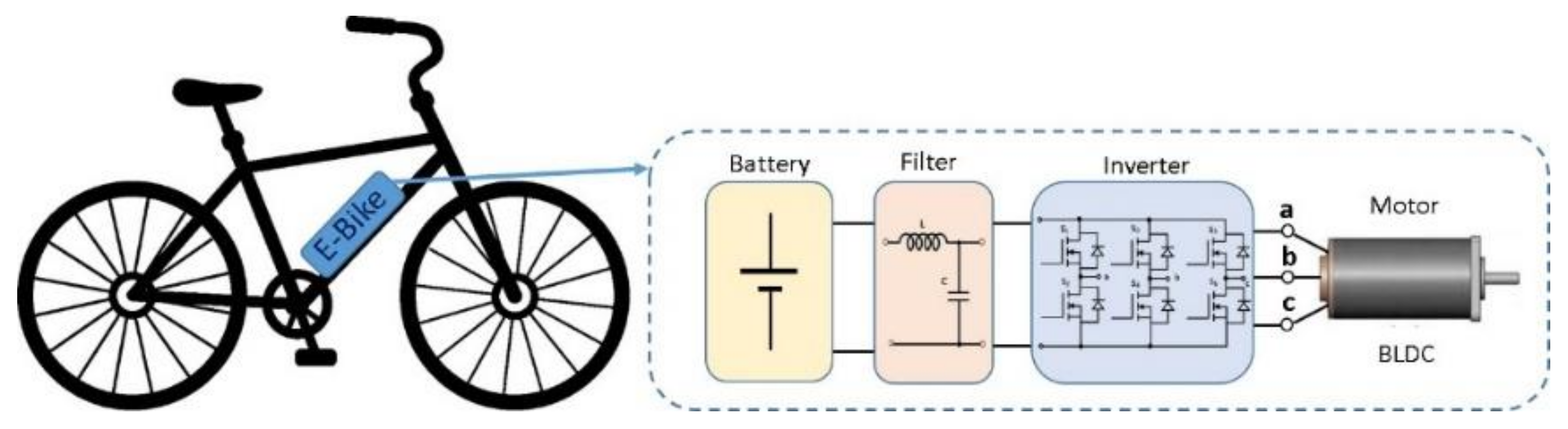
:1. Introduction
2. GaN FETs-Based Inverter Legs Power Stage
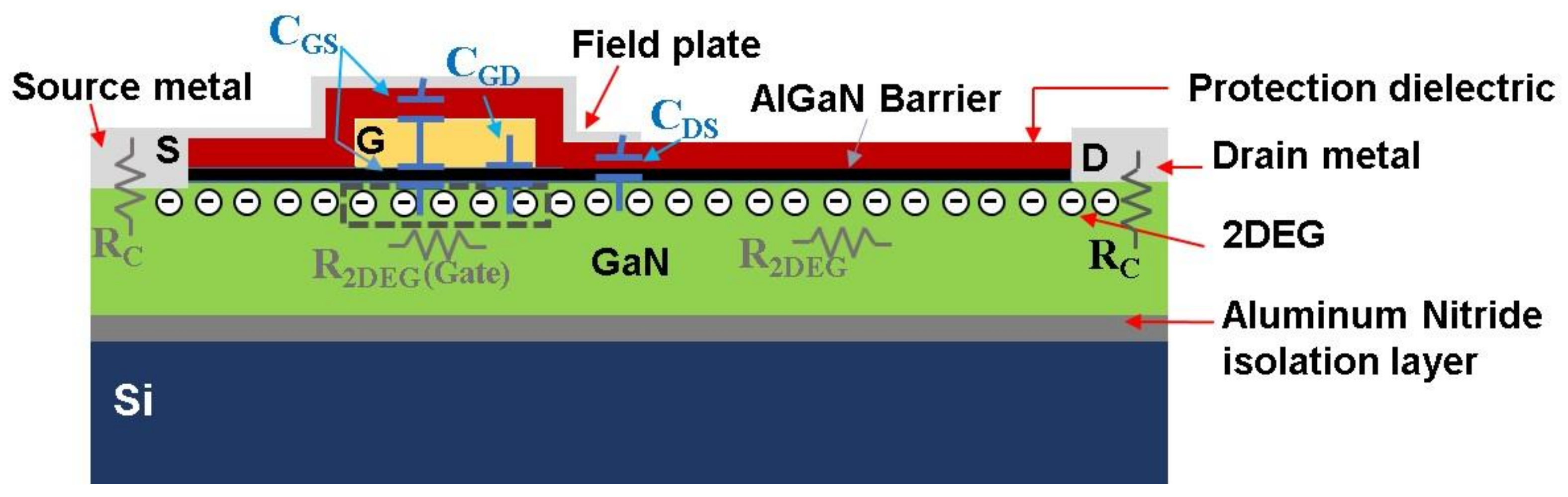
2.1. Low-Voltage GaN FETs Operation and Technology Survey
- gate threshold,
- conduct resistance and temperature behaviour,
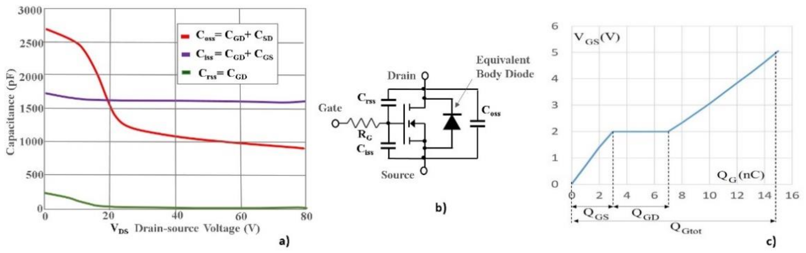
- structure parasitic capacitors,
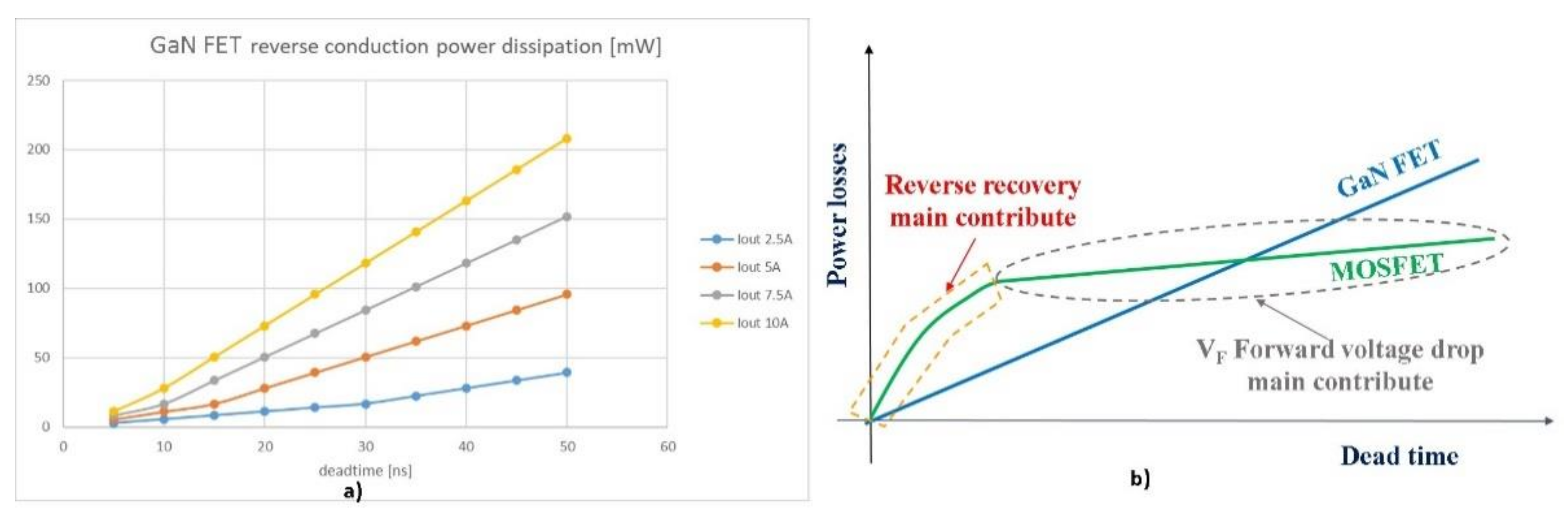
- reverse conduction mode.
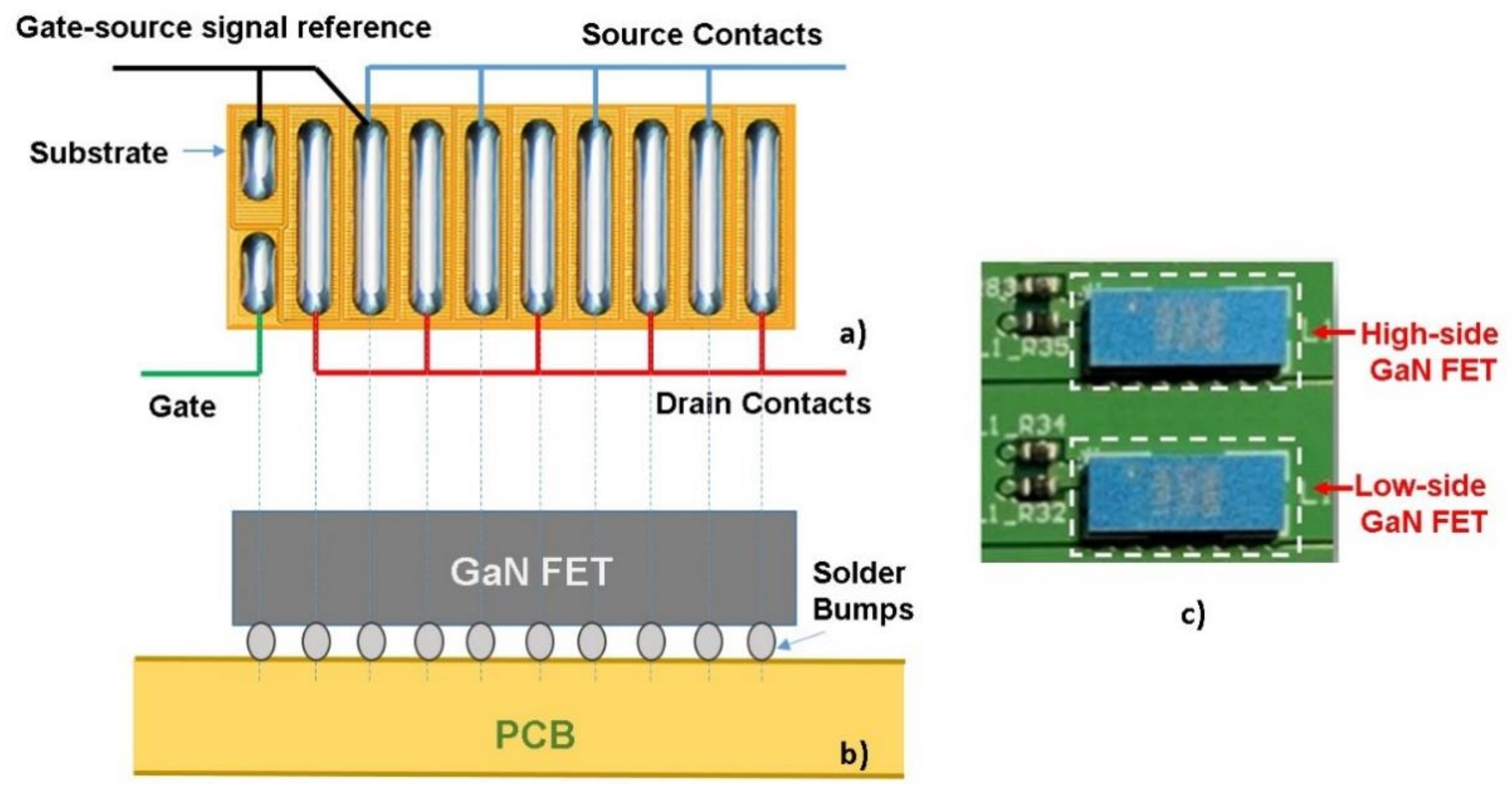
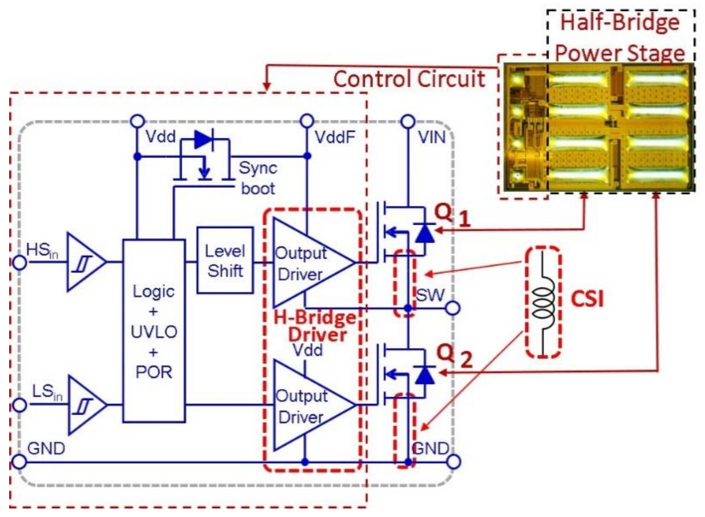
2.2. Packaging Issue and Integrating Solutions
Power Stage Integration
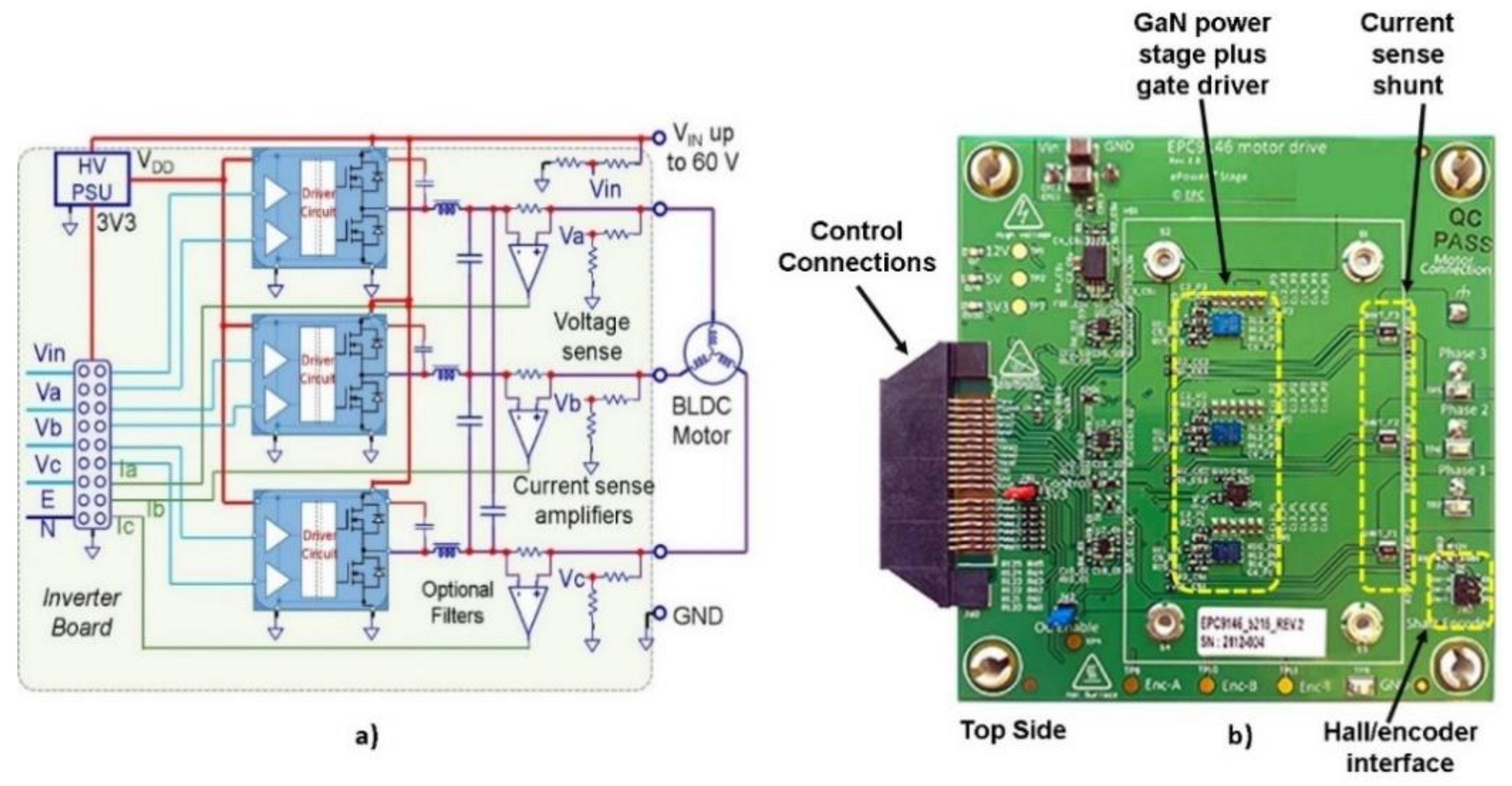
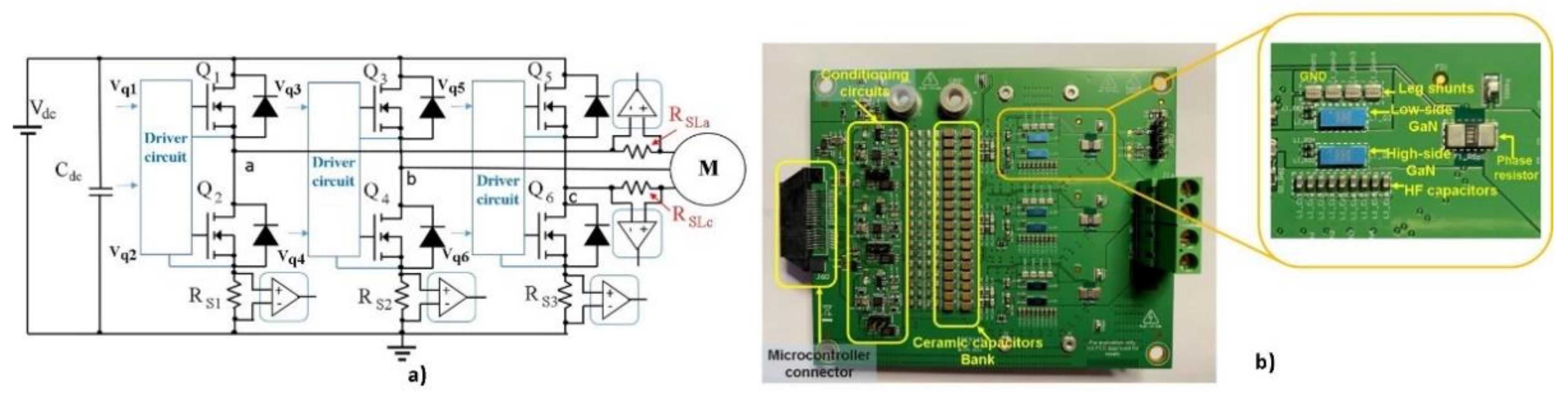
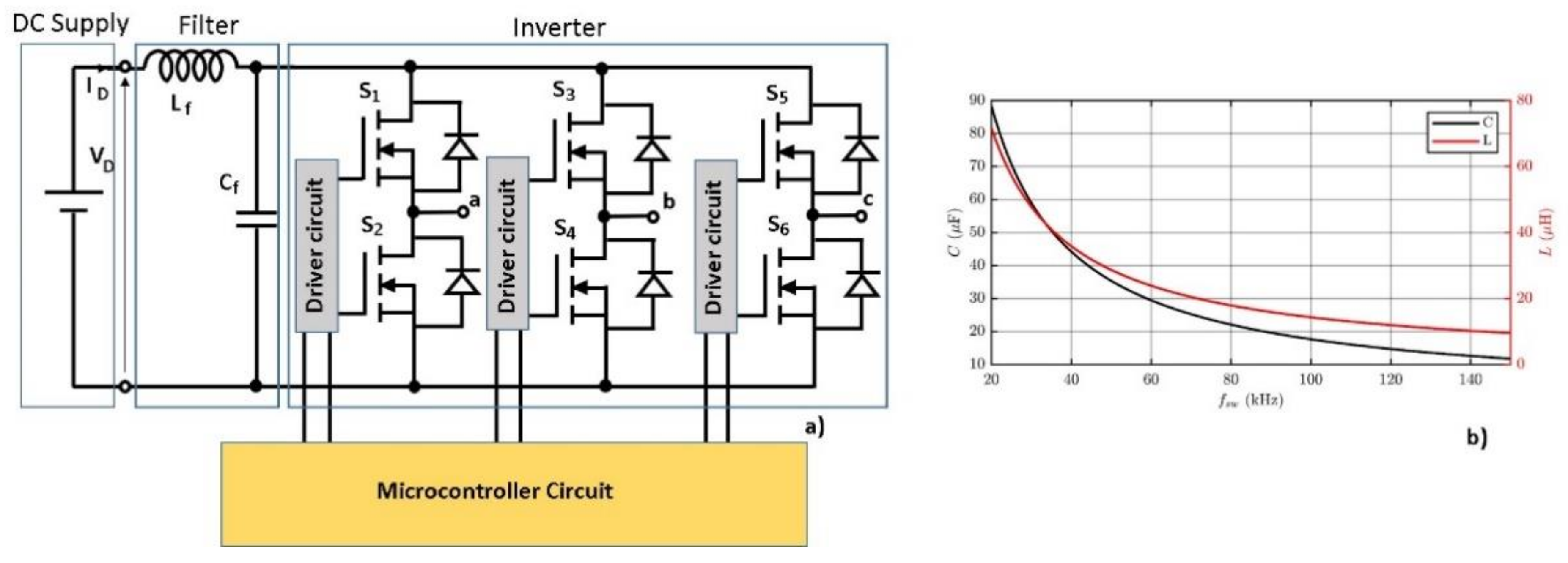
2.3. Inverter Circuit Arrangement
2.3.1. Notes on the Inverter Legs Layout
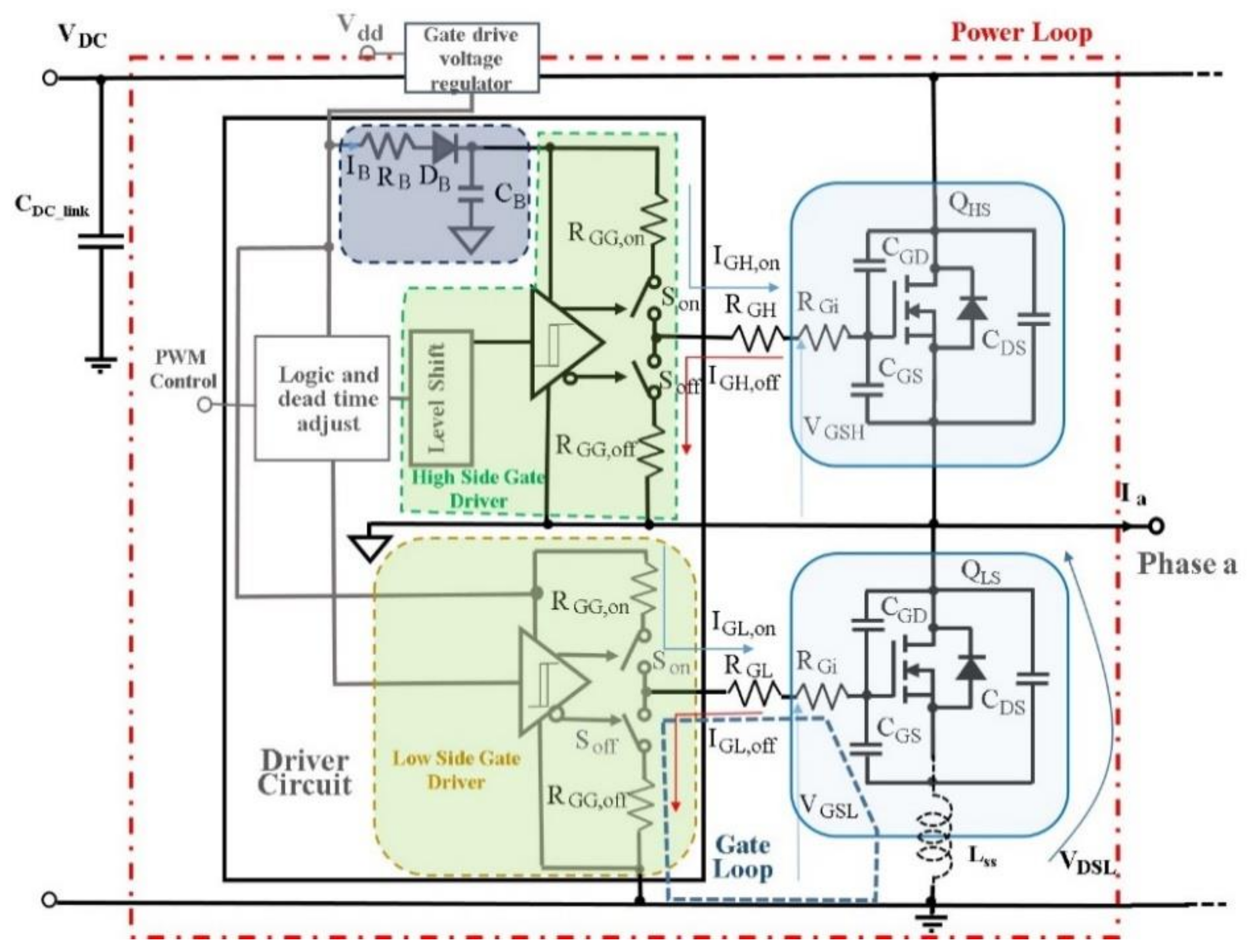
2.3.2. Driver Circuit Requirements
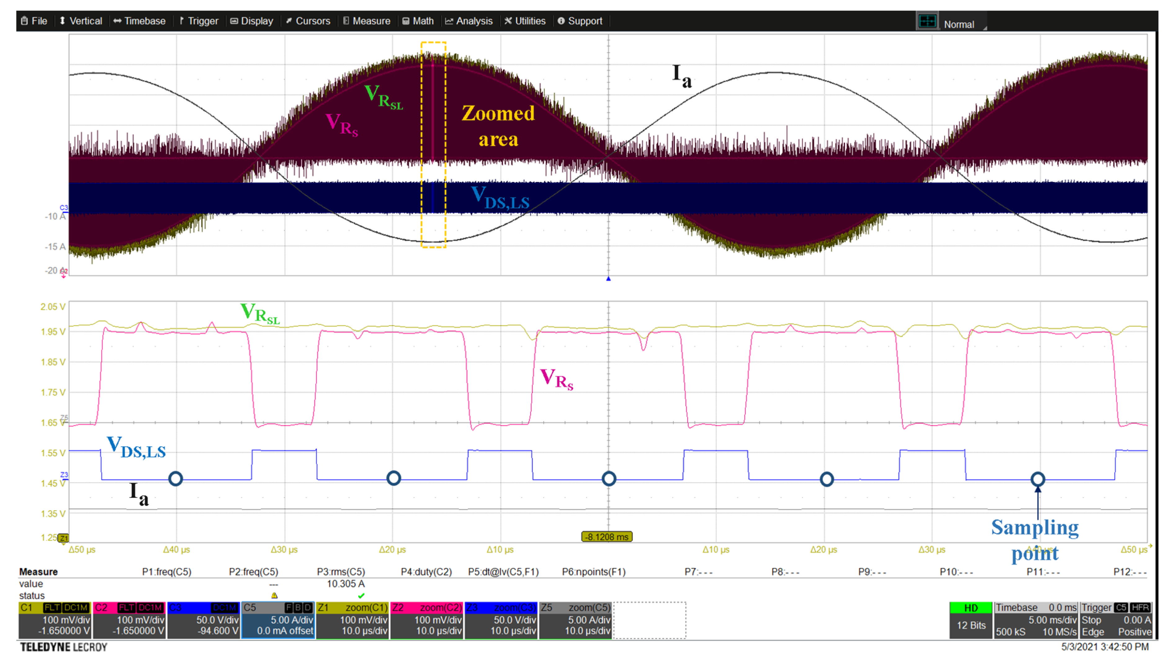
2.3.3. Current Sensing Arrangement
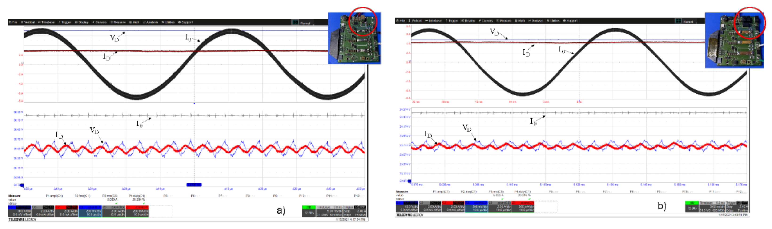
3. Input Current and Voltage Ripple Issues
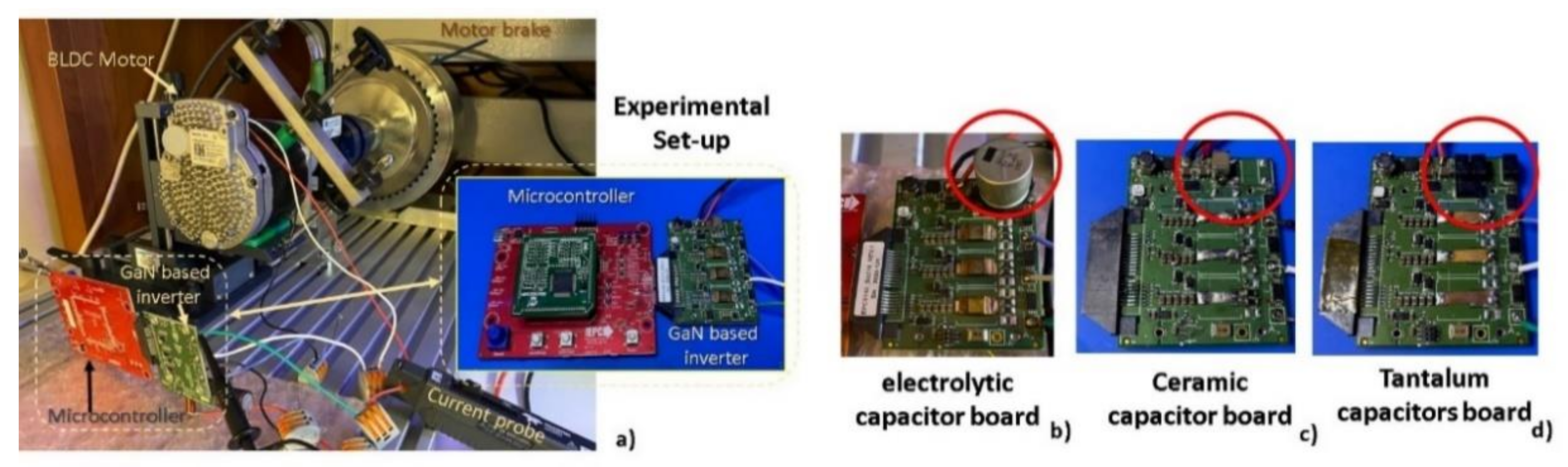
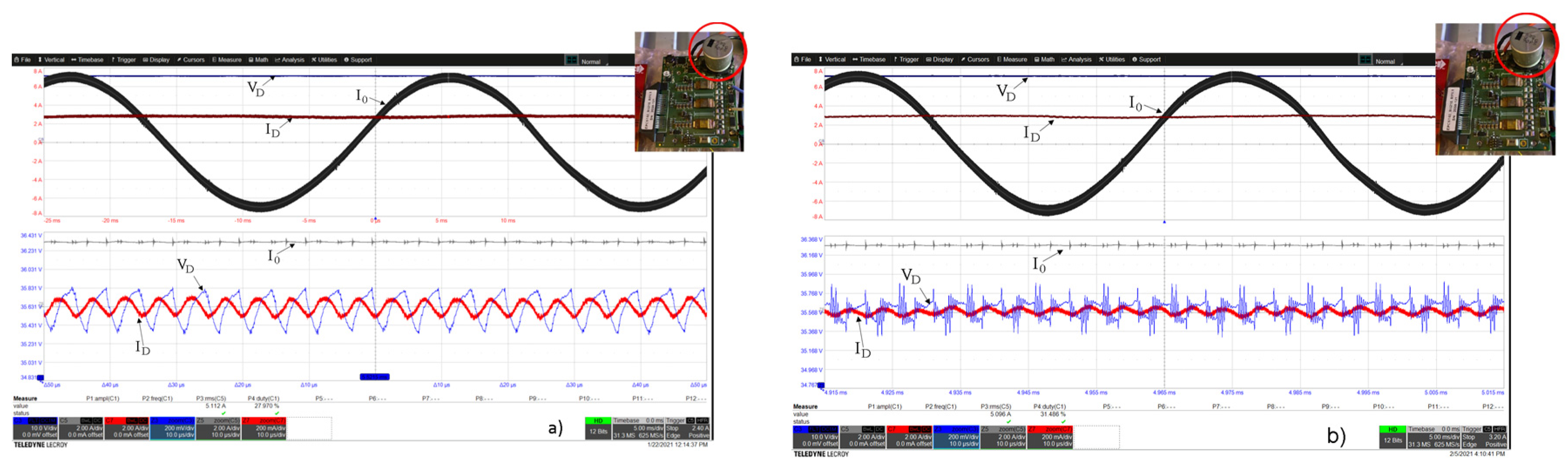
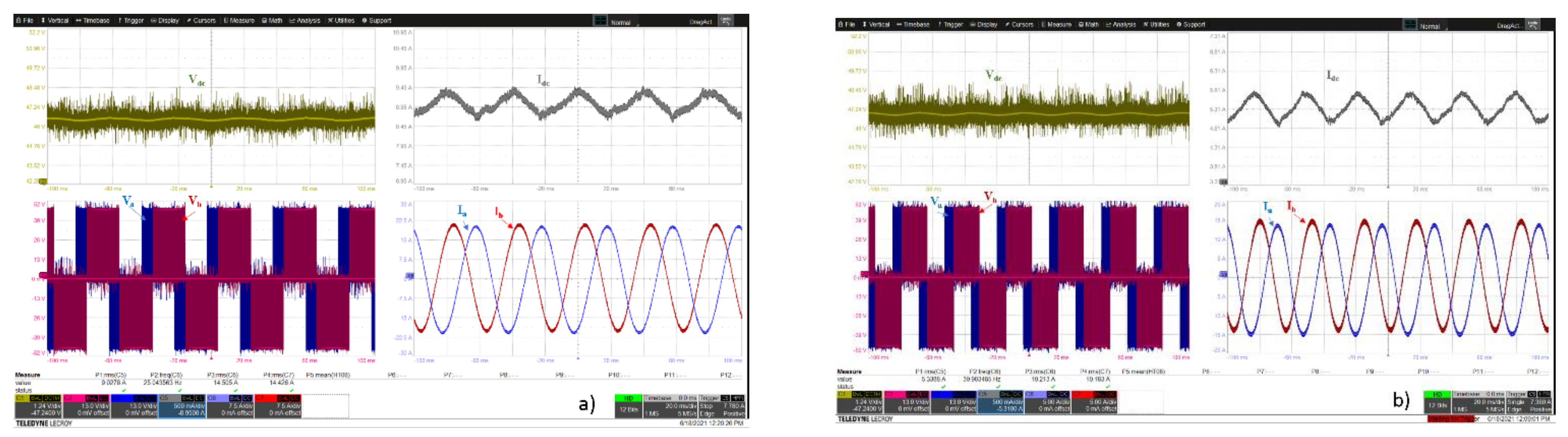
Experimental Evaluation of the Input Electrical Quantities Versus Switching Frequency Variation
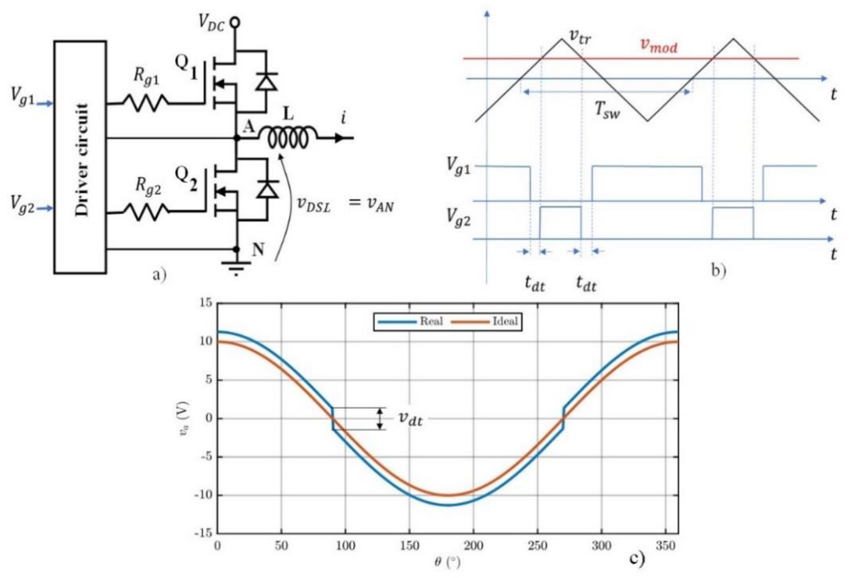
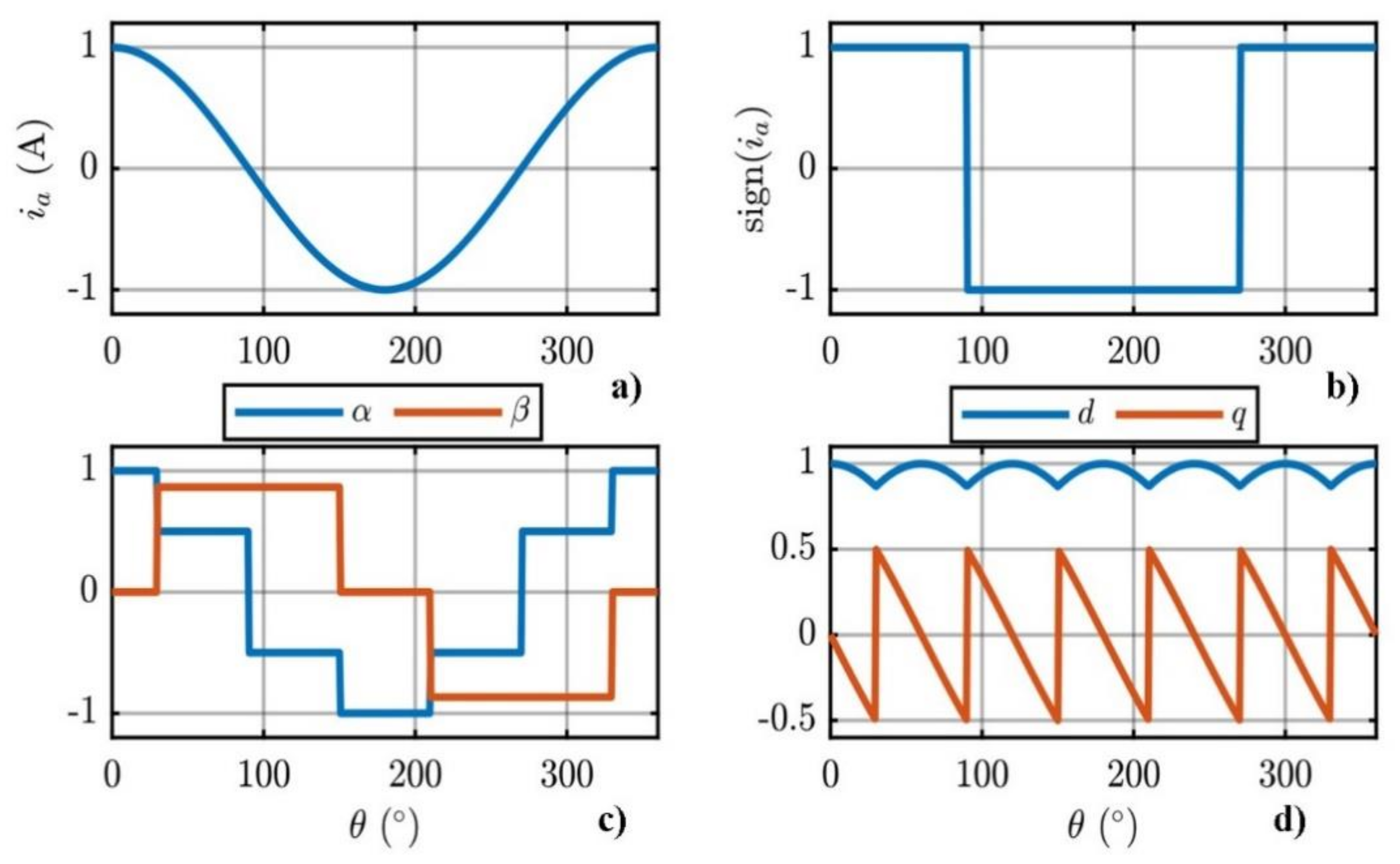
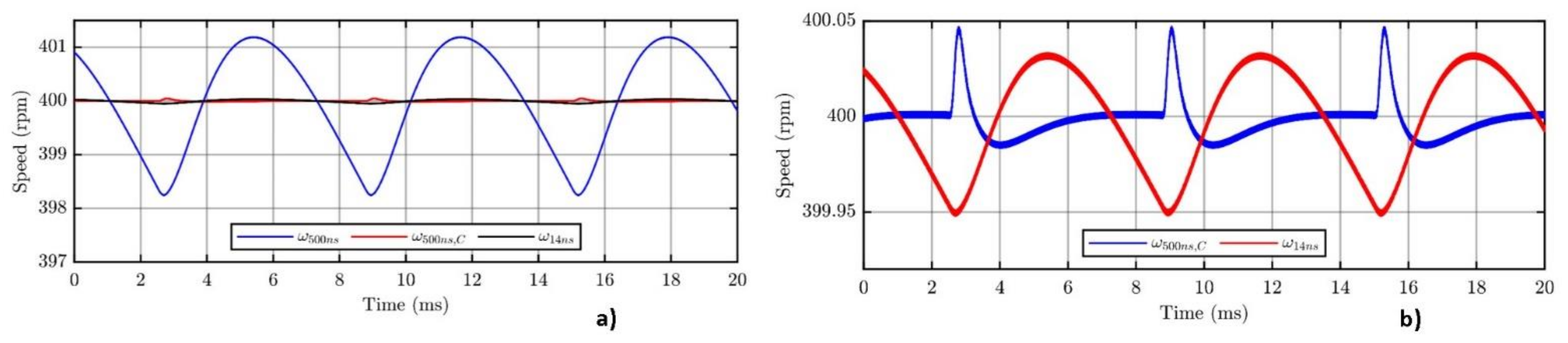
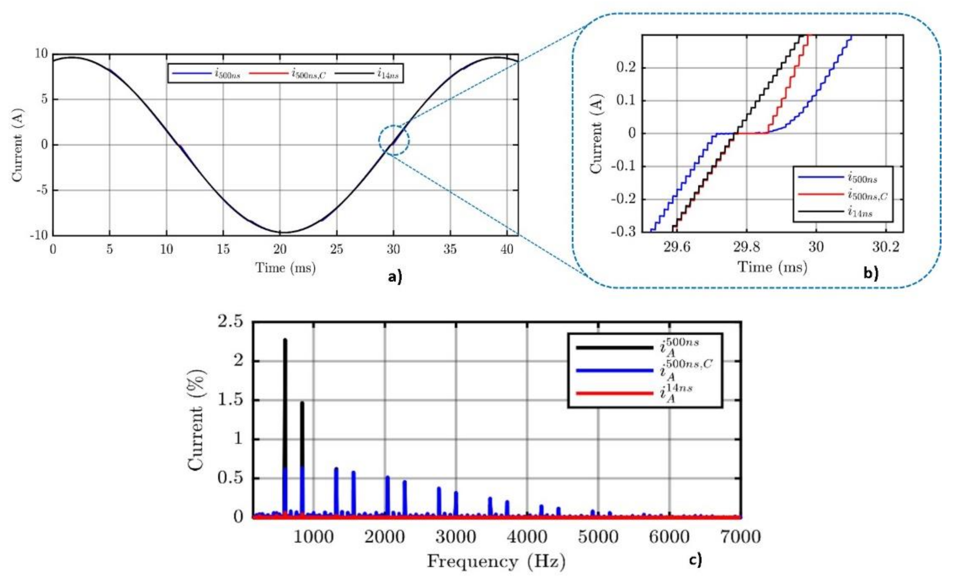
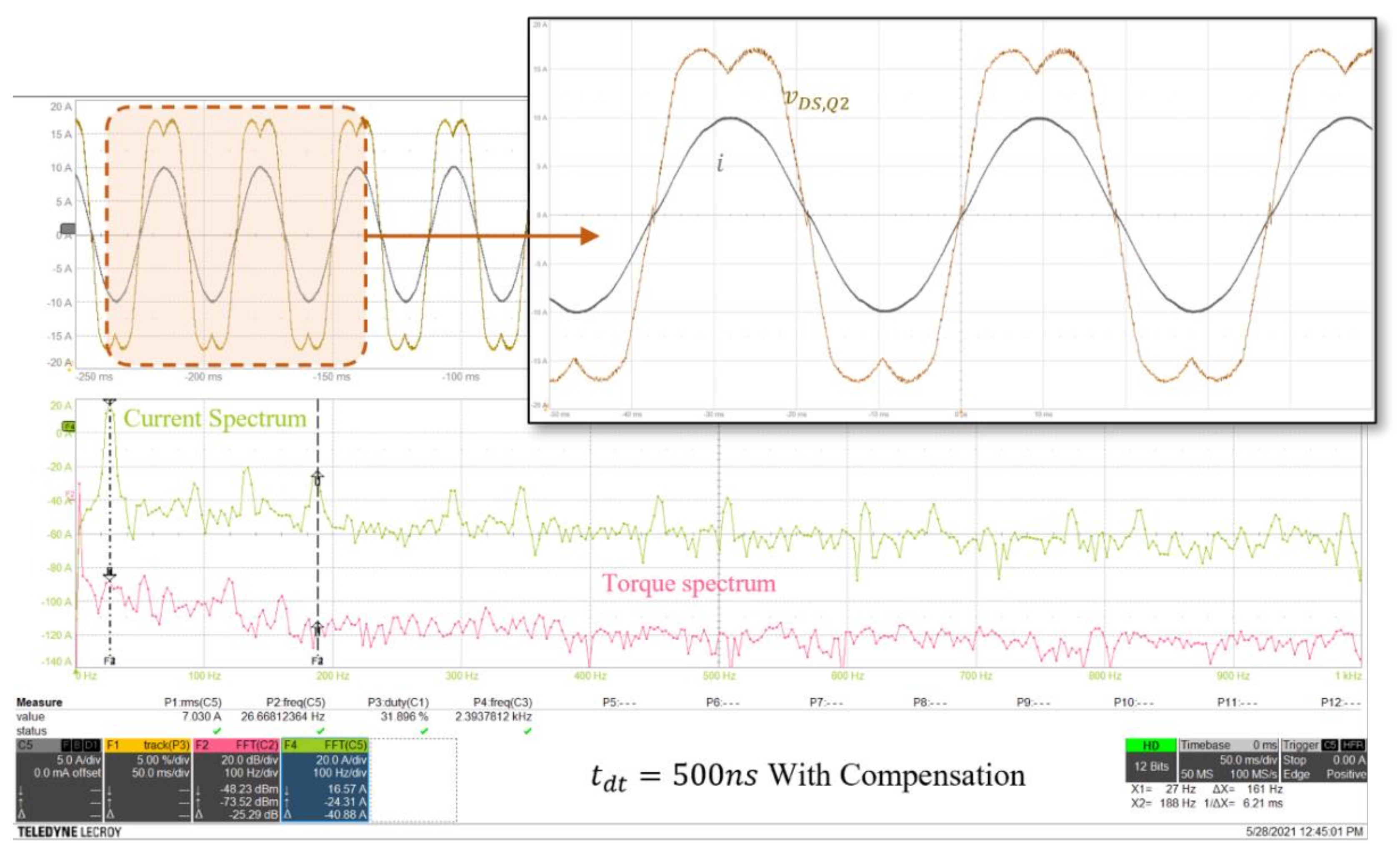
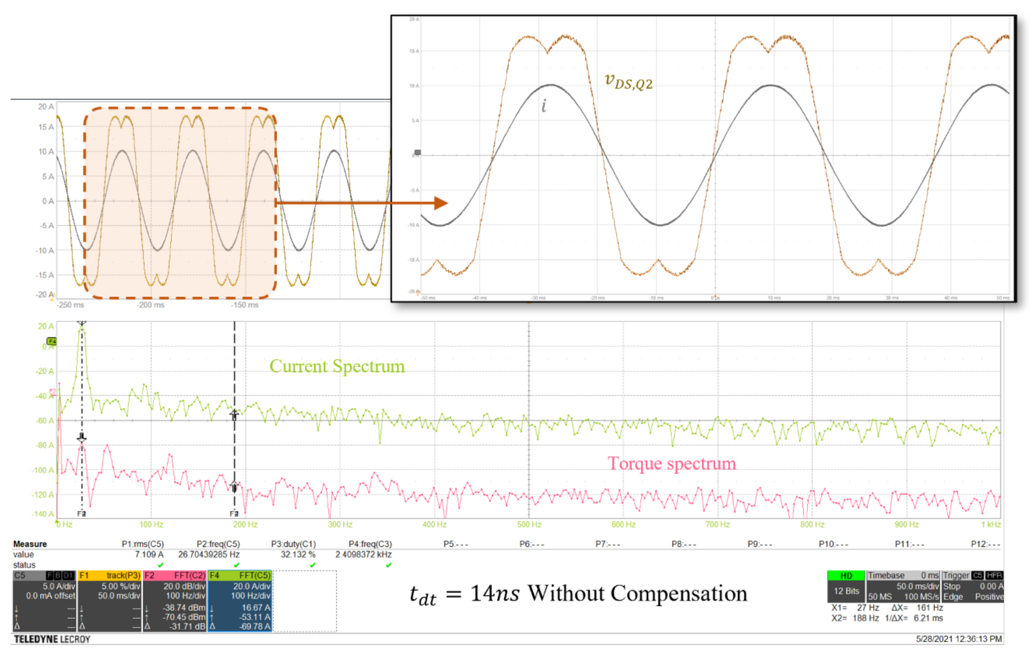
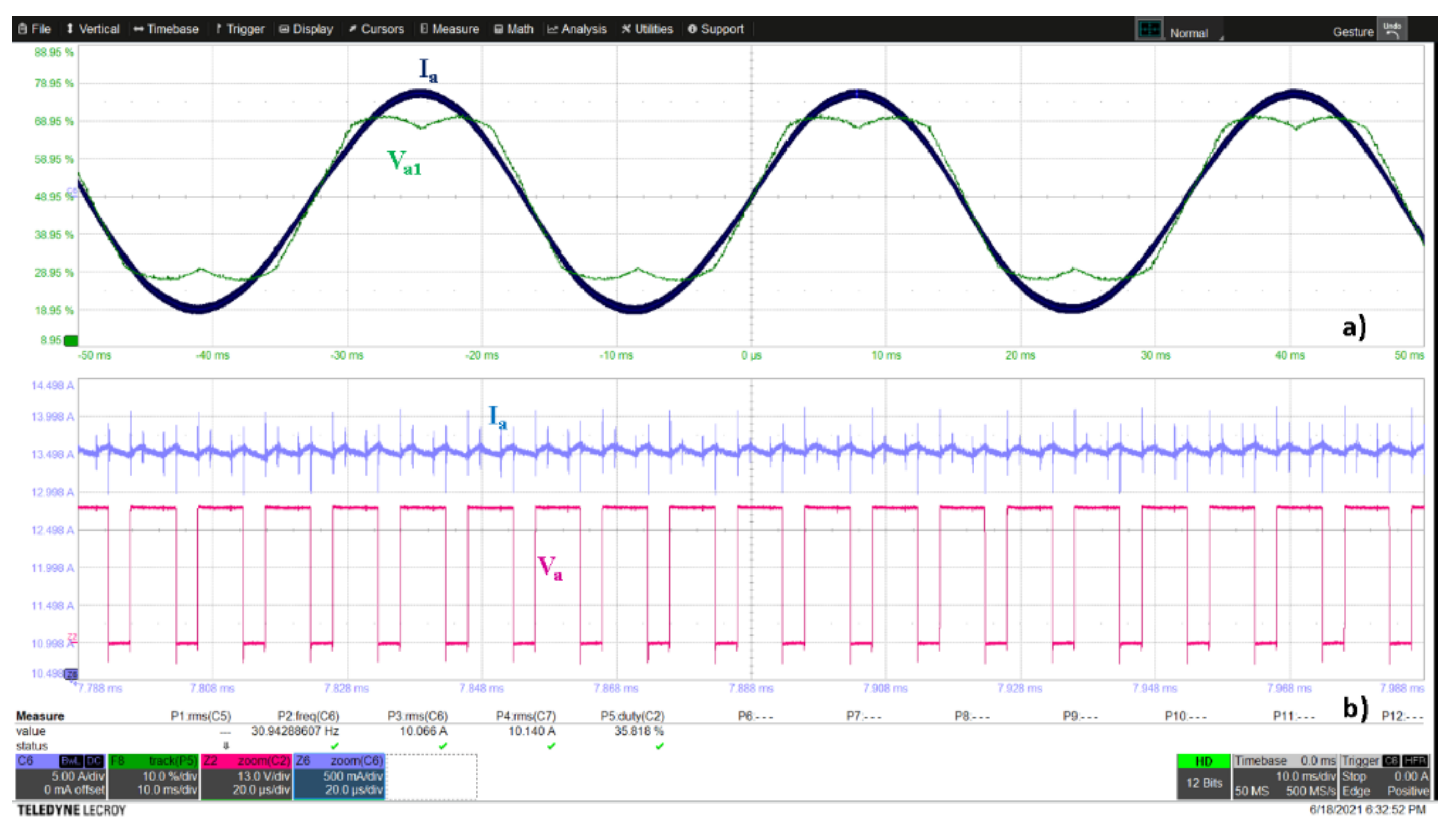
4. Dead Time Effect on the Motor Drives Inverters
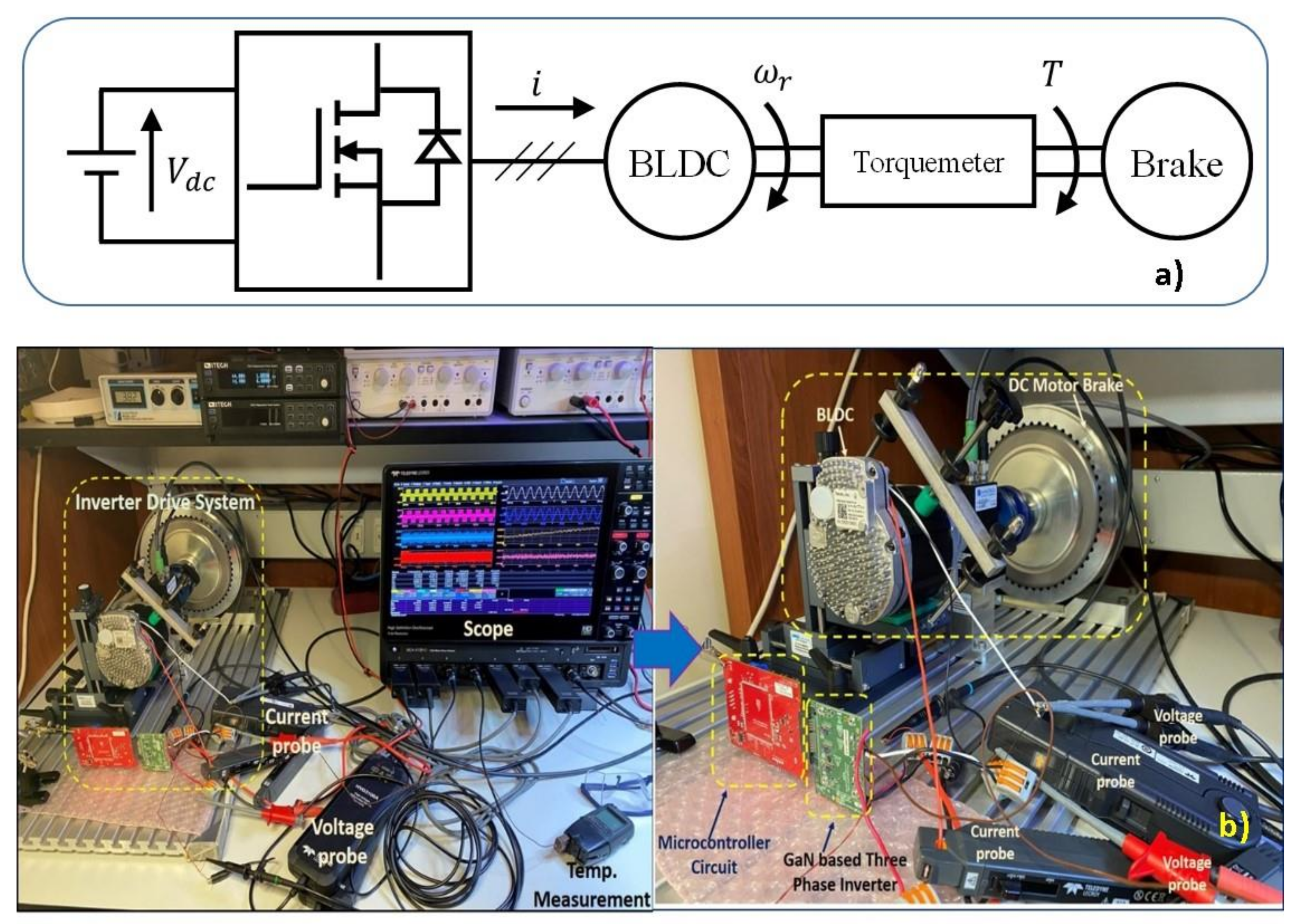
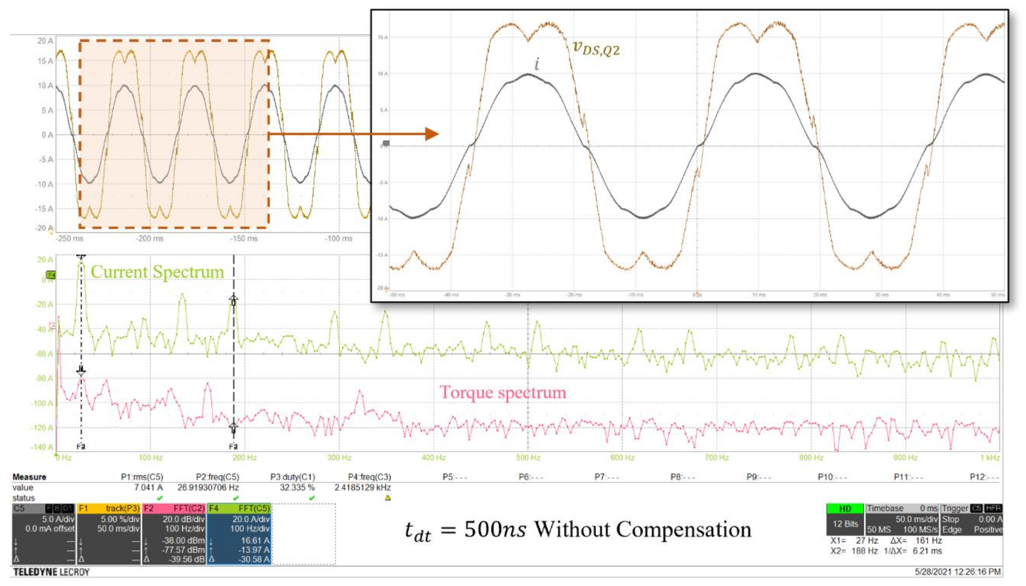
Simulation and Experimental Results
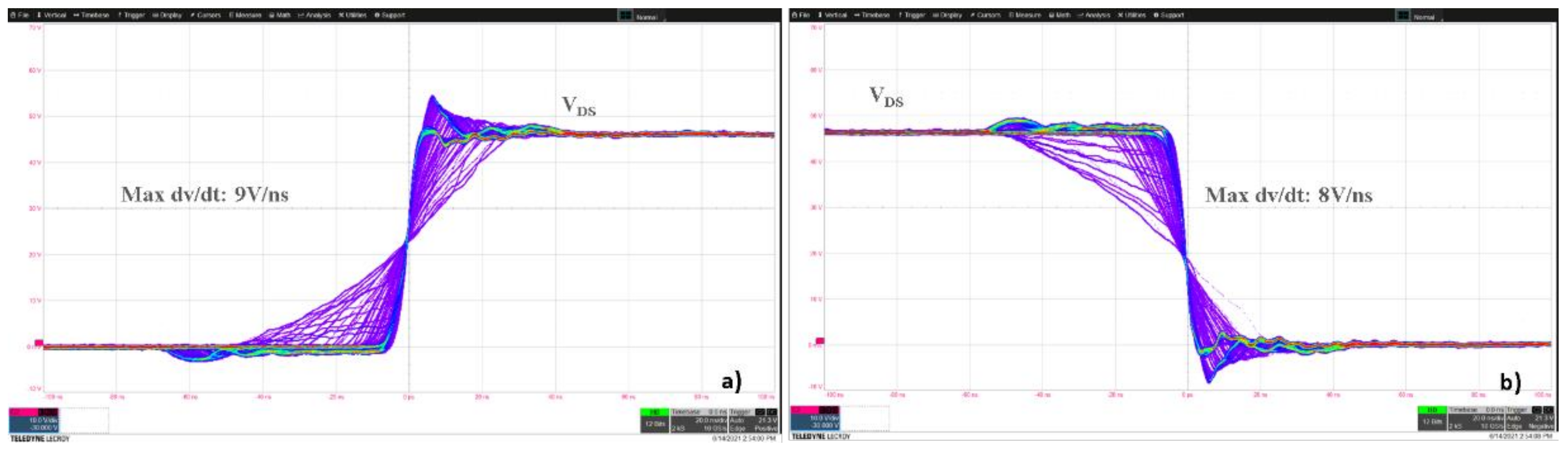
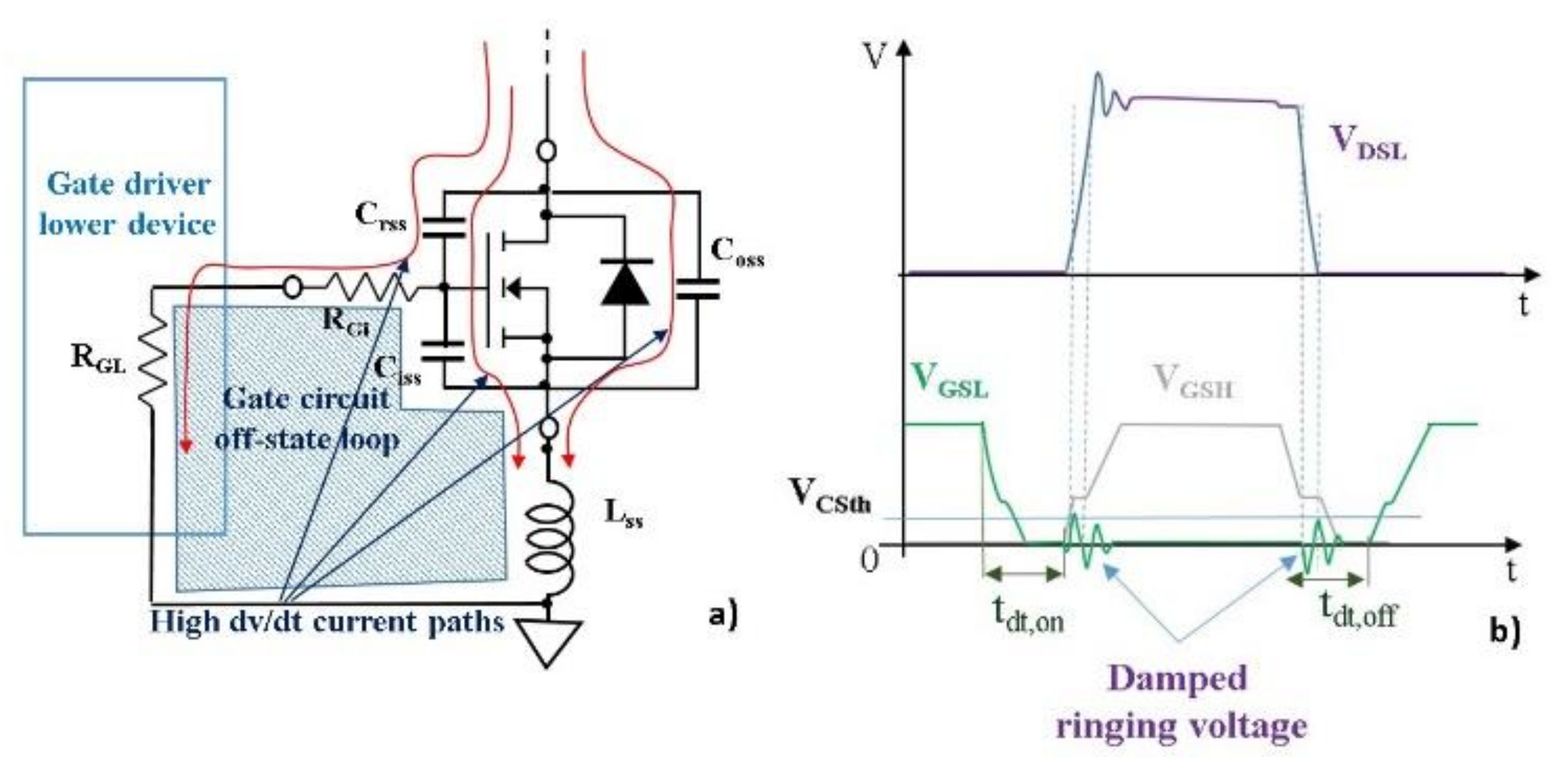
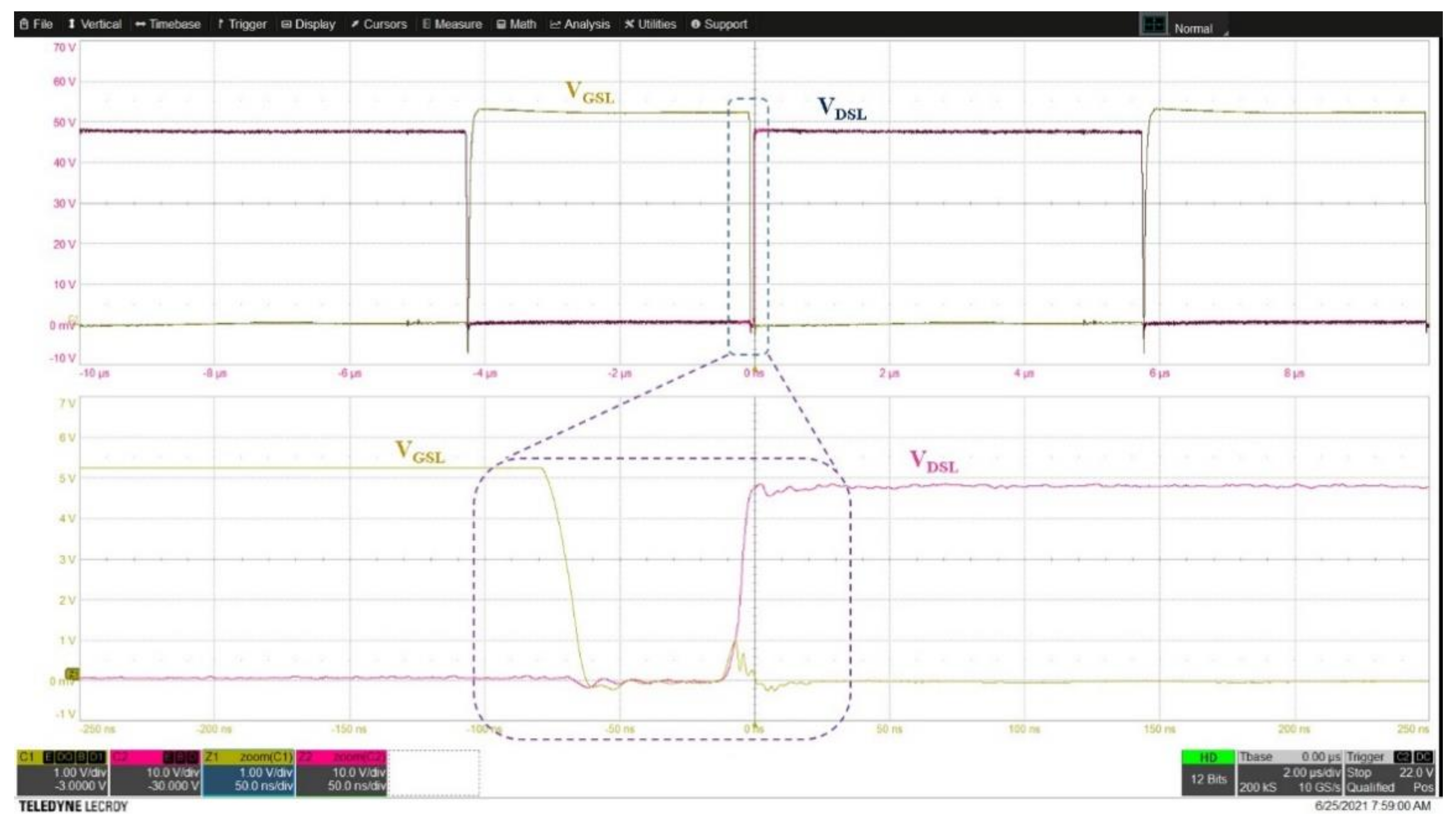
5. dv/dt Effect in the Switching Leg
6. Discrete GaN FET-Based Inverter Switching Evaluation
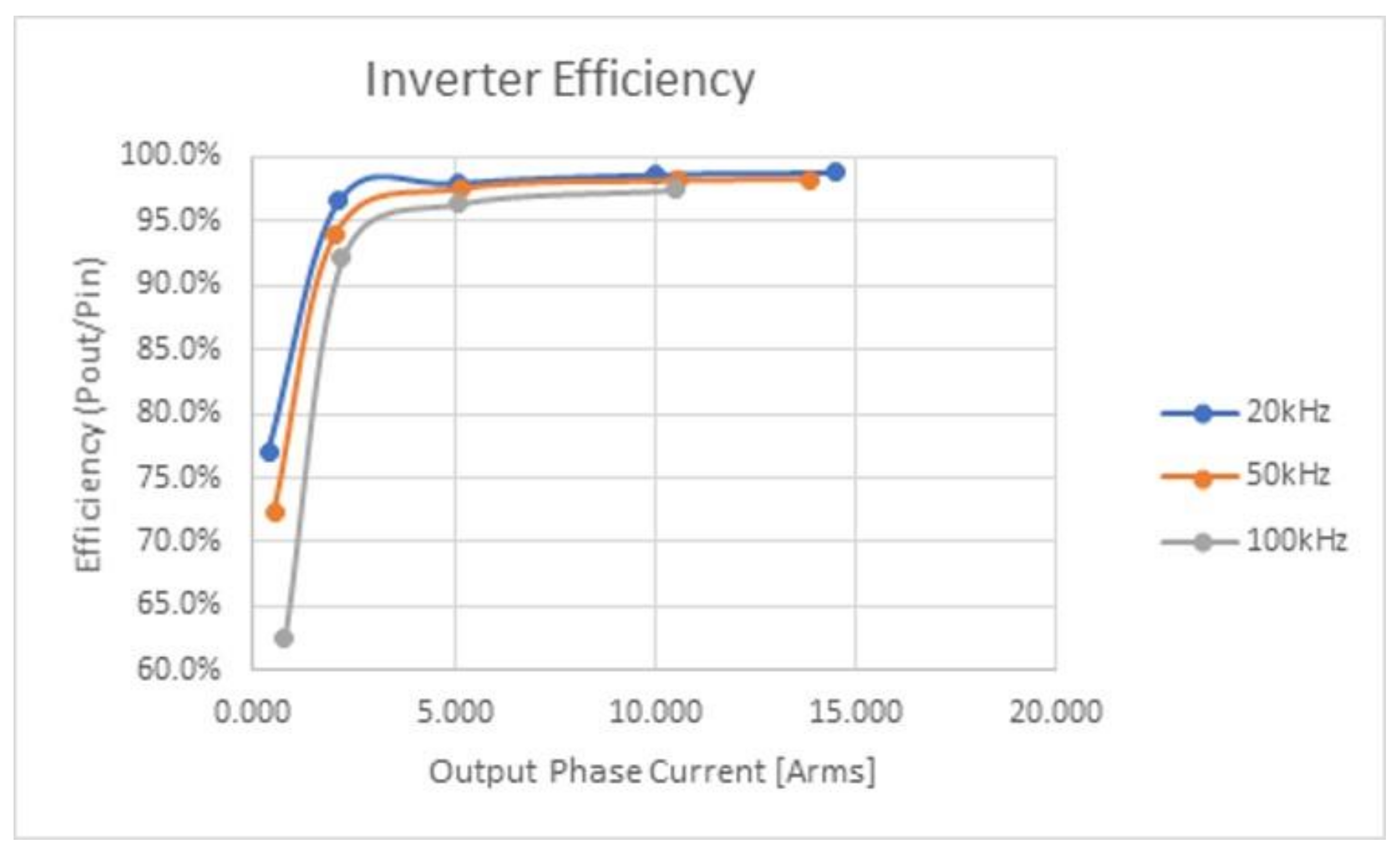
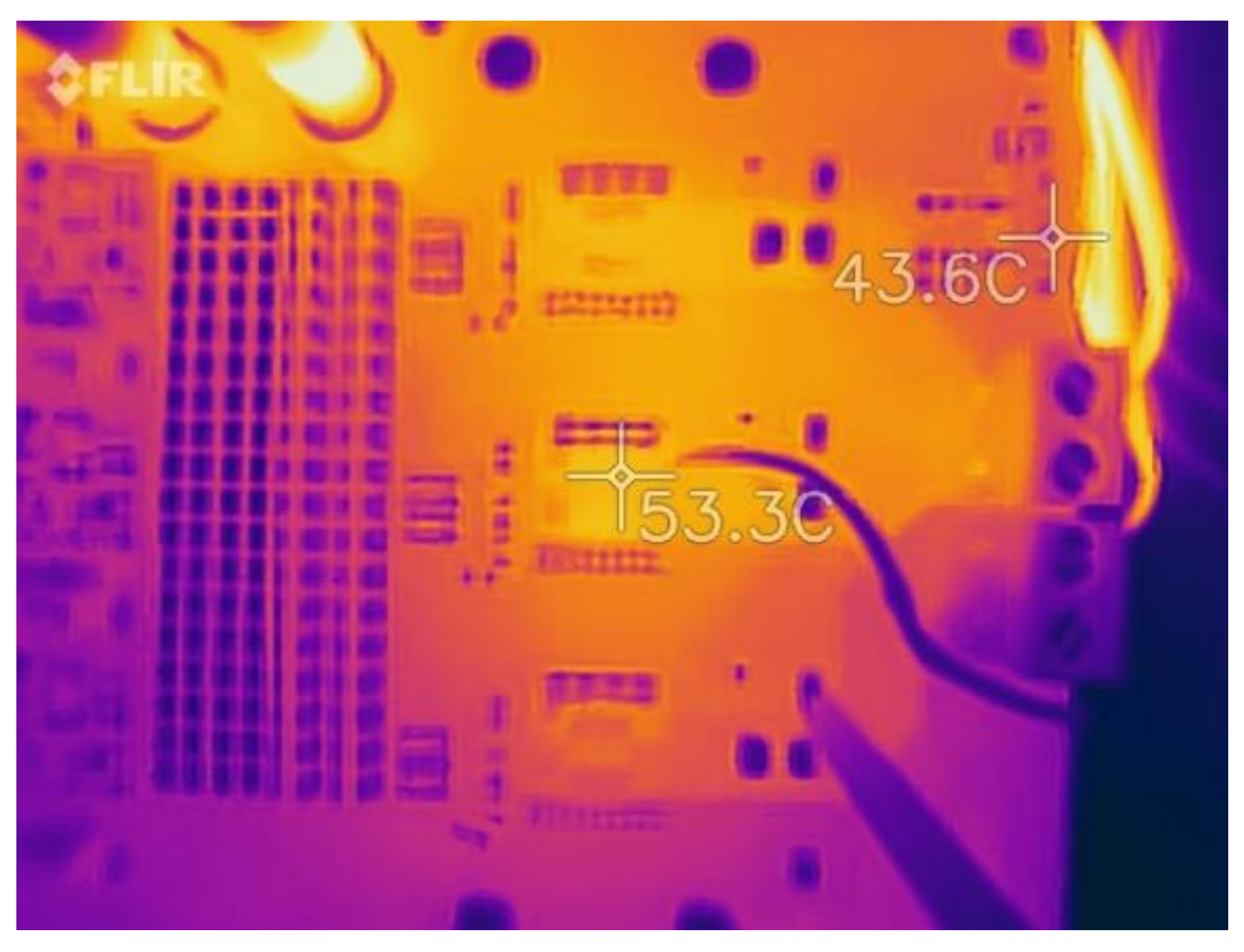
Thermal Behavior
7. Discussion
- –
- to the PCB at the board-side
- –
- to the case at the other side.
8. Conclusions
- quality of the current output waveforms
- torque obtained by reducing the harmonics and related oscillations
- total system efficiency.
Author Contributions
Funding
Institutional Review Board Statement
Informed Consent Statement
Data Availability Statement
Conflicts of Interest
Abbreviations
| GaN | Gallium Nitride |
| FET | Field Effect Transistor |
| HEMT | High Electron Mobility Transistors |
| WBG | Wide Bandgap |
| SiC | Silicon Carbide |
| Si | Silicon |
| UAV | Unmanned Aerial Vehicles |
| MOSFET | Metal Oxide Semiconductor Field Effect Transistor |
| IGBT | Insulated Gate Bipolar Transistor |
| EMI | Electromagnetic Interference |
| THD | Total Harmonic Distortion |
| IMMD | Integrated Modular Motor Drive |
| 2DEG | Two-Dimensional Electron Gas |
| AlGaN | Aluminum Gallium Nitride |
| FOM | Figure of Merit |
| EPC | Efficient Power Conversion |
| CSI | Common Source Inductance |
| PCB | Printed Circuit Board |
| CSP | Chip-Scale Package |
| UVLO | Voltage-Lockout |
| CMOS | Complementary MOS |
| TTL | Transistor-Transistor Logic |
| BLDC | Brushless DC |
| PWM | Pulse Width Modulation |
| PM | Permanent Magnetic |
| SMD | Surface Mounting Device |
| HSF | Hard Switching Fault |
| FUL | Fault Under Load |
| FOC | Field-Oriented Control |
| LS | Low Side |
| HS | High Side |
| CV | Capacitance/Voltage |
| ESR | Equivalent Series Resistance |
| ESL | Equivalent Series Inductance |
| PMAC | Permanent Magnetic AC |
References
- Wang, J.; Li, Y.; Han, Y. Integrated Modular Motor Drive Design With GaN Power FETs. IEEE Trans. Ind. Appl. 2015, 51, 3198–3207. [Google Scholar] [CrossRef]
- Musumeci, S.; Scrimizzi, F.; Fusillo, F.; Bojoi, R.; Longo, G.; Mistretta, C. Low Voltage High Current Trench-Gate MOSFET Inverter for Belt Starter Generator Applications. In Proceedings of the 2019 AEIT International Conference of Electrical and Electronic Technologies for Automotive (AEIT AUTOMOTIVE), Turin, Italy, 2–4 July 2019; pp. 1–6. [Google Scholar] [CrossRef]
- Faraci, G.; Raciti, A.; Rizzo, S.A.; Schembra, G. Green wireless power transfer system for a drone fleet managed by reinforcement learning in smart industry. Appl. Energy 2020, 259, 114204. [Google Scholar] [CrossRef]
- Wang, Y.; Liu, Y.-J.; Yu, C.-H.; Cao, F. A Novel Trench-Gated Power MOSFET With Reduced Gate Charge. IEEE Electron. Device Lett. 2014, 36, 165–167. [Google Scholar] [CrossRef]
- Armando, E. Low Voltage Trench-Gate MOSFETs for High Efficiency Auxiliary Power Supply Applications. In Proceedings of the 2019 International Conference on Clean Electrical Power (ICCEP), Otranto, Italy, 2–4 July 2019; pp. 165–170. [Google Scholar] [CrossRef]
- Wang, B.; Dong, S.; Jiang, S.; He, C.; Hu, J.; Ye, H.; Ding, X. A Comparative Study on the Switching Performance of GaN and Si Power Devices for Bipolar Complementary Modulated Converter Legs. Energies 2019, 12, 1146. [Google Scholar] [CrossRef] [Green Version]
- Ma, C.-T.; Gu, Z.-H. Review of GaN HEMT Applications in Power Converters over 500 W. Electronics 2019, 8, 1401. [Google Scholar] [CrossRef] [Green Version]
- De Rooij, M.; Perez, B.; Qiu, H.; Zhang, Y. A Low Voltage BLDC Motor Drive Inverter Using a Monolithic GaN ePowe(TM) Stage. In Proceedings of the PCIM Europe Digital Days 2020, International Exhibition and Conference for Power Electronics, Intelligent Motion, Renewable Energy and Energy Management, Nuremberg, Germany, 7–8 July 2020; pp. 1–7, ISBN 978-3-8007-5245-4. [Google Scholar]
- Kolar, J.; Round, S. Analytical calculation of the RMS current stress on the DC-link capacitor of voltage-PWM converter systems. IEE Proc. Electr. Power Appl. 2006, 153, 535–543. [Google Scholar] [CrossRef] [Green Version]
- Chierchie, F.; Paolini, E.; Stefanazzi, L. Dead-Time Distortion Shaping. IEEE Trans. Power Electron. 2018, 34, 53–63. [Google Scholar] [CrossRef]
- Zammit, D.; Staines, C.S.; Apap, M. Compensation techniques for non-linearities in H-bridge inverters. J. Electr. Syst. Inf. Technol. 2016, 3, 361–376. [Google Scholar] [CrossRef] [Green Version]
- Wang, L.; Qin, Z.; Dong, J.; Bauer, P. Design, modelling and evaluation of a GaN based motor drive for a solar car. In Proceedings of the IECON 2019—45th Annual Conference of the IEEE Industrial Electronics Society, Lisbon, Portugal, 14–17 October 2019; pp. 5120–5125. [Google Scholar] [CrossRef]
- Itoh, J.; Araki, T. Volume evaluation of a PWM inverter with wide band-gap devices for motor drive system. In Proceedings of the 2013 IEEE ECCE Asia Downunder, Melbourne, Australia, 3–6 June 2013; pp. 372–378. [Google Scholar] [CrossRef]
- Sun, B.; Burgos, R.; Boroyevich, D. Assessment of Switching Frequency Effect on a Compact Three-Phase GaN-Based Inverter Design. In Proceedings of the 2018 IEEE Energy Conversion Congress and Exposition (ECCE), Portland, OR, USA, 23–27 September 2018; pp. 868–875. [Google Scholar] [CrossRef]
- Salomez, F.; Vienot, S.; Zaidi, B.; Videt, A.; Duquesne, T.; Pichon, H.; Semail, E.; Idir, N. Design of an integrated GaN inverter into a multiphase PMSM. Proceeding of the 2020 IEEE Vehicle Power and Propulsion Conference (VPPC), Gijon, Spain, 18 November–16 December 2020; pp. 1–6. [Google Scholar] [CrossRef]
- Nifa, I.; Leroux, C.; Torres, A.; Charles, M.; Reimbold, G.; Ghibaudo, G.; Bano, E. Characterization and modeling of 2DEG mobility in AlGaN/AlN/GaN MIS-HEMT. Microelectron. Eng. 2019, 215, 110976. [Google Scholar] [CrossRef]
- Lidow, A.; De Rooij, M.; Strydom, J.; Reusch, D.; Glaser, J. GaN Transistors for Efficient Power Conversion, 3rd ed.; John Wiley & Sons: Hoboken, NJ, USA, 2019. [Google Scholar] [CrossRef]
- Raciti, A.; Musumeci, S.; Chimento, F.; Privitera, G. A new thermal model for power MOSFET devices accounting for the behavior in unclamped inductive switching. Microelectron. Reliab. 2016, 58, 3–11. [Google Scholar] [CrossRef]
- Bojoi, R.; Fusillo, F.; Raciti, A.; Musumeci, S.; Scrimizzi, F.; Rizzo, S. Full-Bridge DC-DC Power Converter for Telecom applications with Advanced Trench Gate MOSFETs. In Proceedings of the 2018 IEEE International Telecommunications Energy Conference (INTELEC), Turin, Italy, 7–11 October 2018; pp. 1–7. [Google Scholar] [CrossRef]
- McArthur, V. Making Use of Gate Charge Information in MOSFET and IGBT Data Sheets. Advanced Power Technology, Application Note. 2001. Available online: https://www.microsemi.com/document-portal/doc_view/14697-making-use-of-gate-charge-information-in-mosfet-and-igbt-data-sheets (accessed on 5 October 2021).
- Sorensen, C.; Fogsgaard, M.L.; Christiansen, M.N.; Graungaard, M.K.; Norgaard, J.B.; Uhrenfeldt, C.; Trintis, I. Conduction, reverse conduction and switching characteristics of GaN E-HEMT. In Proceedings of the 2015 IEEE 6th International Symposium on Power Electronics for Distributed Generation Systems (PEDG), Aachen, Germany, 22–25 June 2015; pp. 1–7. [Google Scholar] [CrossRef]
- Fichtenbaum, N.; Giandalia, M.; Sharma, S.; Zhang, J. Half-Bridge GaN Power ICs: Performance and Application. IEEE Power Electron. Mag. 2017, 4, 33–40. [Google Scholar] [CrossRef]
- Musumeci, S.; Panizza, M.; Stella, F.; Perraud, F. Monolithic Bidirectional Switch Based on GaN Gate Injection Transistors. In Proceedings of the 2020 IEEE 29th International Symposium on Industrial Electronics (ISIE), Delft, The Netherlands, 17–19 June 2020; pp. 1045–1050. [Google Scholar] [CrossRef]
- EPC9146—Development Board. Available online: https://epc-co.com/epc/Products/DemoBoards/EPC9146.aspx (accessed on 5 October 2021).
- Sun, B.; Jorgensen, K.L.; Zhang, Z.; Andersen, M.A. Research of Power Loop Layout and Parasitic Inductance in GaN Transistor Implementation. IEEE Trans. Ind. Appl. 2021, 57, 1677–1687. [Google Scholar] [CrossRef]
- Ming, X.; Zhang, Z.; Fan, Z.; Qin, Y.; Liu, Y.; Zhang, B. High Reliability GaN FET Gate Drivers for Next-generation Power Electronics Technology. In Proceedings of the 2019 IEEE 13th International Conference on ASIC (ASICON), Chongqing, China, 29 October–1 November 2019; pp. 1–4. [Google Scholar] [CrossRef]
- Santra, S.B.; Roy, A.; Chatterjee, D. Design of Bootstrap Capacitor Based GaN-FET driver for Improvement in Transient Performance of DC-DC Converter. In Proceedings of the 2020 IEEE International Conference on Power Electronics, Smart Grid and Renewable Energy (PESGRE2020), Cochin, India, 2–4 January 2020; pp. 1–6. [Google Scholar] [CrossRef]
- Musumeci, S.; Pagano, R.; Raciti, A.; Frisina, F.; Melito, M. Transient behavior of IGBTs submitted to fault under load conditions. In Proceedings of the 2002 IEEE Industry Applications Conference, 37th IAS Annual Meeting (Cat. No.02CH37344), Pittsburgh, PA, USA, 13–18 October 2002; Volume 3, pp. 2182–2189. [Google Scholar] [CrossRef]
- Vujacic, M.; Hammami, M.; Srndovic, M.; Grandi, G. Analysis of dc-Link Voltage Switching Ripple in Three-Phase PWM Inverters. Energies 2018, 11, 471. [Google Scholar] [CrossRef] [Green Version]
- Moradpour, M.; Serpi, A.; Gatto, G. Dead-Time Analysis of a Universal SiC-GaN-Based DC-DC Converter for Plug-In Electric Vehicles. In Proceedings of the IECON 2018—44th Annual Conference of the IEEE Industrial Electronics Society, Washington, DC, USA, 21–23 October 2018; pp. 1134–1139. [Google Scholar] [CrossRef]
- Di Mauro, S.; Musumeci, S.; Raciti, A.; Fusillo, F.; Scrimizzi, F.; Scollo, R. Synchronous rectification with low voltage MOSFETs in LLC converters. In Proceedings of the 2017 AEIT International Annual Conference, Cagliari, Italy, 20–22 September 2017; pp. 1–6. [Google Scholar] [CrossRef]
- Glaser, J.S.; Reusch, D. Comparison of deadtime effects on the performance of DC-DC converters with GaN FETs and silicon MOSFETs. In Proceedings of the 2016 IEEE Energy Conversion Congress and Exposition (ECCE), Milwaukee, WI, USA, 18–22 September 2016; pp. 1–8. [Google Scholar] [CrossRef]
- Holtz, J.; Quan, J. Sensorless vector control of induction motors at very low speed using a nonlinear inverter model and parameter identification. IEEE Trans. Ind. Appl. 2002, 38, 1087–1095. [Google Scholar] [CrossRef]
- Bojoi, I.R.; Armando, E.; Pellegrino, G.; Rosu, S. Self-commissioning of inverter nonlinear effects in AC drives. In Proceedings of the 2012 IEEE International Energy Conference and Exhibition (ENERGYCON), Florence, Italy, 9–12 September 2012; pp. 213–218. [Google Scholar]
- Pellegrino, G.; Guglielmi, P.; Armando, E.G.; Bojoi, I.R. Self-Commissioning Algorithm for Inverter Nonlinearity Compensation in Sensorless Induction Motor Drives. IEEE Trans. Ind. Appl. 2010, 46, 1416–1424. [Google Scholar] [CrossRef] [Green Version]
- Hwang, S.-H.; Kim, J.-M. Dead Time Compensation Method for Voltage-Fed PWM Inverter. IEEE Trans. Energy Convers. 2010, 25, 1–10. [Google Scholar] [CrossRef]
- Urasaki, N.; Senjyu, T.; Uezato, K.; Funabashi, T. An Adaptive Dead-Time Compensation Strategy for Voltage Source Inverter Fed Motor Drives. IEEE Trans. Power Electron. 2005, 20, 1150–1160. [Google Scholar] [CrossRef]
- Munoz, A.R.; Lipo, T.A. On-line dead-time compensation technique for open-loop PWM-VSI drives. IEEE Trans. Power Electron. 1999, 14, 683–689. [Google Scholar] [CrossRef] [Green Version]
- De Doncker, R.W.; Veltman, A.; Pulle, D.W.J. Advanced Electrical Drives: Analysis, Modeling, Control; Springer: Dordrecht, The Netherlands, 2011; ISBN 978-94-007-0179-3. [Google Scholar]
- Mandrile, F.; Musumeci, S.; Palma, M. Dead Time Management in GaN Based Three-Phase Motor Drives. In Proceedings of the 23rd European Conference on Power Electronics and Applications, EPE’21 ECCE Europe, Ghent, Belgium, 6–10 September 2021; pp. 1–10, in press. [Google Scholar]
- Caruso, M.; Di Tommaso, A.O.; Miceli, R.; Nevoloso, C.; Vassallo, G.; Vitamia, G. FOC with Resolver Implementation for PMSM Drives by Using a Low Cost Atmel SAM3X8E Microcontroller. In Proceedings of the 2020 Fifteenth International Conference on Ecological Vehicles and Renewable Energies (EVER), Monte-Carlo, Monaco, 10–12 September 2020; pp. 1–8. [Google Scholar] [CrossRef]
- Cheng, S.; Chou, P.-C. Investigation on the parallel operation of All-GaN power module and thermal performance evaluation. In Proceedings of the 2014 International Power Electronics Conference (IPEC-Hiroshima 2014—ECCE ASIA), Hiroshima, Japan, 18–21 May 2014; pp. 3425–3431. [Google Scholar] [CrossRef]
- Chimento, F.; Raciti, A.; Cannone, A.; Musumeci, S.; Gaito, A. Parallel connection of super-junction MOSFETs in a PFC application. In Proceedings of the 2009 IEEE Energy Conversion Congress and Exposition, San Jose, CA, USA, 20–24 September 2009; pp. 3776–3783. [Google Scholar] [CrossRef]
- Shi, Y.; Chen, W.; Cui, X.; Li, M.; Liu, C.; Xia, Y.; Li, J.; Wang, F.; Xin, Y.; Zhou, Q.; et al. Investigation on the Long-Term Reliability of High-Voltage p-GaN HEMT by Repetitively Transient Overcurrent. IEEE Trans. Electron. Devices 2018, 65, 5322–5328. [Google Scholar] [CrossRef]
- Rizzo, S.A.; Susinni, G.; Iannuzzo, F. Intrusiveness of Power Device Condition Monitoring Methods: Introducing Figures of Merit for Condition Monitoring. IEEE Ind. Electron. Mag. 2021. [Google Scholar] [CrossRef]
- Palma, M.; Musumeci, S.; Mandrile, F.; Barba, V. GaN Devices for Motor Drive Applications. In Proceedings of the 8th IEEE Workshop on Wide Bandgap Power Devices and Applications (WiPDA 2021), Fully Virtual Workshop, Redondo Beach, CA, USA, 7–9 November 2021. in press. [Google Scholar]
- Efthymiou, L.; Camuso, G.; Longobardi, G.; Chien, T.; Chen, M.; Udrea, F. On the Source of Oscillatory Behaviour during Switching of Power Enhancement Mode GaN HEMTs. Energies 2017, 10, 407. [Google Scholar] [CrossRef]
- Pastura, M.; Nuzzo, S.; Kohler, M.; Barater, D. Dv/Dt Filtering Techniques for Electric Drives: Review and Challenges. In Proceedings of the IECON 2019—45th Annual Conference of the IEEE Industrial Electronics Society, Lisbon, Portugal, 14–17 October 2019; pp. 7088–7093. [Google Scholar] [CrossRef] [Green Version]
- Abdullah, Y.; Petrdikakis, W.; Li, H.; Wang, K.; Zhang, Y.; Wang, X.; Wang, J.; Liu, L.; Bala, S. A Hybrid PWM Modulation for EMI Filter Size Reduction in a 10 kW GaN-Based Three Phase Inverter. In Proceedings of the 2019 IEEE Applied Power Electronics Conference and Exposition (APEC), Anaheim, CA, USA, 17–21 March 2019; pp. 1897–1903. [Google Scholar] [CrossRef]
- Won, Y.; Cho, J.; Agonafer, D.; Asheghi, M.; Goodson, K.E. Fundamental Cooling Limits for High Power Density Gallium Nitride Electronics. IEEE Trans. Compon. Packag. Manuf. Technol. 2015, 5, 737–744. [Google Scholar] [CrossRef]
- Thermal Management of eGaN® FETs Application Note. Available online: https://epc-co.com/epc/Portals/0/epc/documents/application-notes/How2AppNote012%20-%20How%20to%20Get%20More%20Power%20Out%20of%20an%20eGaN%20Converter.pdf (accessed on 5 October 2021).
- Raciti, A.; Musumeci, S.; Cristaldi, D. Modeling and simulation of IGBT thermal behavior during a short circuit power pulse. In Proceedings of the 2015 International Conference on Clean Electrical Power (ICCEP), Taormina, Italy, 16–18 June 2015; pp. 542–547. [Google Scholar] [CrossRef]
- Wu, H.; Fayyaz, A.; Castellazzi, A. P-gate GaN HEMT gate-driver design for joint optimization of switching performance, freewheeling conduction and short-circuit robustness. In Proceedings of the 2018 IEEE 30th International Symposium on Power Semiconductor Devices and ICs (ISPSD), Chicago, IL, USA, 13–17 May 2018; pp. 232–235. [Google Scholar] [CrossRef]
- EPC eGaN® FETs Reliability Testing: Phase 11. Reliability Report. Available online: https://epc-co.com/epc/Portals/0/epc/documents/product-training/Reliability%20Report%20Phase%2011.pdf (accessed on 5 October 2021).
- Lyu, X.; Li, H.; Abdullah, Y.; Wang, K.; Hu, B.; Yang, Z.; Wang, J.; Liu, L.; Bala, S. A Reliable Ultra-Fast Three Step Short Circuit Protection Method for E-mode GaN HEMTs. In Proceedings of the 2019 IEEE Applied Power Electronics Conference and Exposition (APEC), Anaheim, CA, USA, 17–21 March 2019; pp. 437–440. [Google Scholar] [CrossRef]


| PMAC MOTOR | Motor Voltage Range Vm [V] | Nominal Rms Current Im [A] | Angular Speed Max ωmx [rpm] |
|---|---|---|---|
| 24–75 | 10 | 3010 |
| GaN Inverter | Bus Voltage Vdc [V] | Switching Frequency fsw [kHz] | Dead Time [ns] |
|---|---|---|---|
| 20 | |||
| 48 | 50 | 50 | |
| 100 |
Publisher’s Note: MDPI stays neutral with regard to jurisdictional claims in published maps and institutional affiliations. |
© 2021 by the authors. Licensee MDPI, Basel, Switzerland. This article is an open access article distributed under the terms and conditions of the Creative Commons Attribution (CC BY) license (https://creativecommons.org/licenses/by/4.0/).
Share and Cite
Musumeci, S.; Mandrile, F.; Barba, V.; Palma, M. Low-Voltage GaN FETs in Motor Control Application; Issues and Advantages: A Review. Energies 2021, 14, 6378. https://doi.org/10.3390/en14196378
Musumeci S, Mandrile F, Barba V, Palma M. Low-Voltage GaN FETs in Motor Control Application; Issues and Advantages: A Review. Energies. 2021; 14(19):6378. https://doi.org/10.3390/en14196378
Chicago/Turabian StyleMusumeci, Salvatore, Fabio Mandrile, Vincenzo Barba, and Marco Palma. 2021. "Low-Voltage GaN FETs in Motor Control Application; Issues and Advantages: A Review" Energies 14, no. 19: 6378. https://doi.org/10.3390/en14196378