
A Novel Buck Converter with Constant Frequency Controlled Technique


Abstract
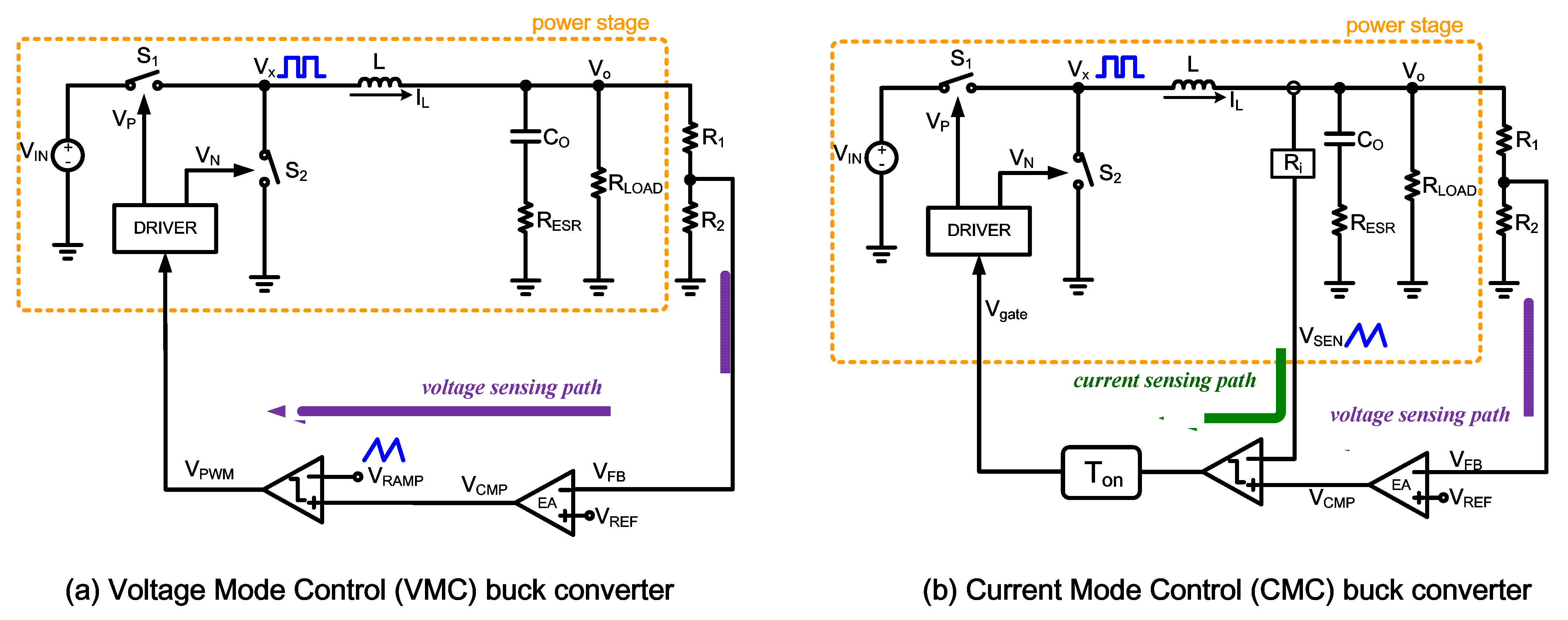
:1. Introduction
2. Conventional Control Schemes Descriptions
2.1. Conventional COT/AOT Control Scheme
2.2. Conventional AOT Scheme with PLL
3. Proposed Control Scheme and Frequency Detector
3.1. Proposed Control Scheme and Operating Principle
3.2. Proposed Frequency Detector
3.3. Proposed AOT
4. Design Procedure
4.1. Mathematical Modeling for Main Body Converter
4.2. Compensation Network Design for A(s)
4.3. Stability Analysis of Mathematical Model
- Step 1
- Step 2
- As expressed in (4), the zero . Using Equation (2), suppose can be obtained. In order to obtain a better output regulation, the A(s) gain is set to at least 60 dB. Thus, Ω, then gm = 100 μA/V, and 160 Hz. Finally, the values of gm, Ro, C1, and R1 are substituted into Equation (2).
- Step 3
- We substitute Equation (2) into Equation (3) and draw the Bode diagram of T(s) with MathCAD. Here, in Equation (3), the k is substituted by 0.5. The Bode diagrams of T(s), Gp(s), and A(s) are drawn in Figure 15. As can be seen from Figure 15, the T(s) phase margin is about 40 degrees, DC gain is about 71 dB, and the crossover frequency is about 400 kHz.
5. Simulation Results
5.1. SIMPLIS Schematic Building
5.2. Stability Analisis with SIMPLIS
5.3. Transient Performance
5.4. Load Regulation/Line Regulation
5.5. Switching Frquency Regulation
5.6. Performance List
6. Conclusions
Author Contributions
Funding
Data Availability Statement
Conflicts of Interest
References
- Chen, J.-J.; Lu, M.-X.; Wu, T.-H.; Hwang, Y.-S. Sub-1-V Fast-Response Hysteresis-Controlled CMOS Buck Converter Using Adaptive Ramp Techniques. IEEE Trans. Very Large Scale Integr. (VLSI) Syst. 2013, 21, 1608–1618. [Google Scholar] [CrossRef]
- Chen, J.-J.; Hwang, Y.-S.; Chen, J.-H.; Ku, Y.-T.; Yu, C.-C. A New Fast-Response Current-Mode Buck Converter with Improved I2-Controlled Techniques. IEEE Trans. Very Large Scale Integr. (VLSI) Syst. 2018, 26, 903–911. [Google Scholar] [CrossRef]
- Hwang, Y.S.; Chen, J.J.; Ku, Y.T.; Yang, J.Y. An Improved Optimum-Damping Current-Mode Buck Converter with Fast-Transient Response and Small-Transient Voltage using New Current Sensing Circuits. IEEE Trans. Ind. Electron. 2020, 68, 9505–9514. [Google Scholar] [CrossRef]
- Kim, M.; Kim, J. A PWM/PFM Dual-Mode DC-DC Buck Converter with Load-Dependent Efficiency-Controllable Scheme for Multi-Purpose IoT Applications. Energies 2021, 14, 960. [Google Scholar] [CrossRef]
- Nguyen, M.-K. Power Converters in Power Electronics: Current Research Trends. Electronics 2020, 9, 654. [Google Scholar] [CrossRef]
- Huang, Q.; Zhan, C.; Burm, J. A 30-MHz Voltage-Mode Buck Converter Using Delay-Line-Based PWM Control. IEEE Trans. Circuits Syst. II Express Briefs 2017, 65, 1659–1663. [Google Scholar] [CrossRef]
- Chen, J.-J.; Hwang, Y.-S.; Ku, Y.-T.; Li, Y.-H.; Chen, J.-A. A Current-Mode-Hysteretic Buck Converter with Constant-Frequency-Controlled and New Active-Current-Sensing Techniques. IEEE Trans. Power Electron. 2021, 36, 3126–3134. [Google Scholar] [CrossRef]
- Yan, Y.; Lee, F.C.; Mattavelli, P.; Liu, P.-H. I2 Average Current Mode Control for Switching Converters. IEEE Trans. Power Electron. 2014, 29, 2027–2036. [Google Scholar] [CrossRef]
- Redl, R.; Sokal, N.O. Current-mode control, five different types, used with the three basic classes of power converters: Small-signal AC and large-signal DC characterization, stability requirements, and implementation of practical circuits. In Proceedings of the 1985 IEEE Power Electronics Specialists Conference, Toulouse, France, 24–28 June 1985; pp. 771–785. [Google Scholar]
- Li, J. Current-Mode Control: Modeling and its Digital Application. Ph.D. Dissertation, Virginia Polytechnic Institute and State University, Blacksburg, VA, USA, 2009. [Google Scholar]
- Zhong, S.; Shen, Z. A Hybrid Constant On-Time Mode for Buck Circuits. Electronics 2021, 10, 930. [Google Scholar] [CrossRef]
- Lin, Y.-C.; Chen, C.-J.; Chen, D.; Wang, B. A Ripple-Based Constant On-Time Control With Virtual Inductor Current and Offset Cancellation for DC Power Converters. IEEE Trans. Power Electron. 2012, 27, 4301–4310. [Google Scholar] [CrossRef]
- Nien, C.-F.; Chen, D.; Hsiao, S.-F.; Kong, L.; Chen, C.-J.; Chan, W.-H.; Lin, Y.-L. A Novel Adaptive Quasi-Constant On-Time Current-Mode Buck Converter. IEEE Trans. Power Electron. 2017, 32, 8124–8133. [Google Scholar] [CrossRef]
- Lin, H.-C.; Fung, B.-C.; Chang, T.-Y. A current mode adaptive on-time control scheme for fast transient DC-DC converters. In Proceedings of the 2008 IEEE International Symposium on Circuits and Systems, Seattle, WA, USA, 18–21 May 2008; pp. 2602–2605. [Google Scholar]
- Zhen, S.; Zhou, S.; Zeng, L.; Yang, M.; Ming, X.; Luo, P.; Zhang, B. Variable on time controlled buck converter for DVS applications. In Proceedings of the IECON 2017—43rd Annual Conference of the IEEE Industrial Electronics Society, Beijing, China, 29 October–1 November 2017; pp. 1642–1648. [Google Scholar]
- Bari, S.; Li, Q.; Lee, F.C. Fast adaptive on time control for transient performance improvement. In Proceedings of the 2015 IEEE Applied Power Electronics Conference and Exposition (APEC, Charlotte, NC, USA, 15–19 March 2015; pp. 397–403. [Google Scholar]
- Liu, P.-J.; Kuo, M.-H. Adaptive On-Time Buck Converter with Wave Tracking Reference Control for Output Regulation Accuracy. Energies 2021, 14, 3809. [Google Scholar] [CrossRef]
- Bari, S.; Li, Q.; Lee, F.C. A New Fast Adaptive On-Time Control for Transient Response Improvement in Constant On-Time Control. IEEE Trans. Power Electron. 2017, 33, 2680–2689. [Google Scholar] [CrossRef]
- Wong, L.; Man, T. Adaptive On-Time Converters. IEEE Ind. Electron. Mag. 2010, 4, 28–35. [Google Scholar] [CrossRef]
- Sun, J. Characterization and performance comparison of ripple-based control for voltage regulator modules. IEEE Trans. Power Electron. 2006, 21, 346–353. [Google Scholar] [CrossRef]
- Zhou, X.; Donati, M.; Amoroso, L.; Lee, F. Improved light-load efficiency for synchronous rectifier voltage regulator module. IEEE Trans. Power Electron. 2000, 15, 826–834. [Google Scholar] [CrossRef]
- Hu, K.-Y.; Lin, S.-M.; Tsai, C.-H. A Fixed-Frequency Quasi-V2 Hysteretic Buck Converter with PLL-Based Two-Stage Adaptive Window Control. IEEE Trans. Circuits Syst. I Regul. Pap. 2015, 62, 2565–2573. [Google Scholar] [CrossRef]
- Chen, J.-J. An active current-sensing constant-frequency HCC buck converter using phase-frequency-locked techniques. IEEE Trans. Ultrason. Ferroelectr. Freq. Control. 2008, 55, 761–769. [Google Scholar] [CrossRef]
- Chou, H.-H.; Chen, H.-L.; Fan, Y.-H.; Wang, S.-F. Adaptive On-Time Control Buck Converter with a Novel Virtual Inductor Current Circuit. Electronics 2021, 10, 2143. [Google Scholar] [CrossRef]
- Tsai, C.-H.; Chen, B.-M.; Li, H.-L. Switching Frequency Stabilization Techniques for Adaptive On-Time Controlled Buck Converter With Adaptive Voltage Positioning Mechanism. IEEE Trans. Power Electron. 2016, 31, 443–451. [Google Scholar] [CrossRef]
- Tsai, C.-H.; Lin, S.-M.; Huang, C.-S. A fast-transient quasi-V2 switching buck regulator using AOT control with a load current correction (LCC) technique. IEEE Trans. Power Electron. 2012, 28, 3949–3957. [Google Scholar] [CrossRef]
- Li, J.; Lee, F.C. New modeling approach and equivalent circuit representation for current-mode control. IEEE Trans. Power Electron. 2010, 25, 1218–1230. [Google Scholar]
- Enrique, J.M.; Barragán, A.J.; Durán, E.; Andújar, J.M.; Gómez, J.M.E.; Piña, A.J.B.; Aranda, E.D.; Márquez, J.M.A. Theoretical Assessment of DC/DC Power Converters’ Basic Topologies. A Common Static Model. Appl. Sci. 2017, 8, 19. [Google Scholar] [CrossRef] [Green Version]
- Suntio, T. Dynamic Modeling and Analysis of PCM-Controlled DCM-Operating Buck Converters—A Reexamination. Energies 2018, 11, 1267. [Google Scholar] [CrossRef] [Green Version]
- Ridley, R.B. An Accurate and Practical Small-Signal Model for Current-Mode Control. Available online: www.ridleyengineering.com (accessed on 24 July 2021).
- Jiang, C.; Chai, C.; Han, C.; Yang, Y. A high performance adaptive on-time controlled valley-current-mode DC–DC buck converter. J. Semicond. 2020, in press. [Google Scholar] [CrossRef]


| Component | Value | Unit |
|---|---|---|
| RLOAD | 3.6 | Ω |
| Co | 10 | μF |
| L | 4.7 | μH |
| RESR | 5 | mΩ |
| Parameter | Conditions | Min. | Typ. | Max. | Unit |
|---|---|---|---|---|---|
| Input voltage | 3.0 | 3.6 | V | ||
| Output voltage | 1.0 | 2.5 | V | ||
| Output ripple | Vin = 3.6 V, Vo = 2.5 V | 2.24 | mV | ||
| Load current | 100 | 500 | mA | ||
| Inductor | DCR *: 30 mΩ | 4.7 | μH | ||
| Output capacitor | ESR: 5 mΩ | 10 | μF | ||
| Switching frequency | Vin = 3.0~3.6 V Vo = 1.0~2.5 V | 1 | MHz | ||
| Recovery time (step-up) | Vo = 1.8 V Load: 100 mA to 500 mA | 1.69 | μs | ||
| Recovery time (step-down) | Vo = 1.8 V Load: 500 mA to 100 mA | 1.62 | μs | ||
| Overshoot voltage | Vo = 1.8 V | 24 | mV | ||
| Undershoot voltage | Vo = 1.8 V | 20 | mV |
| References | 2015 [22] | 2020 [31] | 2021 [7] | This Work |
|---|---|---|---|---|
| Results | measurement | simulation | measurement | simulation |
| Control scheme | Hysteretic Window (PLL based) | AOT | Hysteretic PLL | AOT |
| Process (μm) | 0.35 | 0.18 | 0.35 | 0.18 ** |
| Input voltage (V) | 2.7–4.2 | 3.3–5.0 | 3.3–3.6 | 3.0–3.6 |
| Output voltage (V) | 1.2 | 1.8 | 0.9–2.5 | 1.0–2.5 |
| Inductor (μH) | 2.2 | 1.5 | 4.7 | 4.7 |
| Output Capacitor (μF) | 10 | 20 | 10 | 10 |
| Switching Frequency(MHz) | 1 | 1 | 1 | 1 |
| Max. Load current(mA) | 700 | 2000 | 600 | 500 |
| Load current step(mA) | 300 | 800 | 400 | 400 |
| Undershoot/Overshoot(mV) | 48/30 | 13/14 | 30/60 | 20/24 |
| Recovery time(μs) (step up /step down) | 3/5 | 6/2 | 2.6/2.2 | 1.69/1.62 |
| Switching Frequency Variation | <1% | NA | <1% | <1% |
Publisher’s Note: MDPI stays neutral with regard to jurisdictional claims in published maps and institutional affiliations. |
© 2021 by the authors. Licensee MDPI, Basel, Switzerland. This article is an open access article distributed under the terms and conditions of the Creative Commons Attribution (CC BY) license (https://creativecommons.org/licenses/by/4.0/).
Share and Cite
Chou, H.-H.; Chen, H.-L. A Novel Buck Converter with Constant Frequency Controlled Technique. Energies 2021, 14, 5911. https://doi.org/10.3390/en14185911
Chou H-H, Chen H-L. A Novel Buck Converter with Constant Frequency Controlled Technique. Energies. 2021; 14(18):5911. https://doi.org/10.3390/en14185911
Chicago/Turabian StyleChou, Hsiao-Hsing, and Hsin-Liang Chen. 2021. "A Novel Buck Converter with Constant Frequency Controlled Technique" Energies 14, no. 18: 5911. https://doi.org/10.3390/en14185911