
Minimization of Output Voltage Ripple of Two-Phase Interleaved Buck Converter with Active Clamp


Abstract
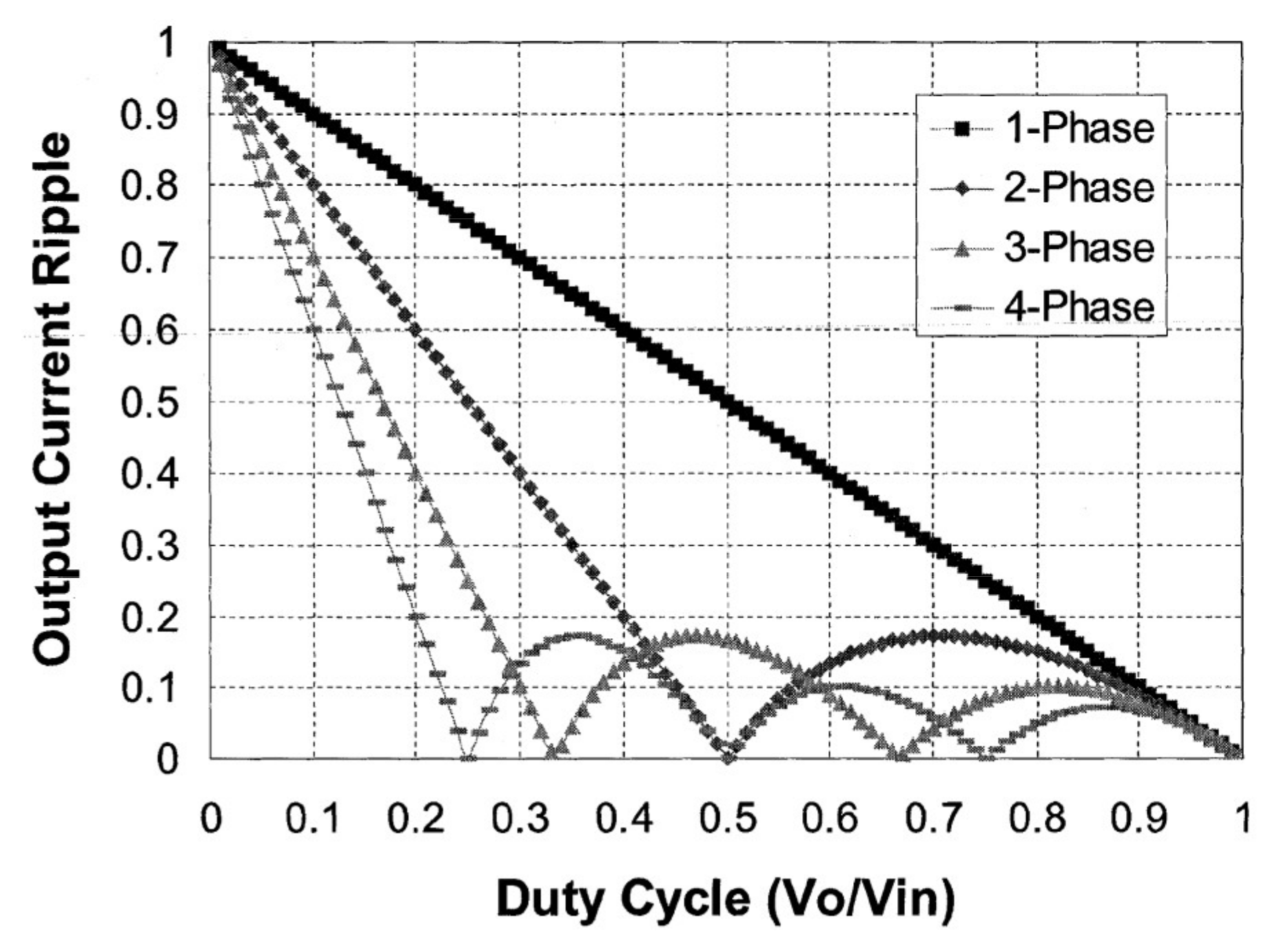
:1. Introduction
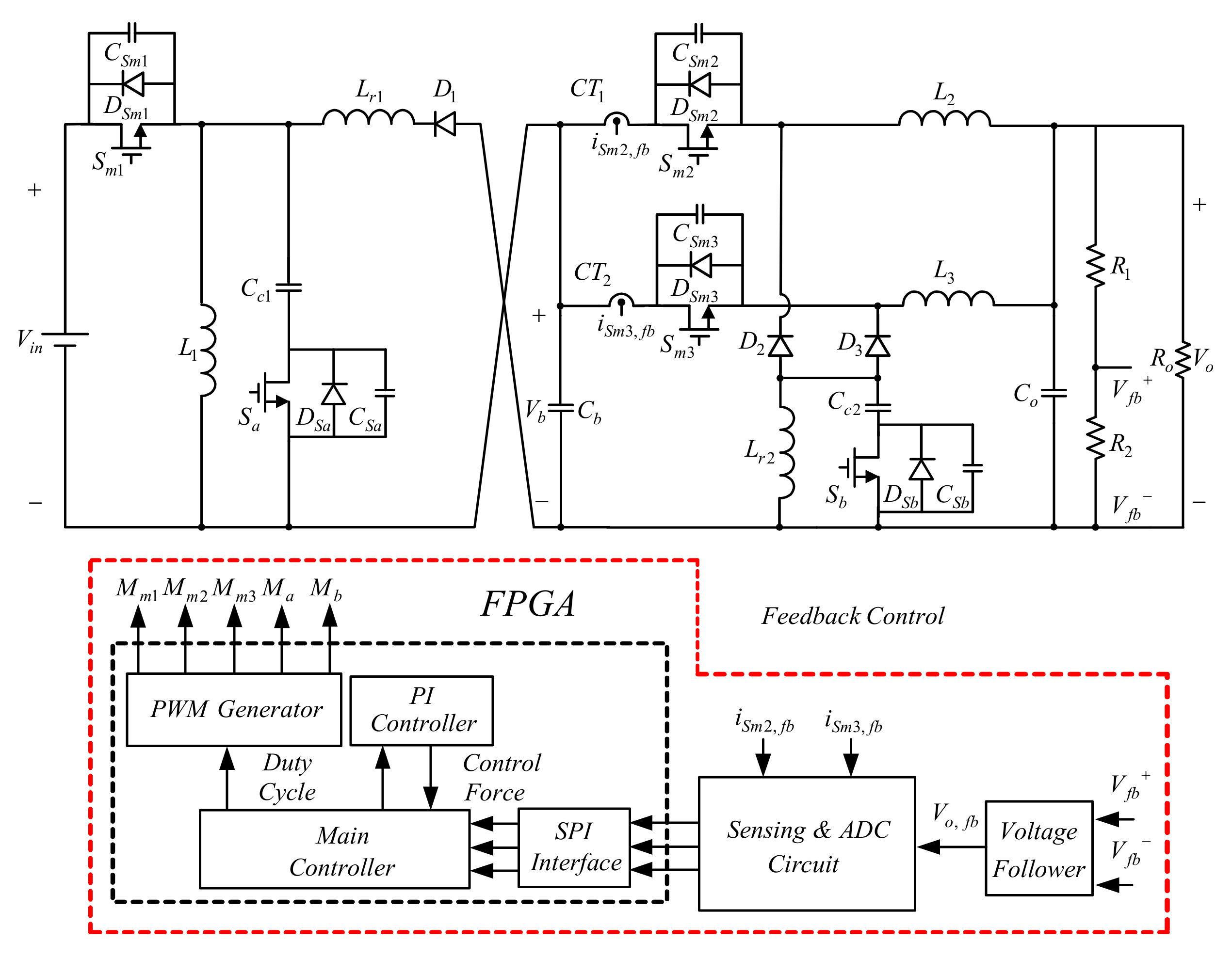
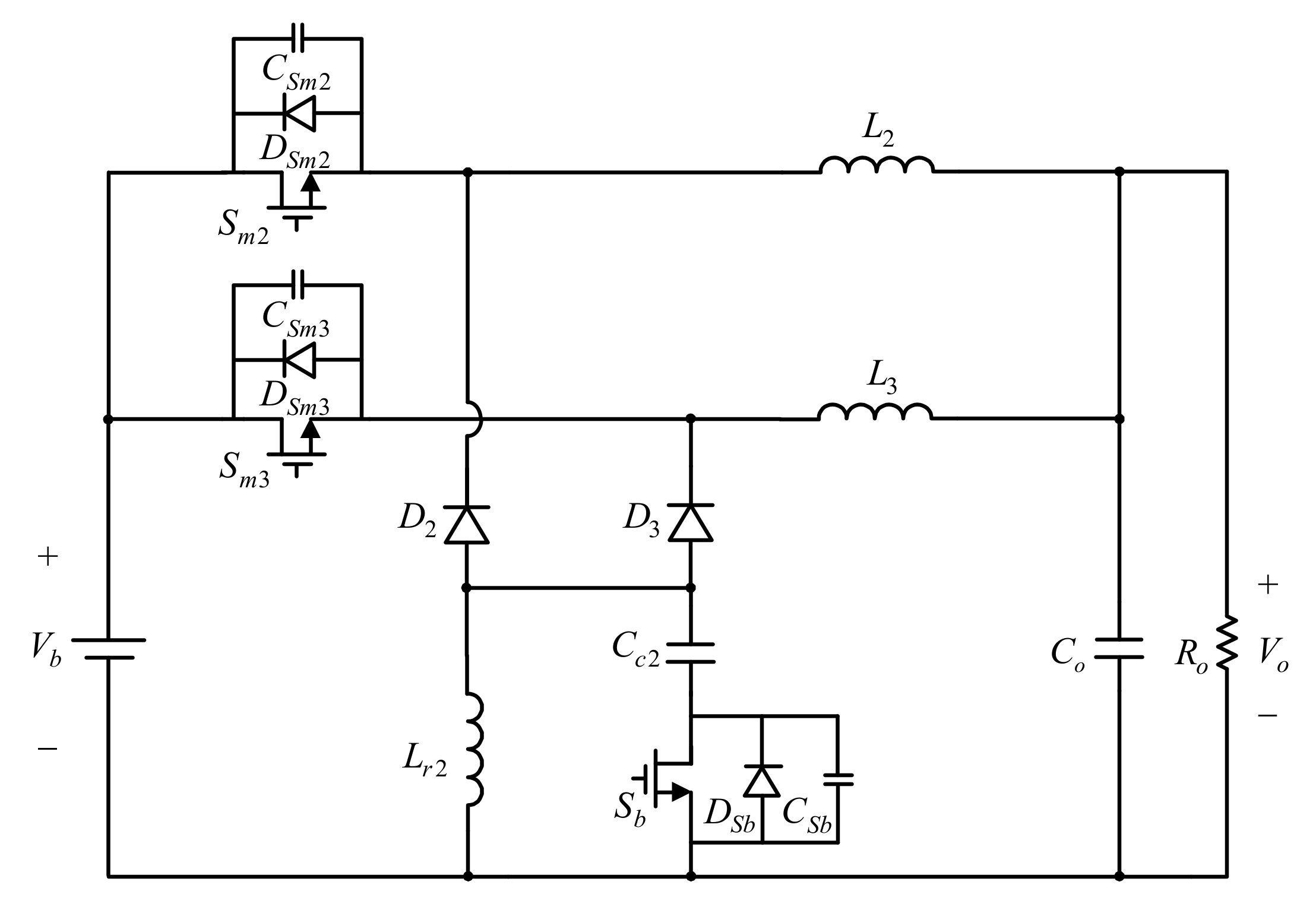
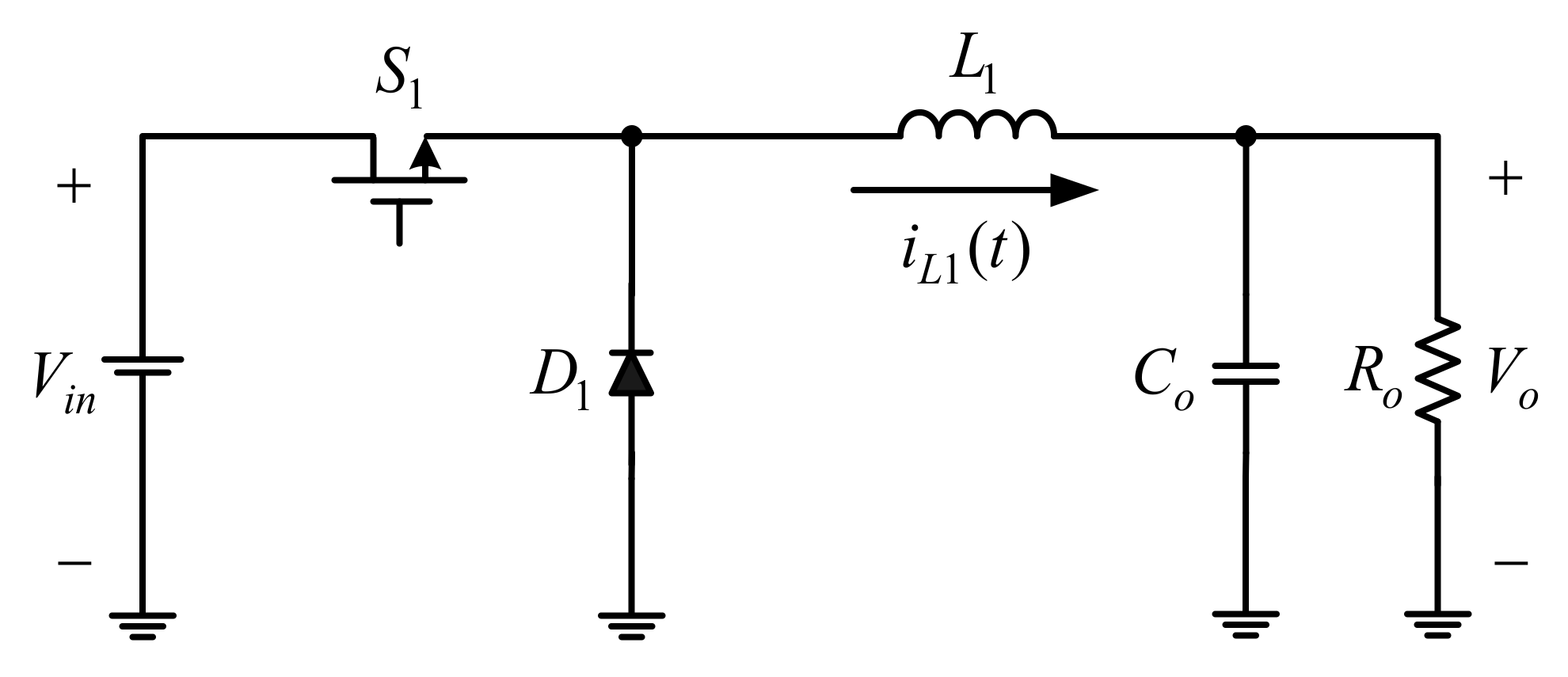
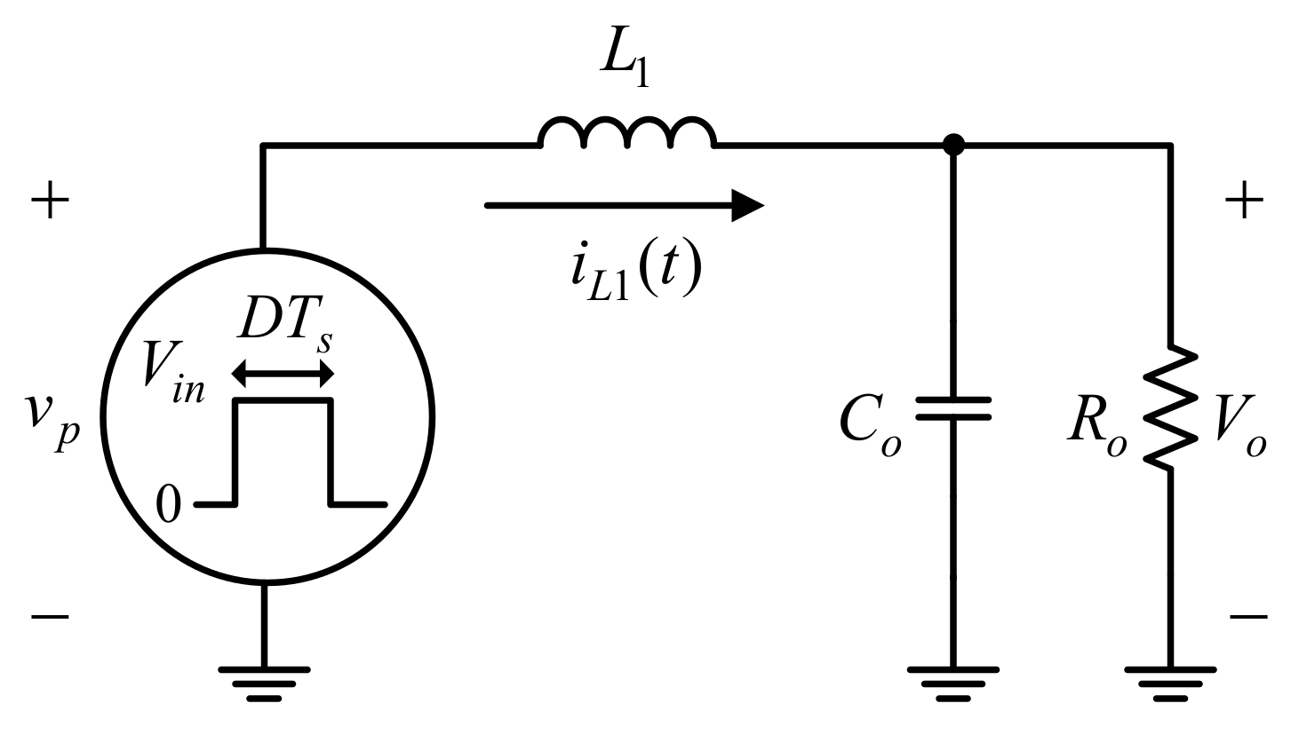
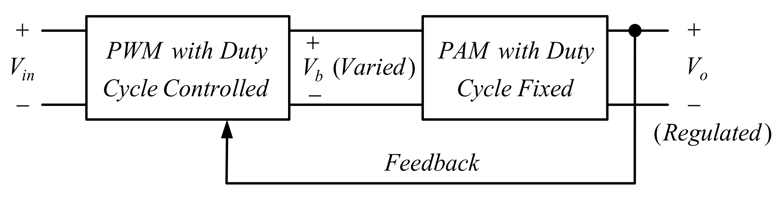
2. Proposed Circuit System
3. Basic Operating Principles
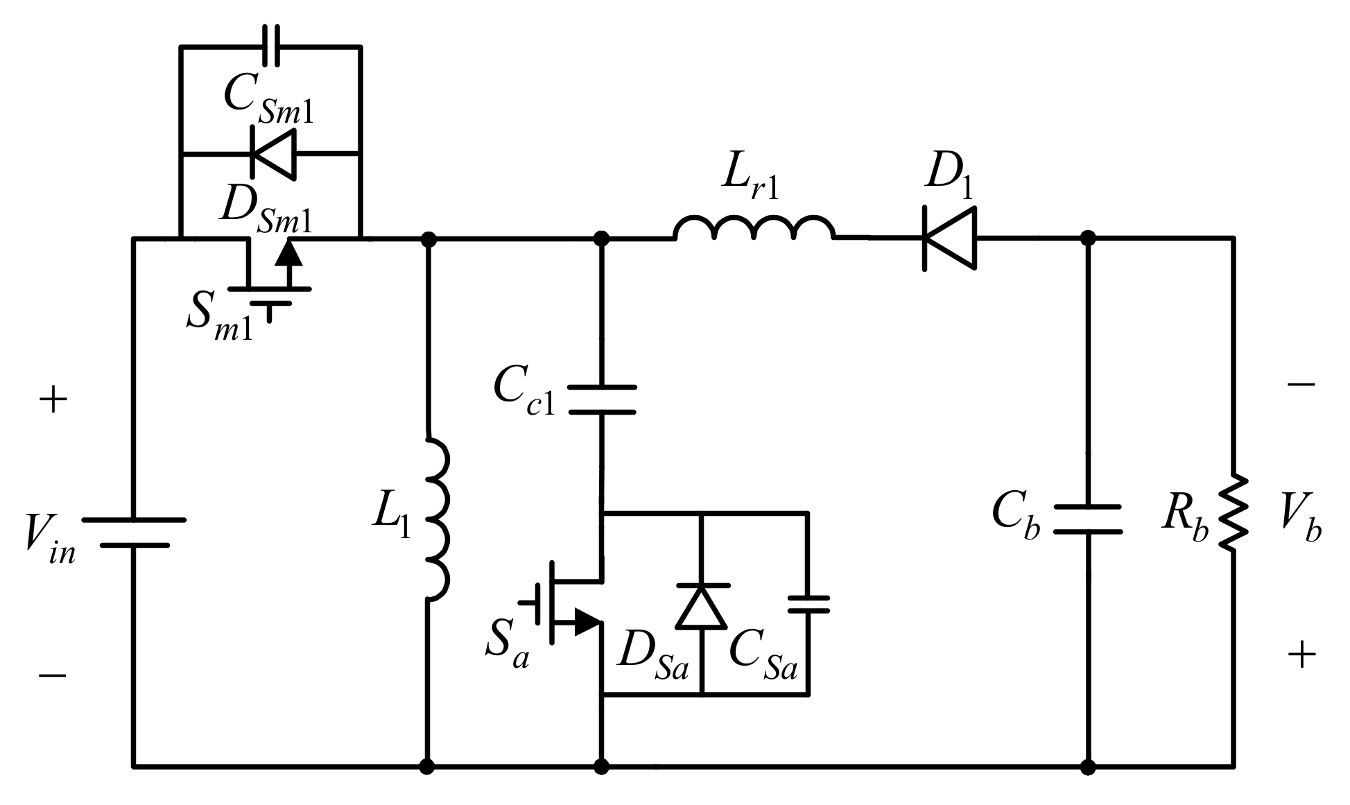
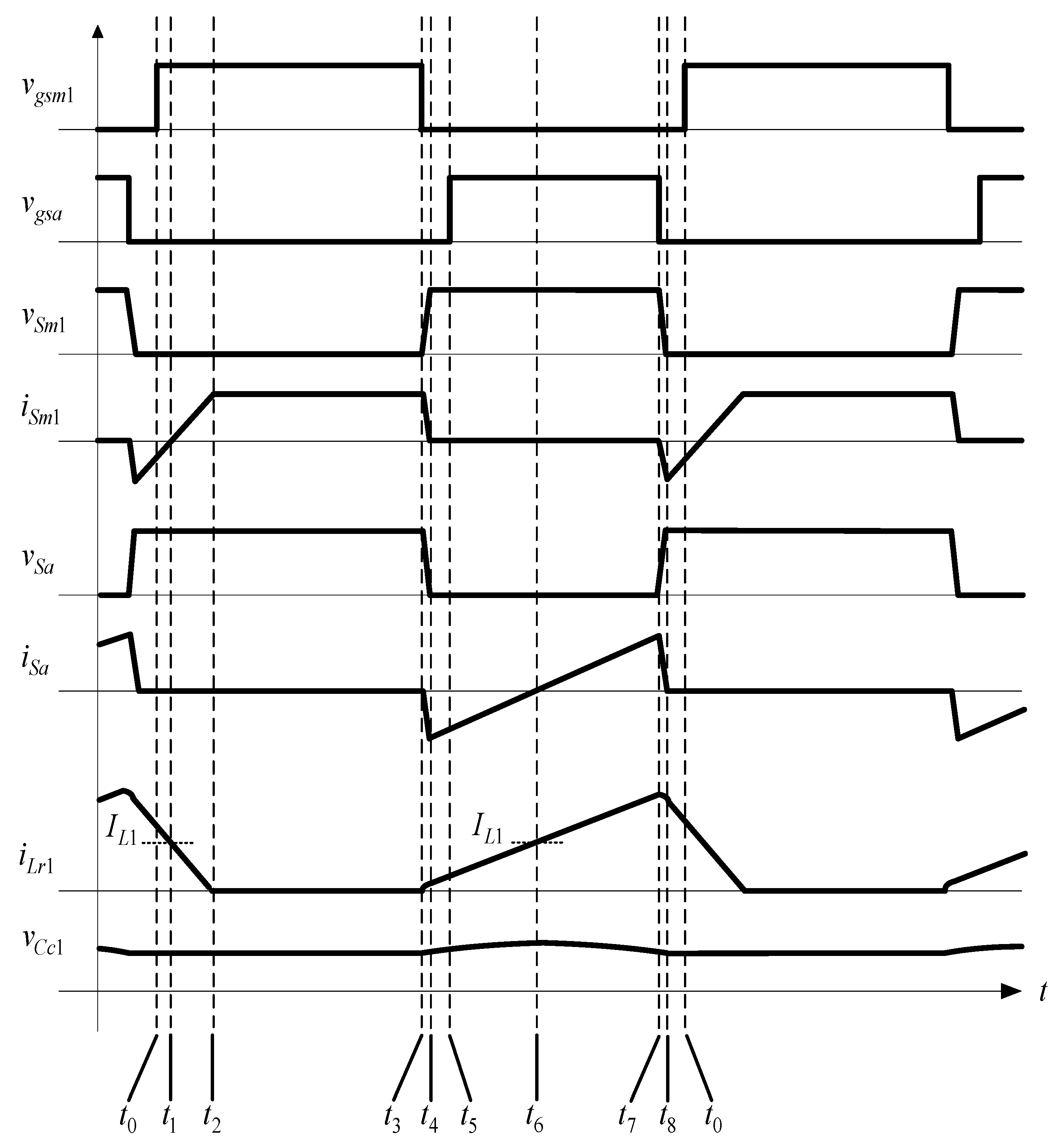
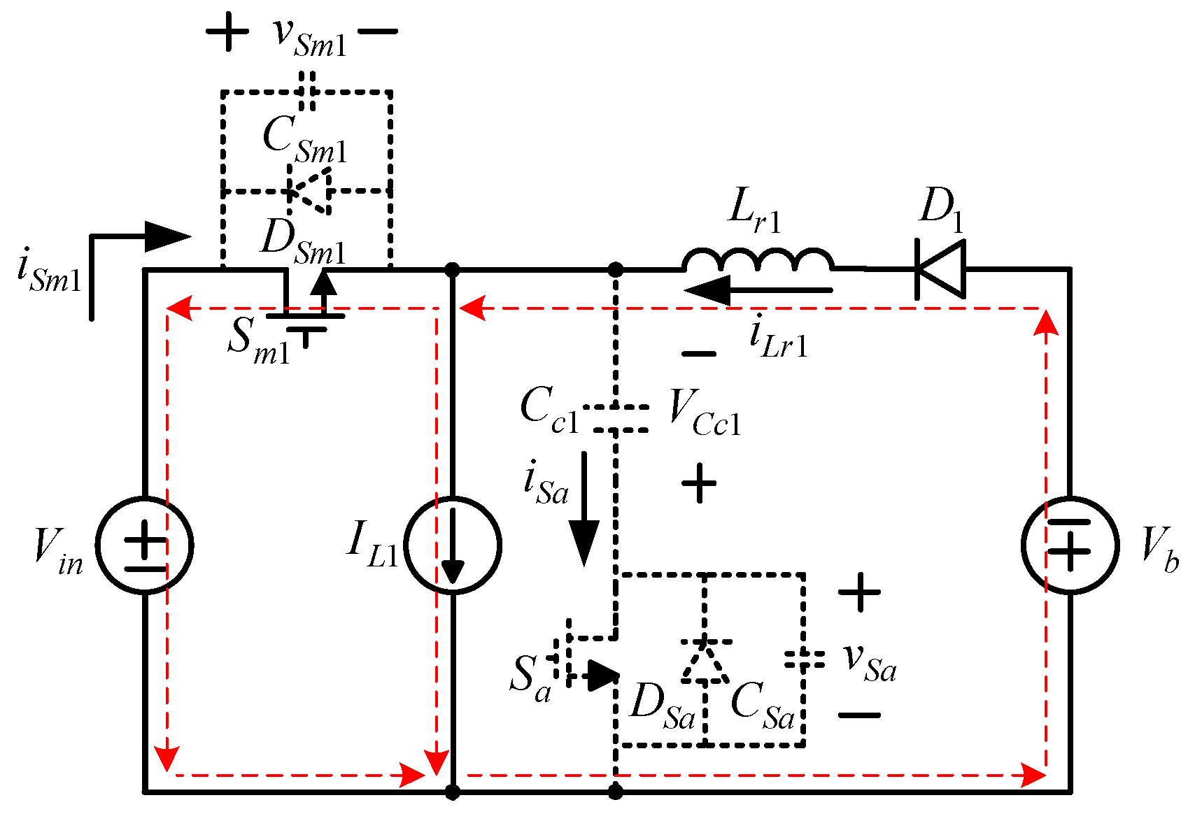
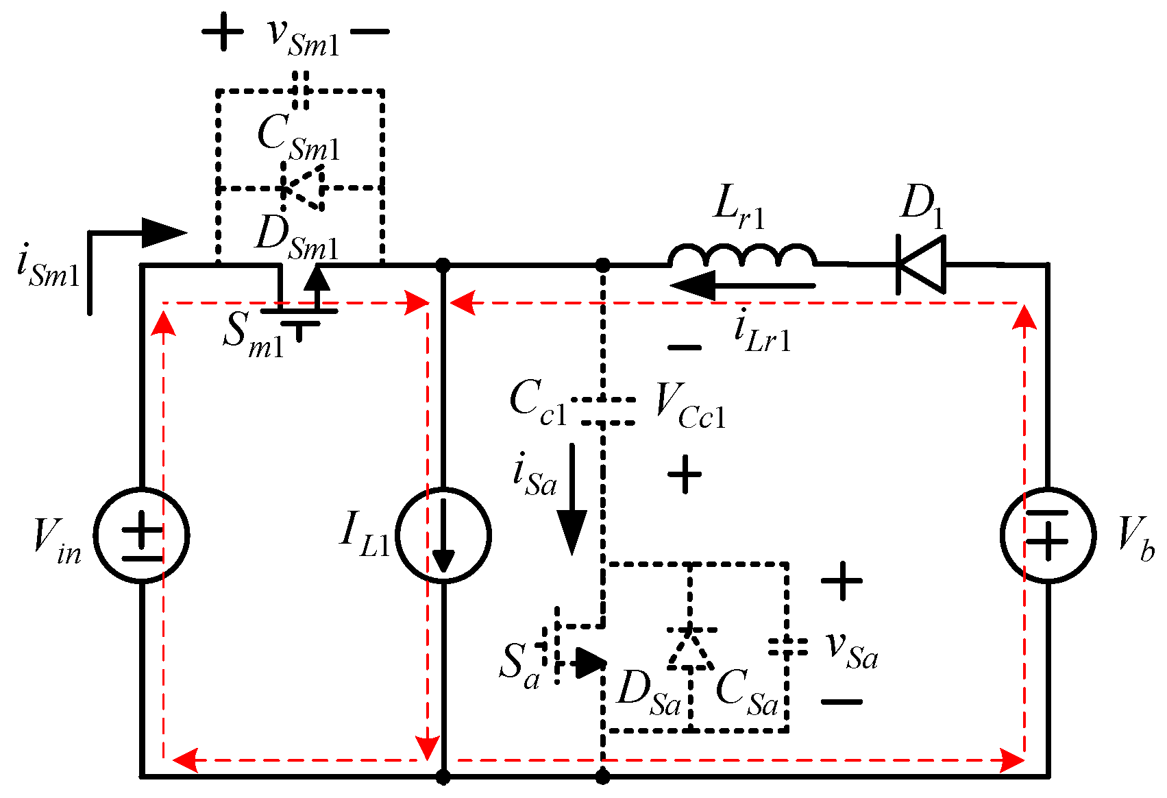
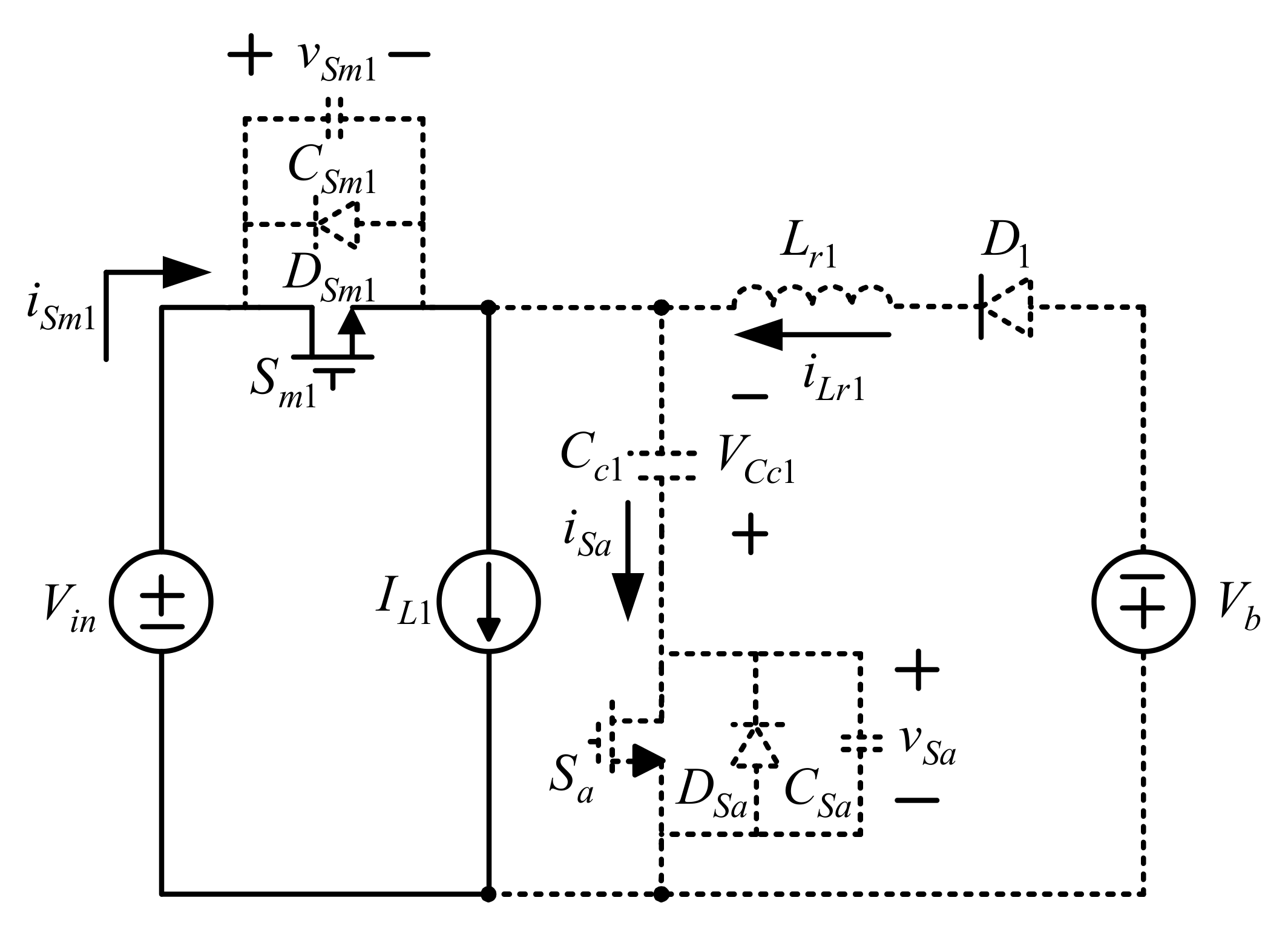
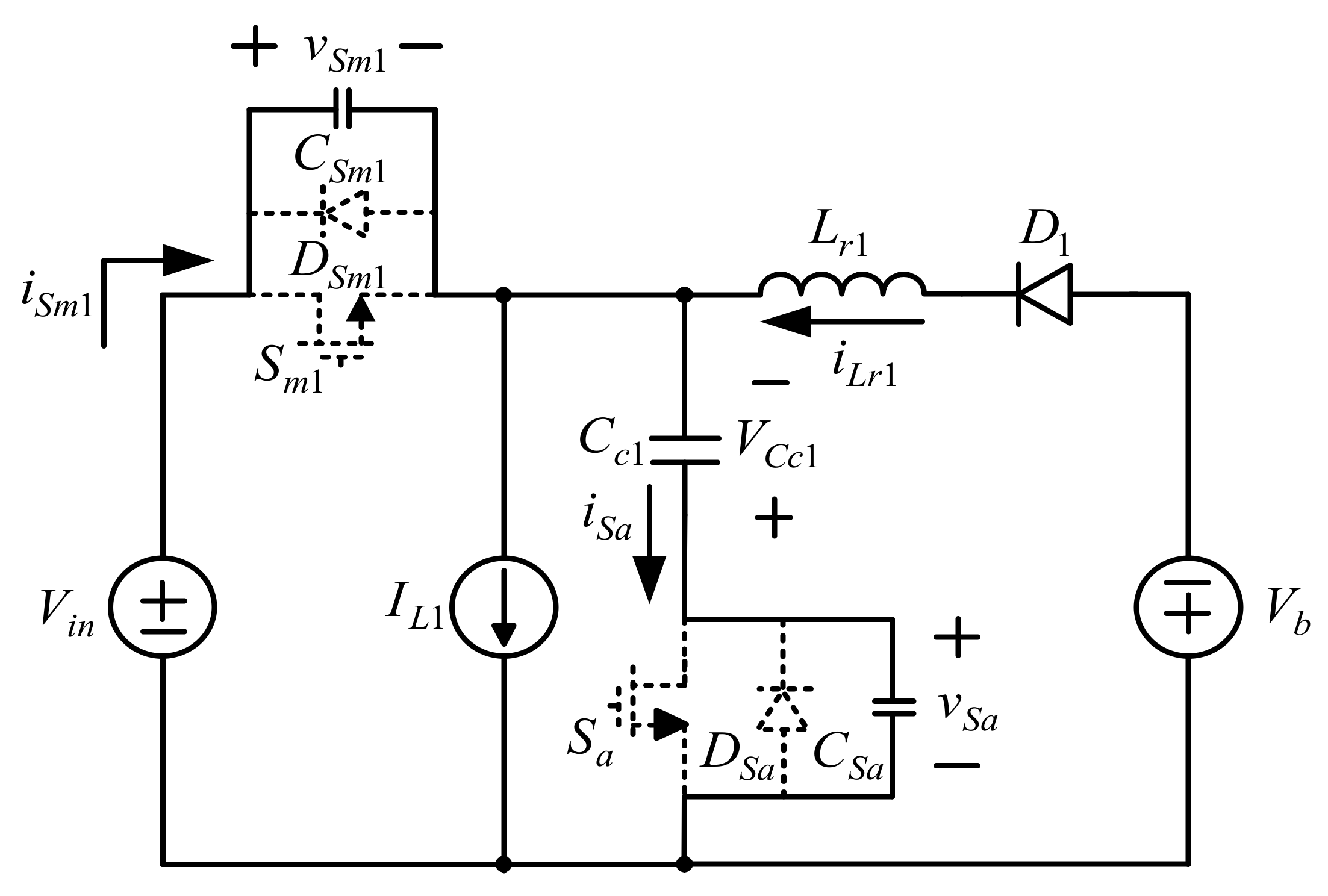
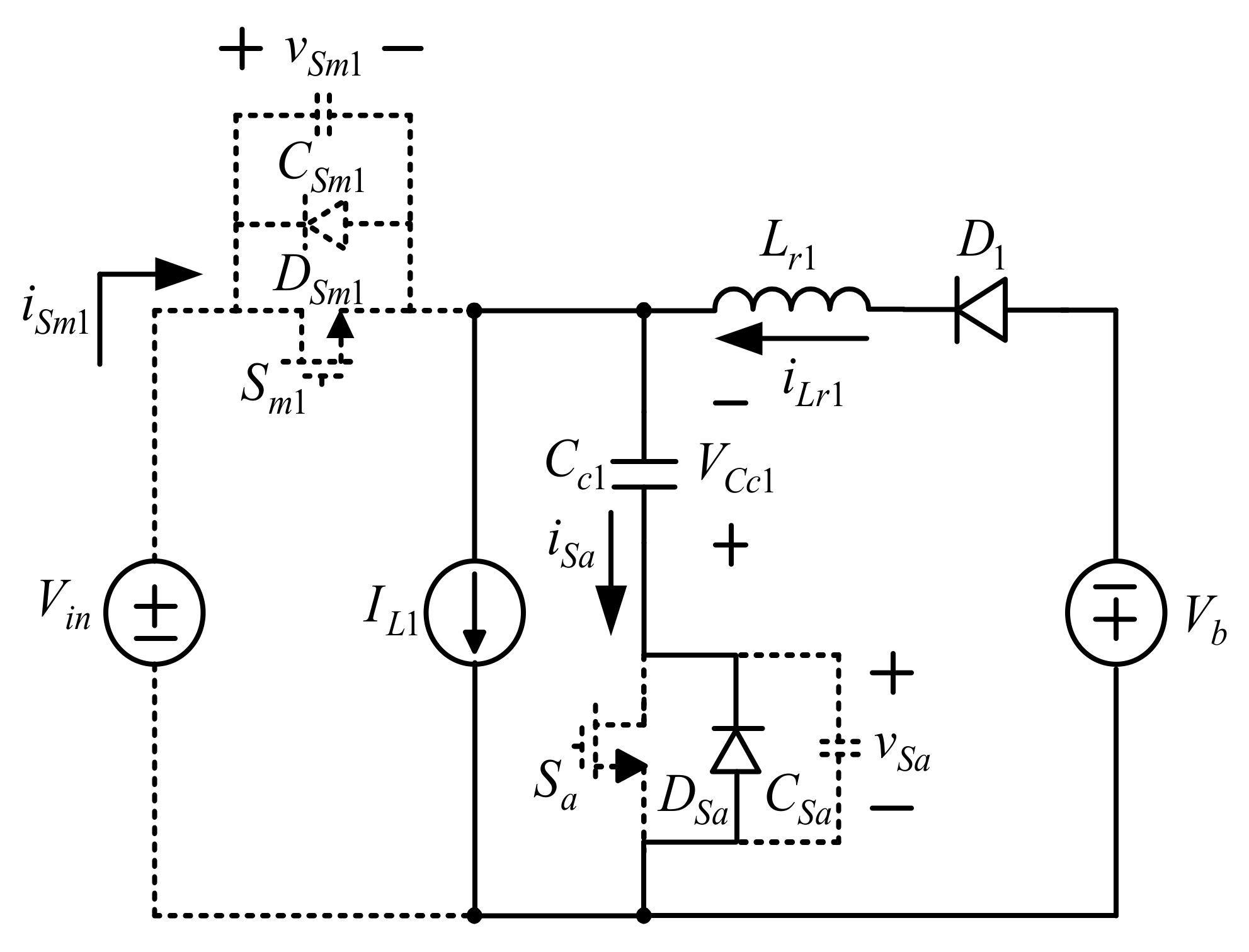
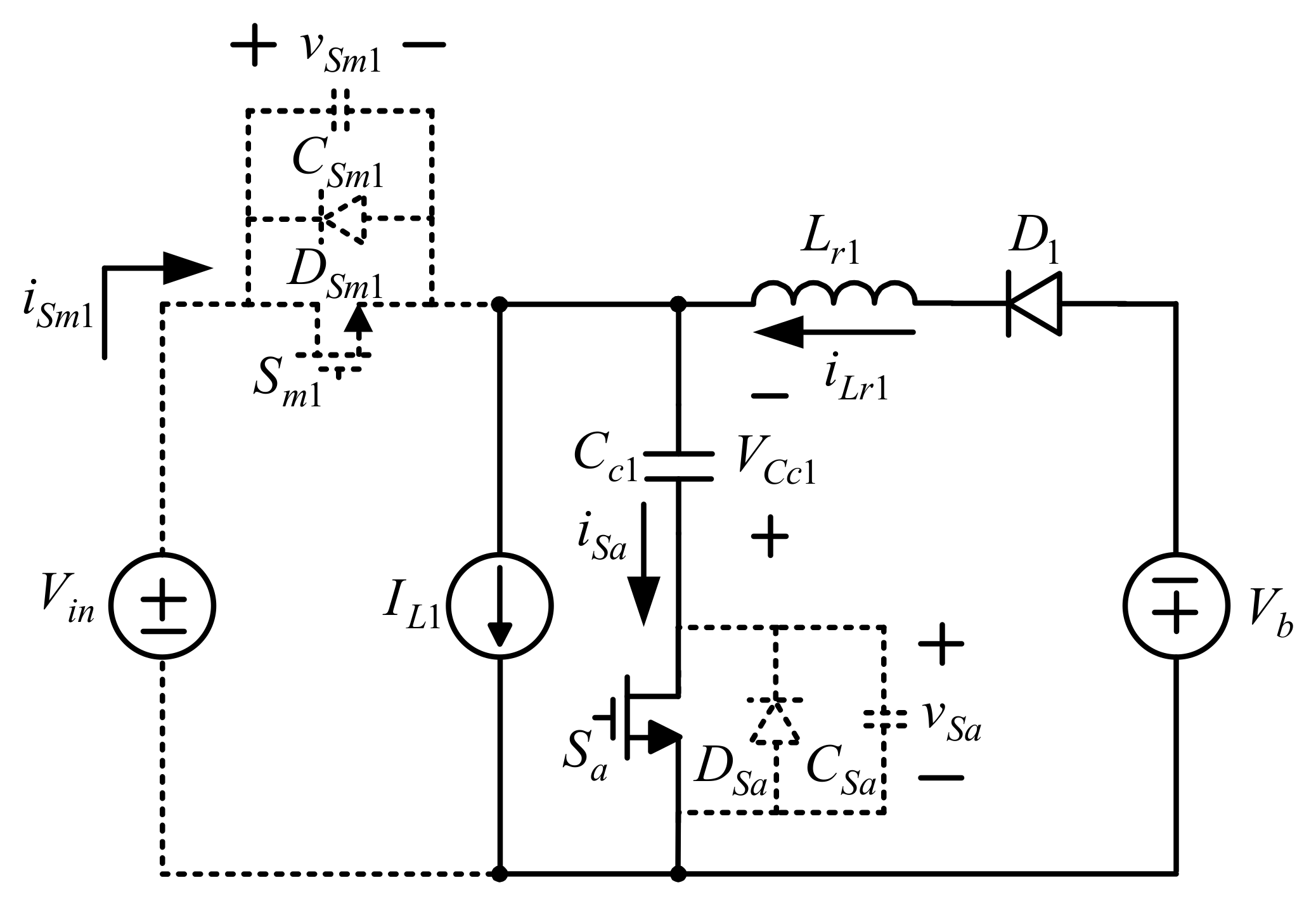
3.1. First-Stage Operating Principles
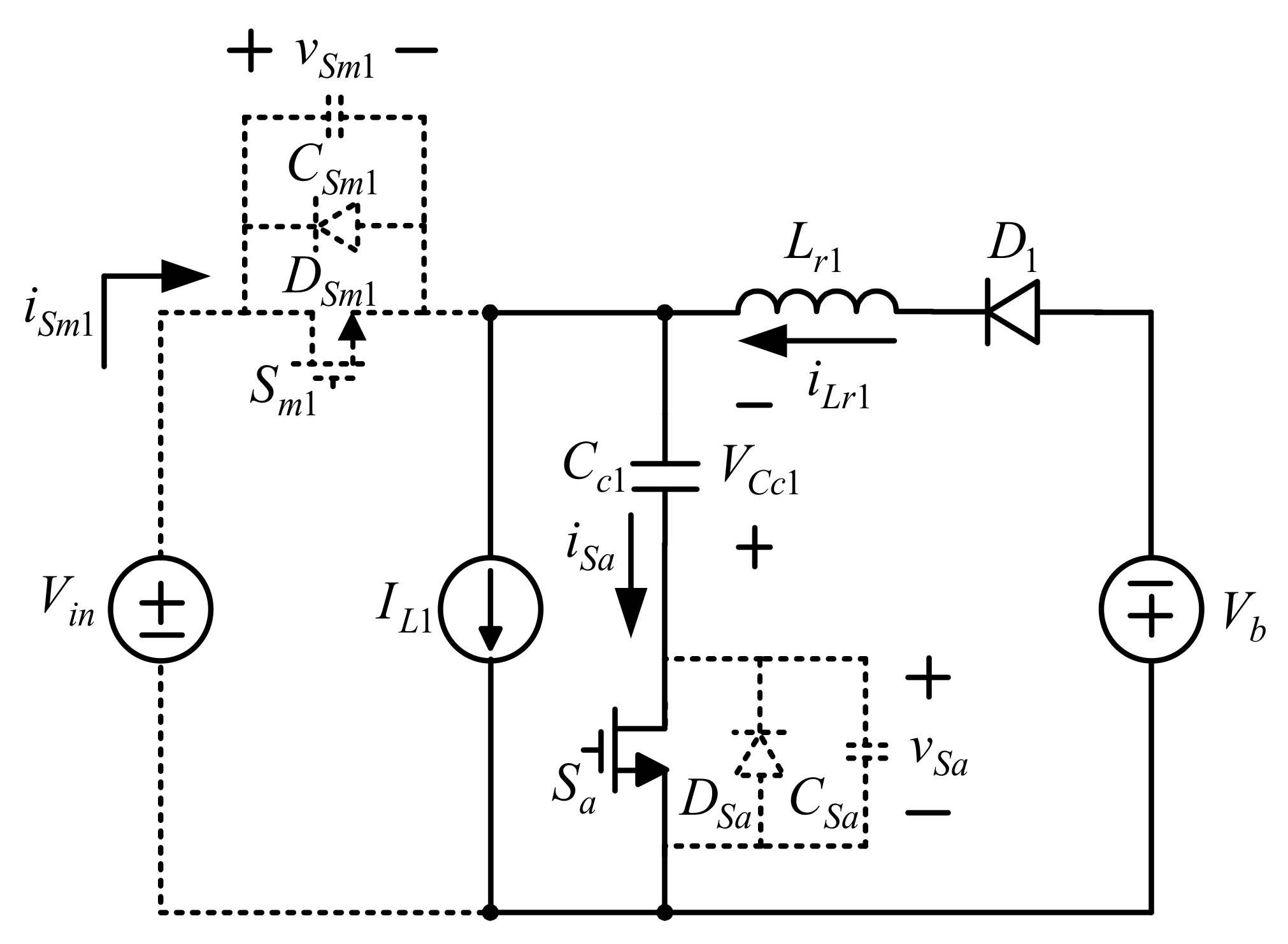
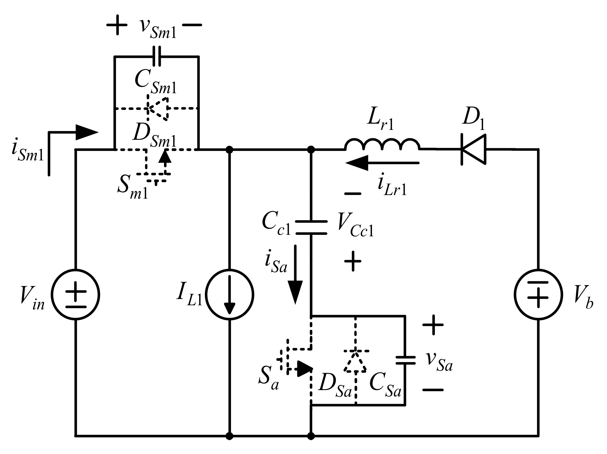
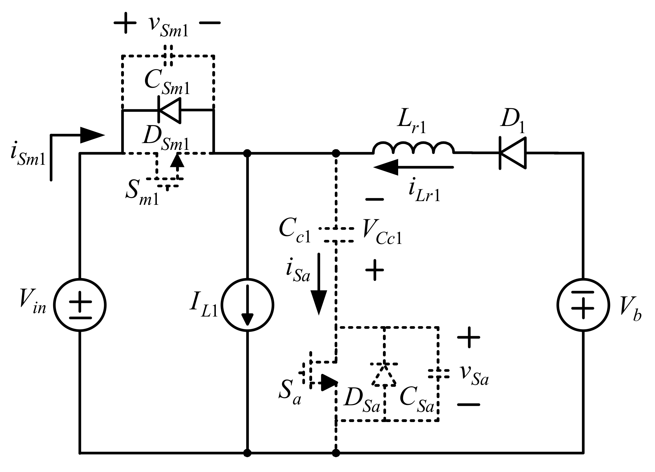
3.1.1. State 1: []
3.1.2. State 2: []
3.1.3. State 3: []
3.1.4. State 4: []
3.1.5. State 5: []
3.1.6. State 6: []
3.1.7. State 7: []
3.1.8. State 8: []
3.1.9. State 9: []
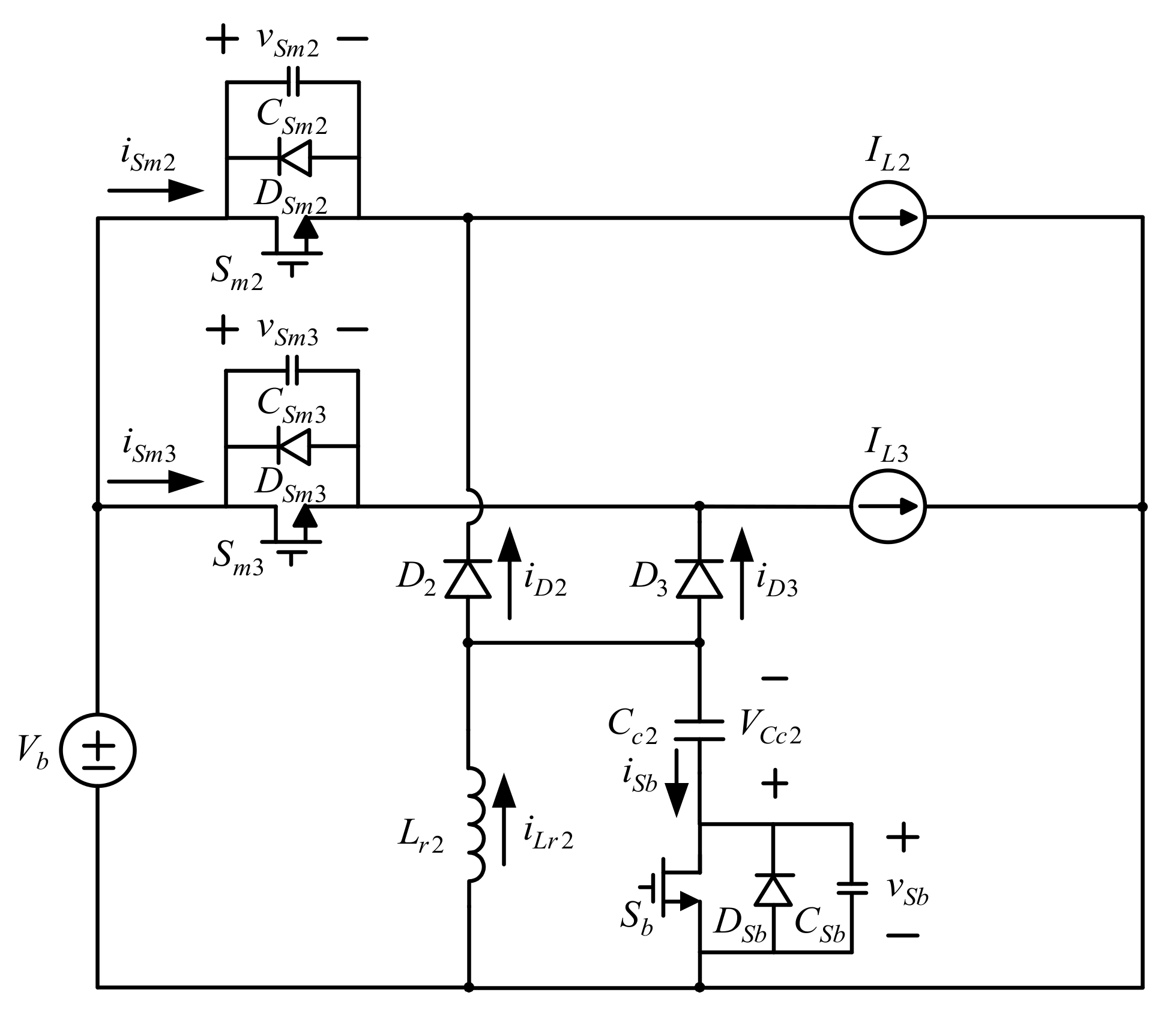
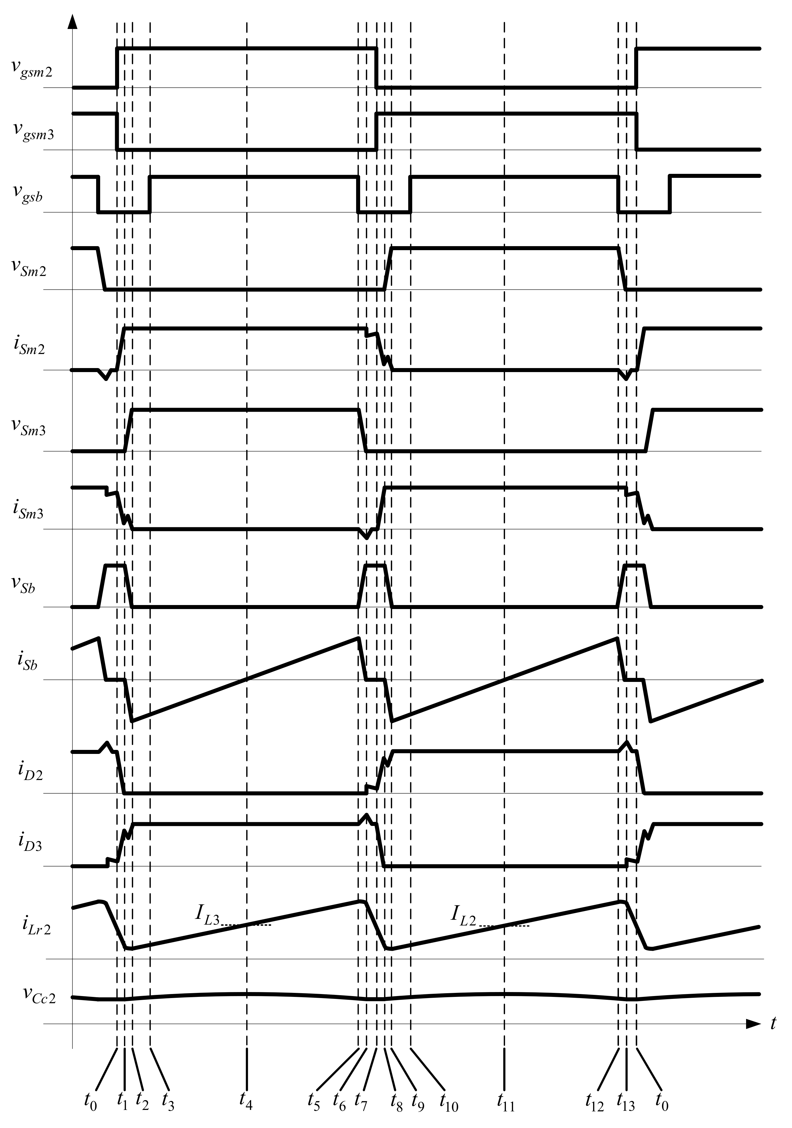
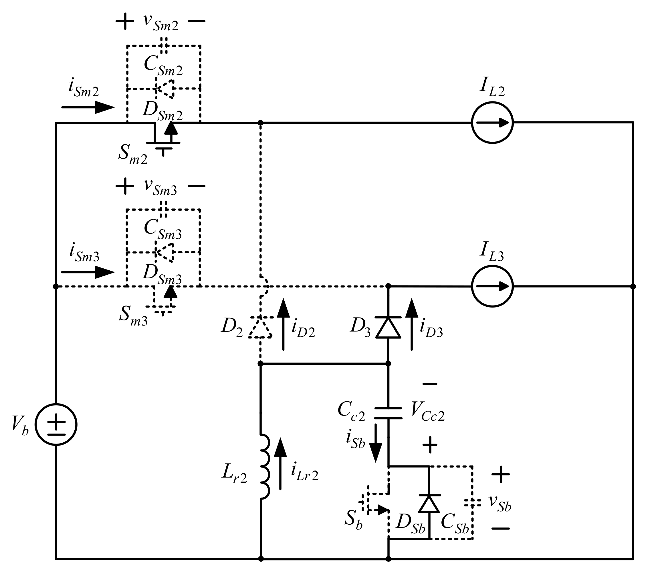
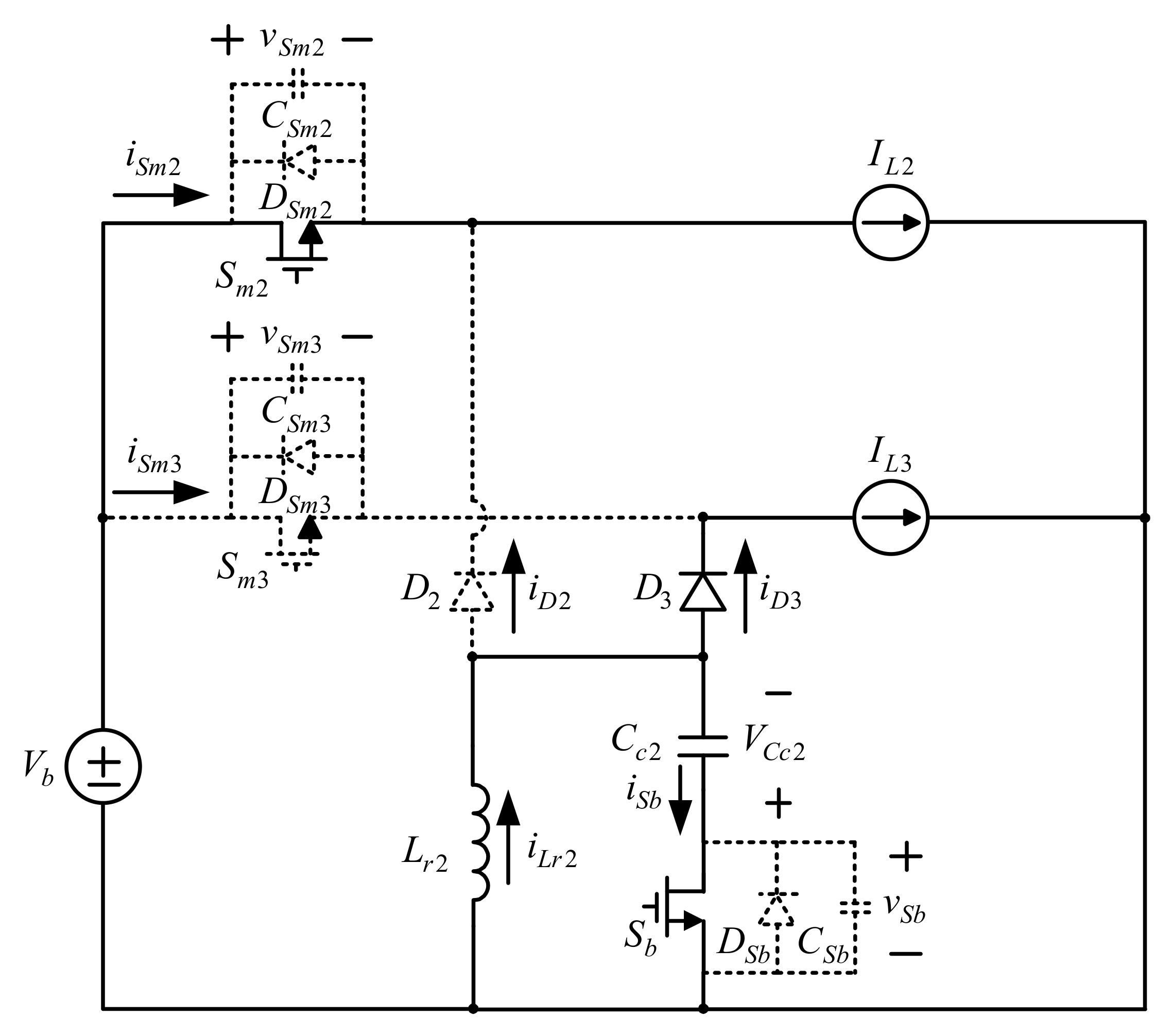
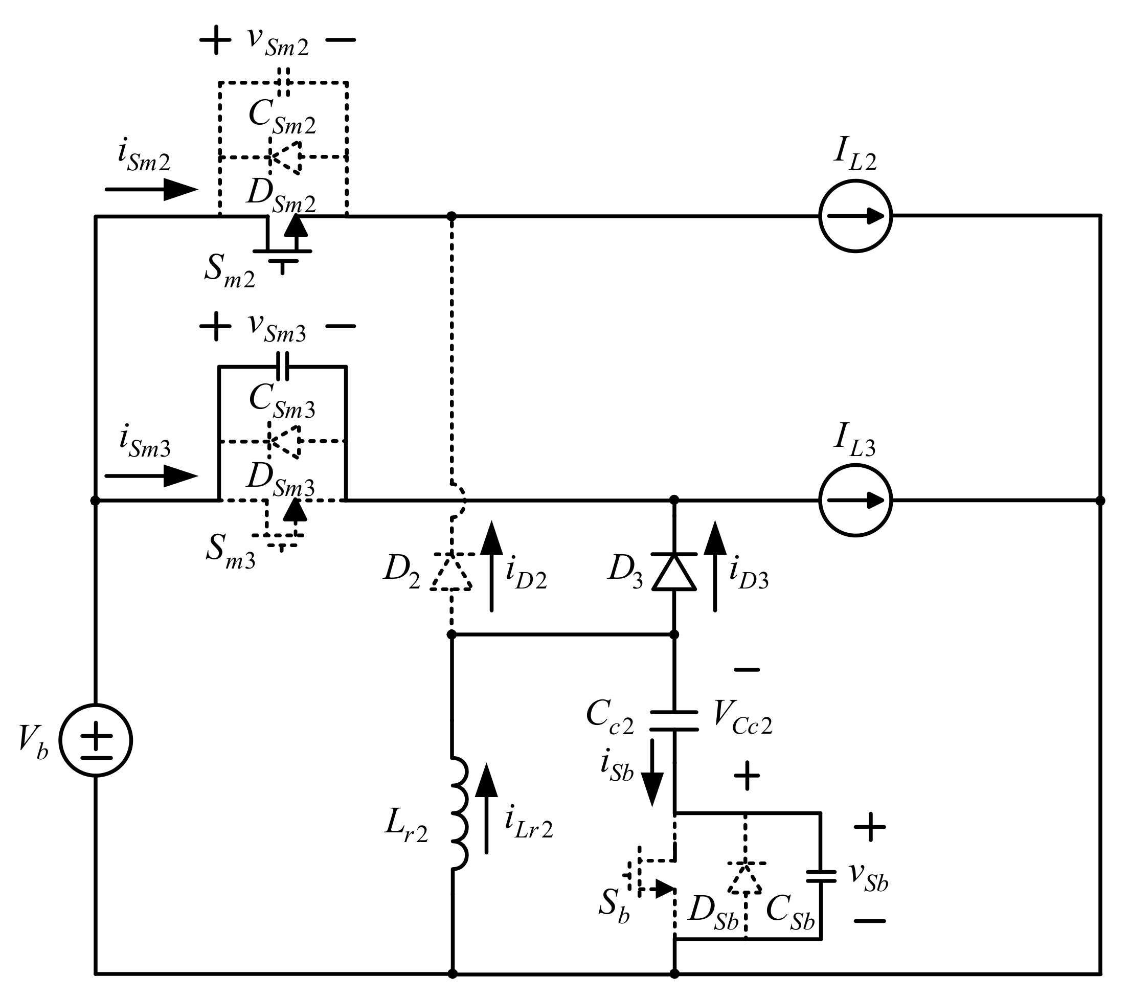
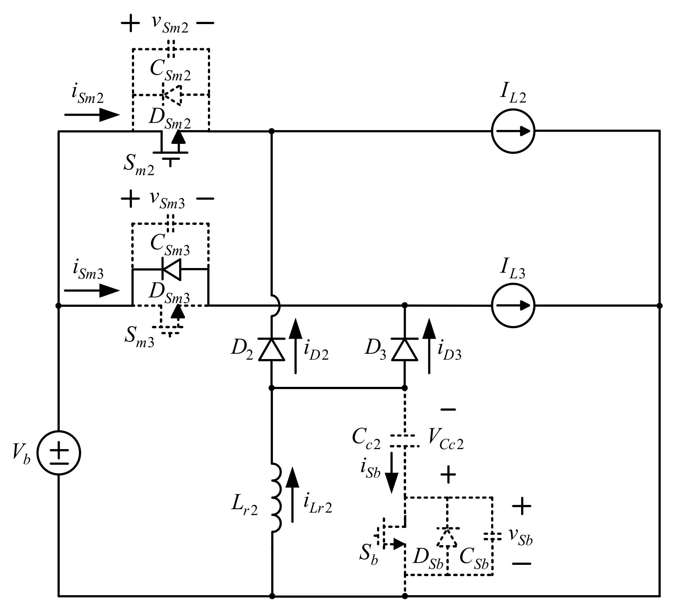
3.2. Second Stage
3.2.1. State 1: []
3.2.2. State 2: []
3.2.3. State 3: []
3.2.4. State 4: []
3.2.5. State 5: []
3.2.6. State 6: []
3.2.7. State 7: []
4. Control Strategy
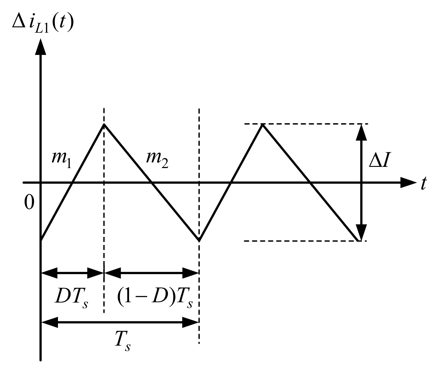
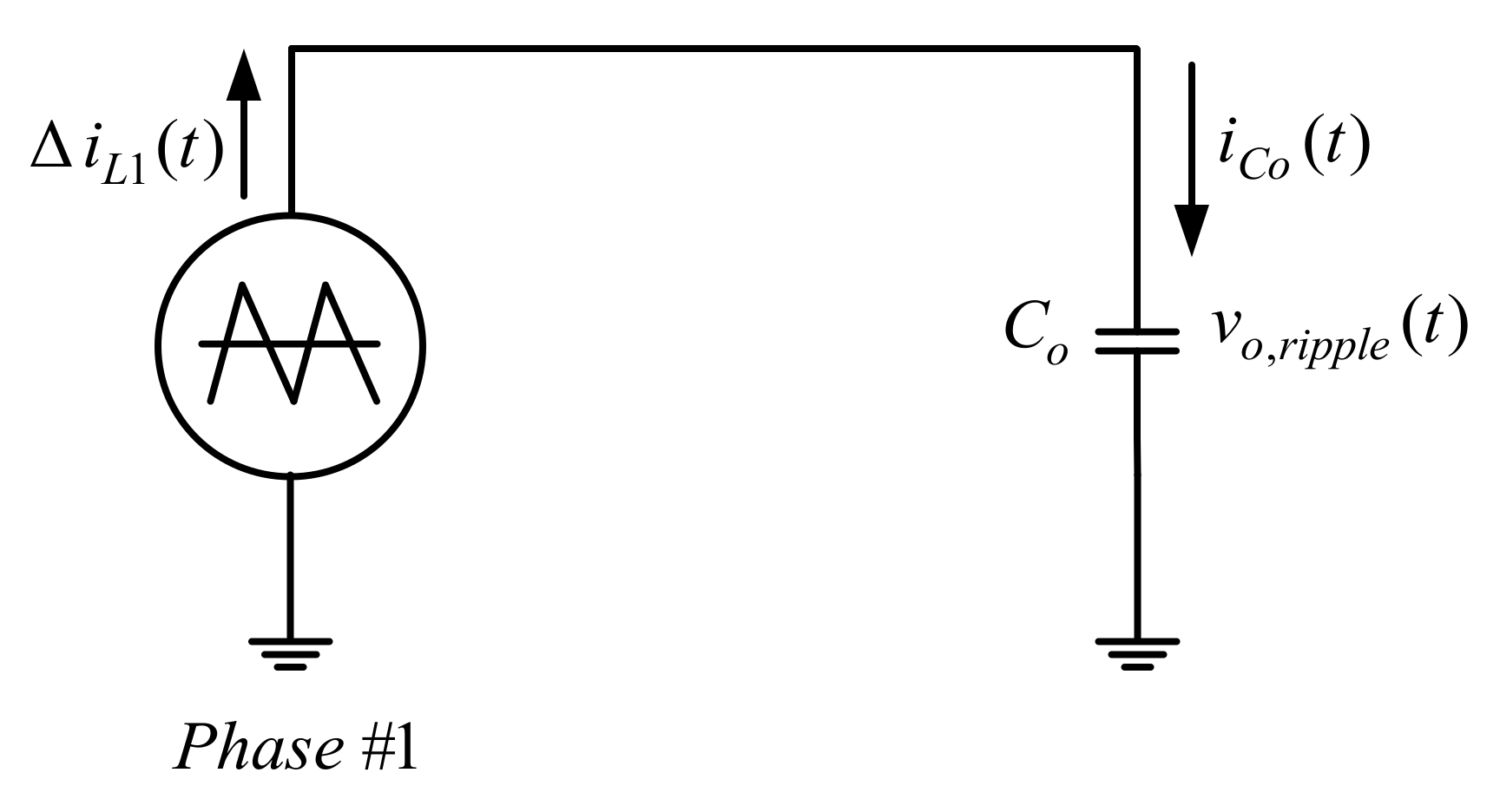
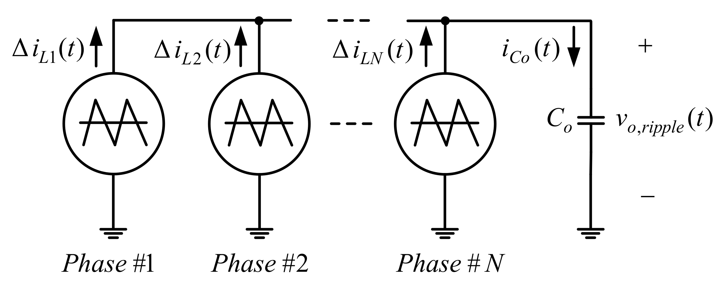
4.1. Output Voltage Ripple Minimization
4.2. Output Voltage Regulation
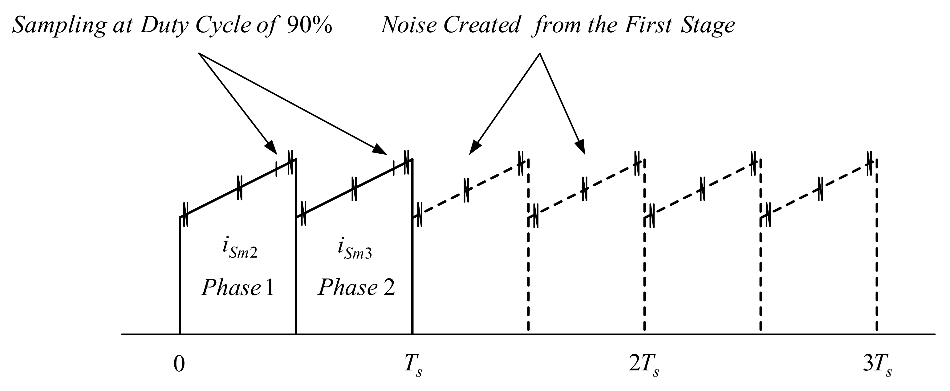
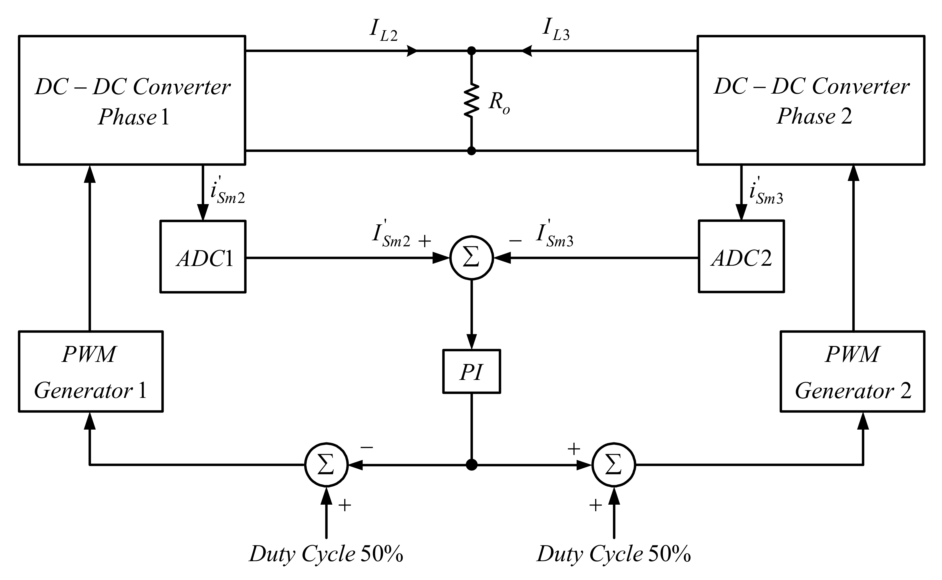
4.3. Current-Sharing Control
5. Design of Resonant Inductor and Clamp Capacitor
5.1. Design of First-Stage Resonant Inductor Lr1
5.2. Design of First-Stage Voltage Clamp Capacitor Cc1
5.3. Design of Second-Stage Resonant Inductor Lr2
5.4. Design of Second-Stage Voltage Clamp Capacitor Cc2
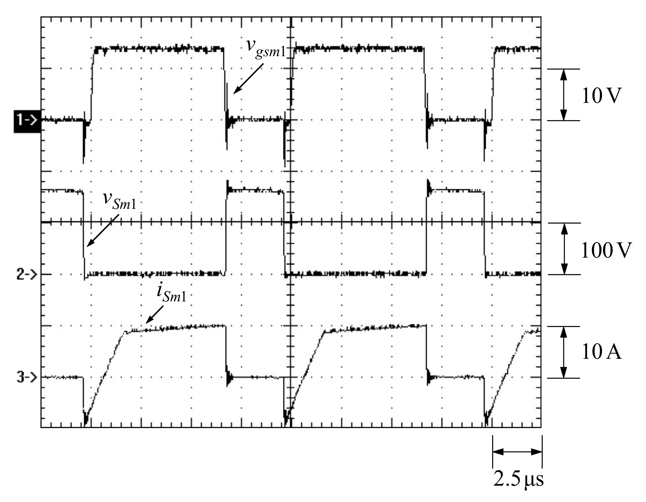
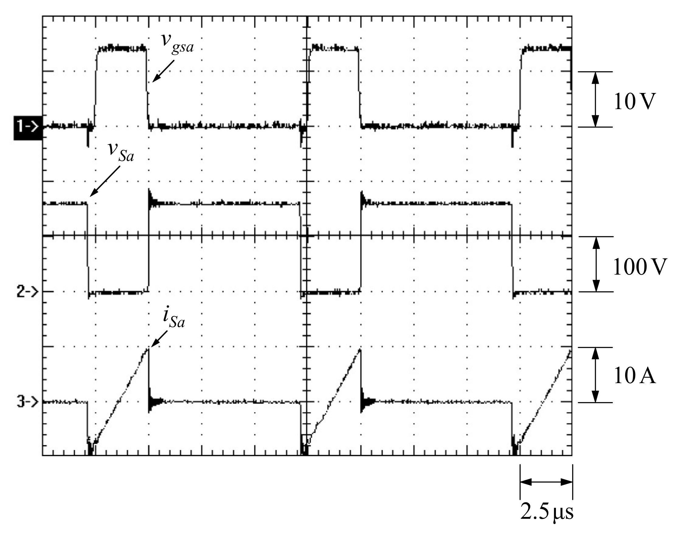
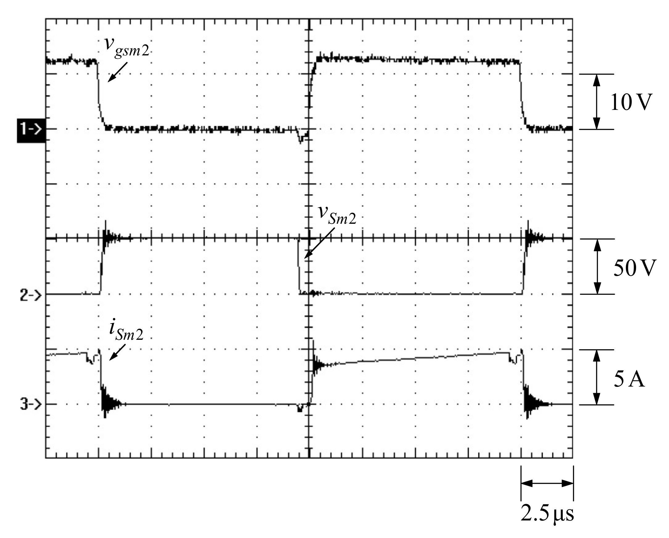
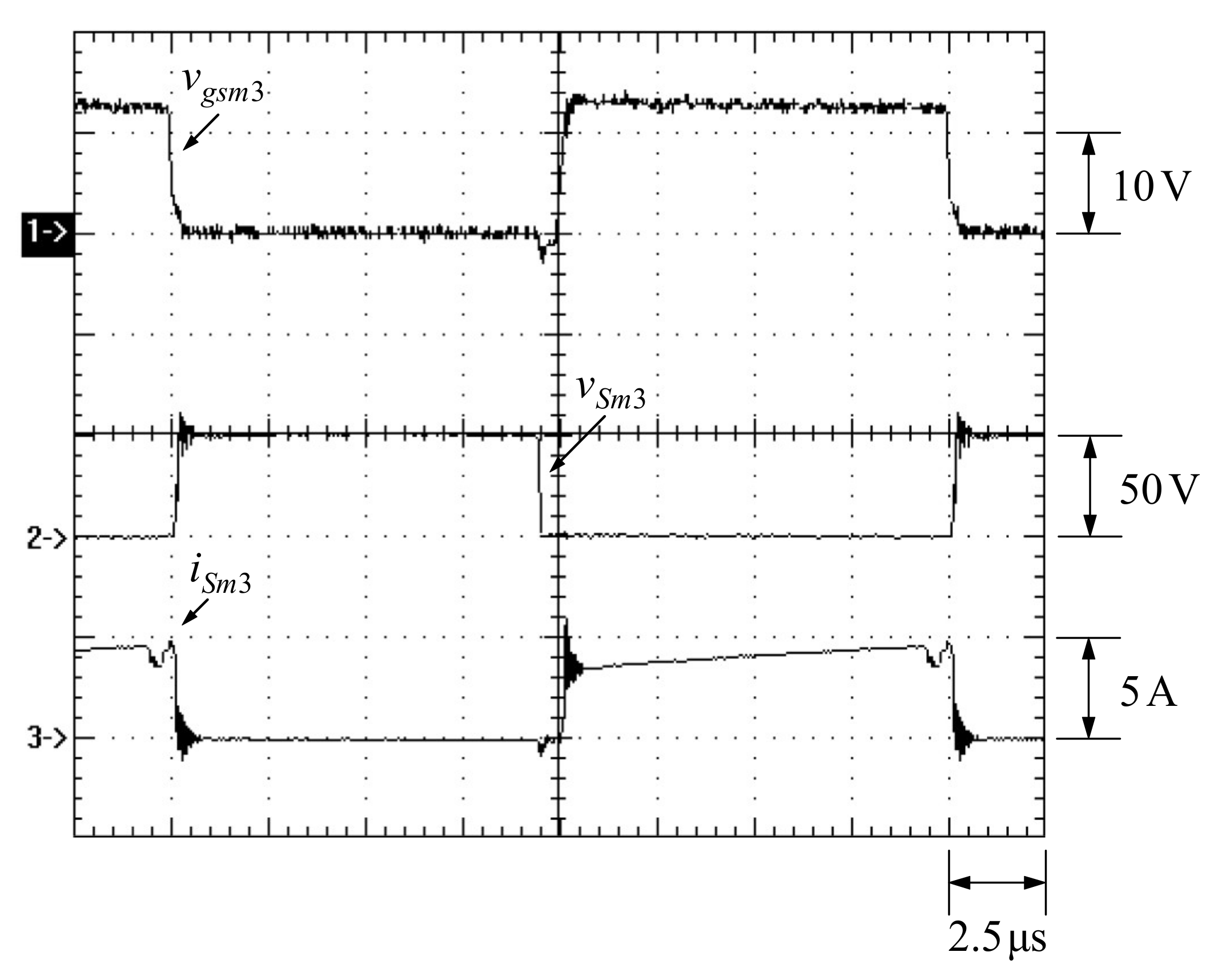
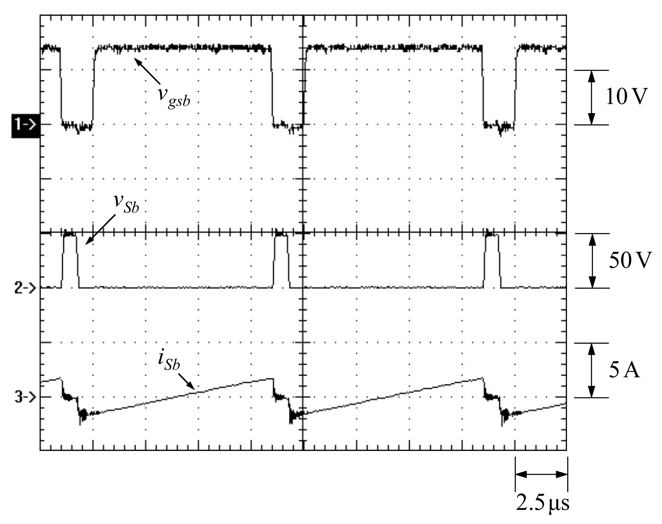
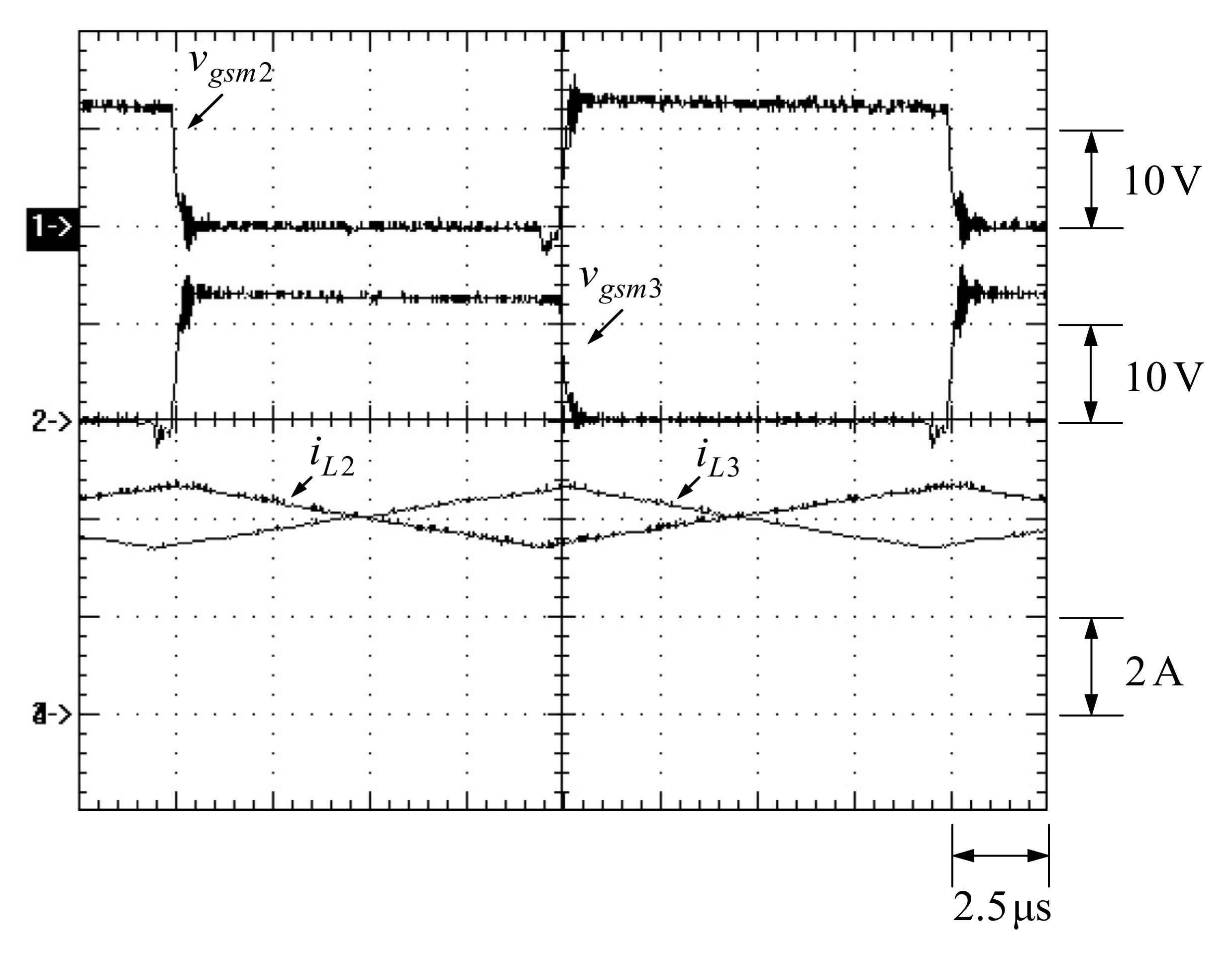
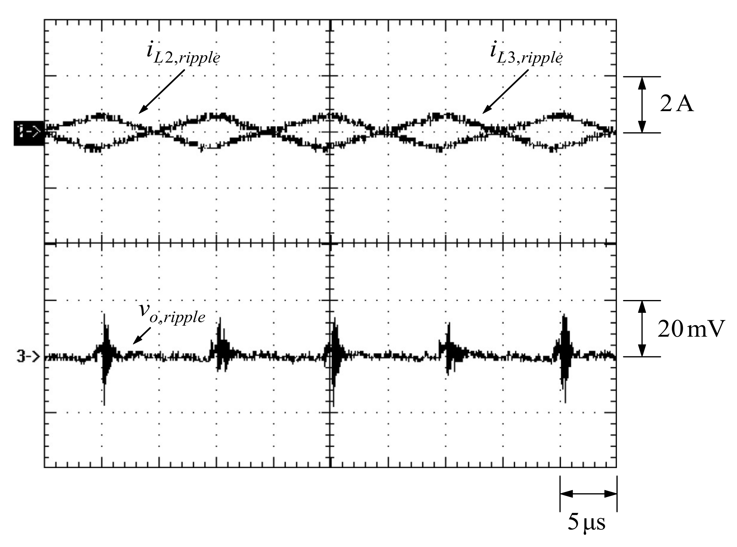
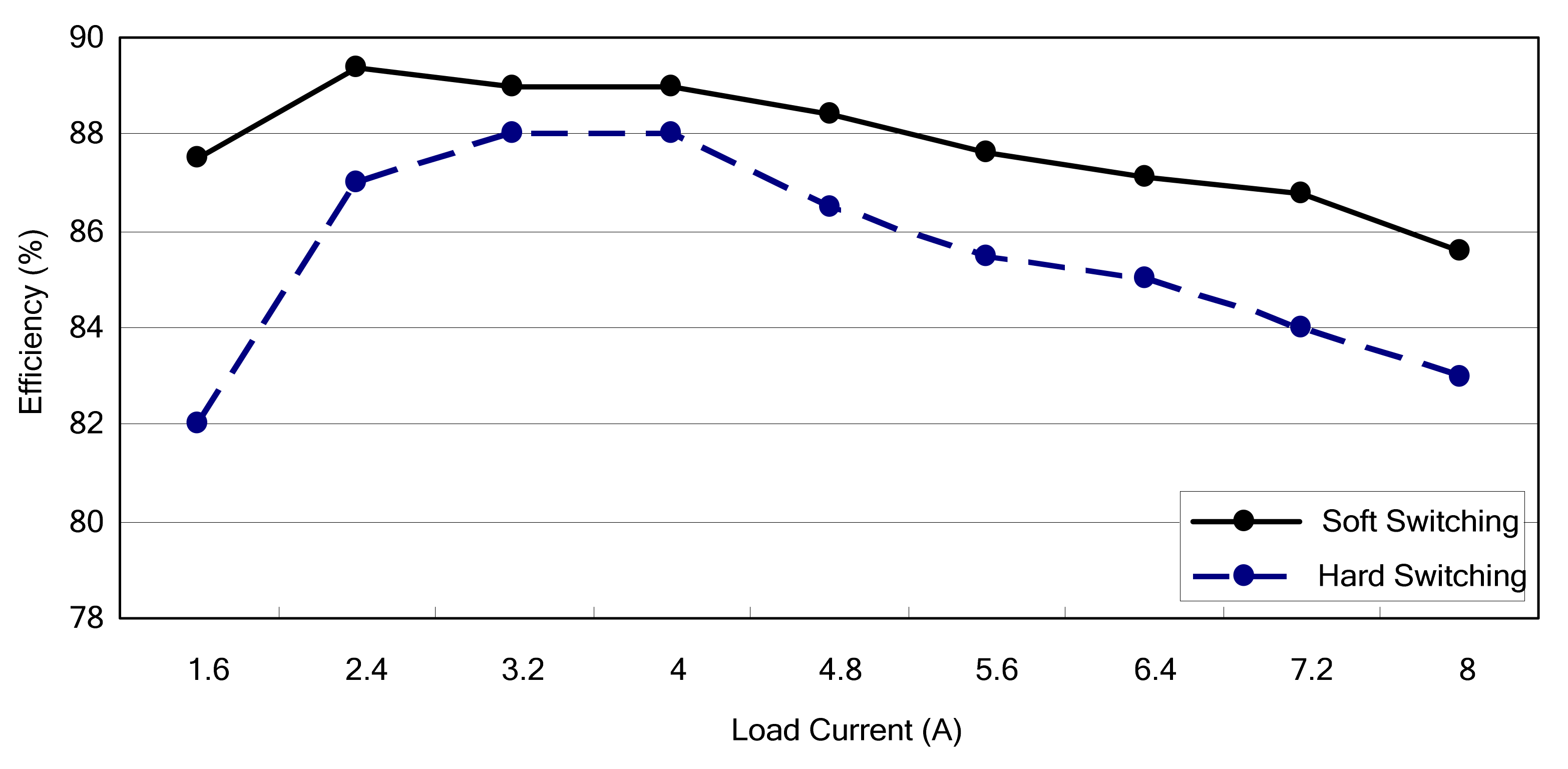
6. Experimental Results
7. Output Voltage Ripple Comparison
8. Conclusions
- (1)
- This two-stage converter has only a single feedback control loop under PWM control, which is applied to the first stage.
- (2)
- The second stage is under PAM control with the fixed duty cycle of about 0.5.
- (3)
- Due to PAM control with the fixed duty cycle of about 0.5 plus current-sharing control, the output voltage ripple of the second stage is quite small, about 8 mV, independent of the input voltage.
- (4)
- Two phases of the second stage use only one resonant tank. Three phases or more with only one resonant tank will work also.
- (5)
- Two stages have the proposed active clamp circuits to make the main and auxiliary switches all have ZVS turn-on, thus improving the overall conversion efficiency.
Author Contributions
Funding
Institutional Review Board Statement
Informed Consent Statement
Data Availability Statement
Acknowledgments
Conflicts of Interest
References
- Yang, X.; Zong, S.; Fan, G. Analysis and Validation of the Output Current Ripple in Interleaved Buck Converter. In Proceedings of the IECON 2017—43rd Annual Conference of the IEEE Industrial Electronics Society, Beijing, China, 29 October–1 November 2017; pp. 846–851. [Google Scholar] [CrossRef]
- Wang, L.; Zhang, D.; Zha, D.; Duan, J.; Li, J. Six-phase Symmetric Inverse Fully Coupled Non-Isolated Interleaved Bidirectional Buck/Boost Converter with Low Current Ripples High Dynamic Response. In Proceedings of the 2018 IEEE International Power Electronics and Application Conference and Exposition (PEAC), Shenzhen, China, 4–7 November 2018; pp. 1–6. [Google Scholar] [CrossRef]
- Sobhan, S. Comparative Assessment of Non-Isolated DC-DC Converters Combined with Passive Ripple Cancelling Circuit. In Proceedings of the 2018 10th International Conference on Electrical and Computer Engineering (ICECE), Dhaka, Bangladesh, 20–22 December 2018; pp. 357–360. [Google Scholar] [CrossRef]
- Seok, H.; Kim, S.; Choi, W.; Kim, M.; Lee, J.S.; Kim, M. Design of Zero-Voltage-Ripple Buck DC-DC Converter. In Proceedings of the 2017 IEEE 60th International Midwest Symposium on Circuits and Systems (MWSCAS), Boston, MA, USA, 6–9 August 2017; pp. 456–459. [Google Scholar] [CrossRef]
- Kapun, A.; Milanovic, M.; Korelic, J. Voltage Ripple Cancellation in Buck Converter Based on Hybrid Structured Connection. In Proceedings of the 2006 12th International Power Electronics and Motion Control Conference, Portoroz, Slovenia, 30 August–1 September 2006; pp. 112–117. [Google Scholar] [CrossRef]
- Chen, S.; Yang, S.; Huang, C.; Lin, C.-K. Interleaved High Step-Up DC-DC Converter with Parallel-Input Series-Output Configuration and Voltage Multiplier Module. In Proceedings of the 2017 IEEE International Conference on Industrial Technology (ICIT), Toronto, ON, Canada, 22–25 March 2017; pp. 119–124. [Google Scholar] [CrossRef]
- Matsuda, A.; Koizumi, H.; Sato, T. Two-Stage Interleaved DC-DC Converter with Input-Parallel Output-Series Connection. In Proceedings of the 2019 IEEE International Symposium on Circuits and Systems (ISCAS), Sapporo, Japan, 26–29 May 2019; pp. 1–5. [Google Scholar]
- Zeng, T.; Wu, Z.; He, L. An Interleaved Soft Switching High Step-Up Converter with Low Input Current Ripple and High Efficiency. IEEE Access 2019, 7, 93580–93593. [Google Scholar] [CrossRef]
- Wuti, V.; Luangpol, A.; Tattiwong, K.; Trakuldit, S.; Taylim, A.; Bunlaksananusorn, C. Analysis and Design of a Zero-Voltage-Switched (ZVS) Quasi-Resonant Buck Converter Operating in Full-Wave Mode. In Proceedings of the 2020 6th International Conference on Engineering, Applied Sciences and Technology (ICEAST), Chiang Mai, Thailand, 1–4 July 2020; pp. 1–4. [Google Scholar] [CrossRef]
- Yau, Y.-T.; Hwu, K.-I.; Shieh, J.-J. Simple Structure of Soft Switching for Boost Converter. Energies 2020, 13, 5448. [Google Scholar] [CrossRef]
- Tao, T.; Qian, Q.; Ye, Q.; Mao, S.; Xu, S. Digital PWM Control Active Clamp Flyback Converter with Adaptive Period Modulation. In Proceedings of the 2020 21st International Conference on Electronic Packaging Technology (ICEPT), Guangzhou, China, 12–15 August 2020; pp. 1–5. [Google Scholar] [CrossRef]
- Xu, S.; Qian, Q.; Mao, S.; Xu, S.; Wang, T.; Sun, W. System Performance Optimization for Dual-Loop Dual-Variable Controlled Active Clamp Flyback Converter Using Decoupling Compensation Technique. In Proceedings of the 2021 IEEE Applied Power Electronics Conference and Exposition (APEC), Phoenix, AZ, USA, 14–17 June 2021; pp. 2467–2471. [Google Scholar] [CrossRef]
- Yau, Y.-T.; Hwu, K.-I.; Tai, Y.-K. Active Clamp Boost Converter with Blanking Time Tuning Considered. Appl. Sci. 2021, 11, 860. [Google Scholar] [CrossRef]
- Tang, Y.; Tong, H.; Afzal, R.; Guo, Y. High Step-Up ZVT Converter Based on Active Switched Coupled Inductors. IEEE Access 2020, 1. [Google Scholar] [CrossRef]
- Wu, D.; Raza, B.; Ayyanar, R. High Frequency ZVT Converter for Variable DC-Link in Electric Vehicle Traction Drive. In Proceedings of the 2019 IEEE 7th Workshop on Wide Bandgap Power Devices and Applications (WiPDA), Raleigh, NC, USA, 29–31 October 2019; pp. 359–363. [Google Scholar] [CrossRef]
- Yau, Y.-T.; Hwu, K.-I.; Jiang, W.-Z. Two-Phase Interleaved Boost Converter with ZVT Turn-On for Main Switches and ZCS Turn-Off for Auxiliary Switches Based on One Resonant Loop. Appl. Sci. 2020, 10, 3881. [Google Scholar] [CrossRef]
- Prakash, J.; Veerachary, M. Zero-Voltage Zero-Current Transition Network for Dual-Phase Interleaved Converter. IEEE Trans. Ind. Appl. 2020, 56, 3940–3953. [Google Scholar] [CrossRef]
- Hwu, K.-I.; Shieh, J.-J.; Jiang, W.-Z. Interleaved Boost Converter with ZVT-ZCT for the Main Switches and ZCS for the Auxiliary Switch. Appl. Sci. 2020, 10, 2033. [Google Scholar] [CrossRef] [Green Version]
- Sun, L.; Zhuo, F.; Wang, F.; Yi, H.; Zhu, Y. New No-isolated Interleaved Bidirectional soft-switching DC-DC Converter with a Novel Auxiliary ZVT Cell. In Proceedings of the 2018 IEEE Energy Conversion Congress and Exposition (ECCE), Portland, OR, USA, 23–27 September 2018; pp. 2843–2848. [Google Scholar] [CrossRef]
- Kothapalli, K.R.; Ramteke, M.R.; Suryawanshi, H. A Novel High Gain Soft-Switching Interleaved LCL Integrated Fly-Back Step-Up Converter Without an Auxiliary Switch for DC Microgrid. In Proceedings of the 2018 IEEE International Conference on Power Electronics, Drives and Energy Systems (PEDES), Chennai, India, 18–21 December 2018; pp. 1–5. [Google Scholar] [CrossRef]
- Khorasani, R.R.; Adib, E.; Farzanehfard, H. ZVT Resonant Core Reset Forward Converter with a Simple Auxiliary Circuit. IEEE Trans. Ind. Electron. 2018, 65, 242–250. [Google Scholar] [CrossRef]
- Xu, P. Multiphase Voltage Regulator Modules with Magnetic Integration to Power Microprocessors. Ph.D. Thesis, Virginia Polytechnic Institute and State University, Blacksburg, VA, USA, 2002. [Google Scholar]
- APT30M75BLL Datasheet. Available online: https://www.alldatasheet.com/datasheet-pdf/pdf/182051/ADPOW/APT30M75BLL.html (accessed on 17 August 2021).
- APT20M16B2LL Datasheet. Available online: https://pdf1.alldatasheet.com/datasheet-pdf/view/49303/ADPOW/APT20M16B2LL.html (accessed on 17 August 2021).


| Interval | State | Soft-Switching Type |
|---|---|---|
| State 1 | Sm1 with ZVS turn-on | |
| State 6 | Sa with ZVS turn-on |
| Interval | State | Soft-Switching Types |
|---|---|---|
| State 1 | Sm2 with ZVS turn-on | |
| State 4 | Sb with ZVS turn-on | |
| State 8 | Sm3 with ZVS turn-on | |
| State 11 | Sb with ZVS turn-on |
| Parameters for System and Components | Specifications |
|---|---|
| Operating mode | CCM |
| Input voltage (Vin) | 36–60 V |
| Output voltage (Vo) | 24 V |
| Rated output power (Po,rated)/current (Io,rated) | 192 W/8 A |
| Minimum output power (Po,min) | 38.4 W |
| Switching frequency (fs)/period (Ts) | First stage: fs1 = 100 kHz/Ts1 = 10 μs |
| Second stage: fs2 = 50 kHz/Ts2 = 20 μs | |
| Inductors | First stage: L1 = 120 μH |
| Second stage: L2 = L3 = 180 μH | |
| Output capacitors | First stage: Co1 = 330 μF |
| Second stage: Co2 = 100 μF | |
| Resonant inductors | First stage: Lr1 = 10 μH |
| Second stage: Lr2 = 10 μH | |
| Clamp capacitors | First stage: Cc1 = 2 μF |
| Second stage: Cc2 = 4.4 μF |
| Comparison Items | Compared Circuits | |||||
|---|---|---|---|---|---|---|
| [2] | [4] | [5] | [7] | [8] | Proposed | |
| Technical feature | Inductors coupled | Auto-transformer | Linear amplifier | Output series | Switched capacitors | PWM plus PFM control |
| Power stage number | 1 | 1 | 1 | 2 | 1 | 2 |
| DC output voltage | 5 V | 5 V | 5 V | 50 V | 200 V | 48 V |
| Output voltage ripple | 90 mV | 18 mV | 82 mV | 2.2 V | 0.8 V | 8 mV |
| Ripple percentage | 1.8% | 0.36% | 1.64% | 4.4% | 0.4% | 0.017% |
Publisher’s Note: MDPI stays neutral with regard to jurisdictional claims in published maps and institutional affiliations. |
© 2021 by the authors. Licensee MDPI, Basel, Switzerland. This article is an open access article distributed under the terms and conditions of the Creative Commons Attribution (CC BY) license (https://creativecommons.org/licenses/by/4.0/).
Share and Cite
Yau, Y.-T.; Hwu, K.-I.; Shieh, J.-J. Minimization of Output Voltage Ripple of Two-Phase Interleaved Buck Converter with Active Clamp. Energies 2021, 14, 5215. https://doi.org/10.3390/en14165215
Yau Y-T, Hwu K-I, Shieh J-J. Minimization of Output Voltage Ripple of Two-Phase Interleaved Buck Converter with Active Clamp. Energies. 2021; 14(16):5215. https://doi.org/10.3390/en14165215
Chicago/Turabian StyleYau, Yeu-Torng, Kuo-Ing Hwu, and Jenn-Jong Shieh. 2021. "Minimization of Output Voltage Ripple of Two-Phase Interleaved Buck Converter with Active Clamp" Energies 14, no. 16: 5215. https://doi.org/10.3390/en14165215