Article

Analysis of Current Transport Mechanism in AP-MOVPE Grown GaAsN p-i-n Solar Cell

1
Faculty of Microsystem Electronics and Photonics, Wrocław University of Science and Technology, Janiszewskiego 11/17, 50-372 Wrocław, Poland
2
Faculty of Electrical Engineering and Information Technology, Institute of Electronics and Photonics, Slovak University of Technology in Bratislava, Ilkovicova 3, 812 19 Bratislava, Slovakia
3
Instituto de Energía Solar, ETSI de Telecomunicación, Universidad Politécnica de Madrid, Avenida Complutense, 30 Ciudad Universitaria, 28040 Madrid, Spain
*
Author to whom correspondence should be addressed.
Energies 2021, 14(15), 4651; https://doi.org/10.3390/en14154651
Submission received: 20 June 2021 / Revised: 15 July 2021 / Accepted: 26 July 2021 / Published: 31 July 2021
(This article belongs to the Special Issue Technology and Characterization of Thin Film for Solar Cells)

Abstract

:
Basic knowledge about the factors and mechanisms affecting the performance of solar cells and their identification is essential when thinking of future improvements to the device. Within this paper, we investigated the current transport mechanism in GaAsN p-i-n solar cells grown with atmospheric pressure metal organic vapour phase epitaxy (AP-MOVPE). We examined the electro-optical and structural properties of a GaAsN solar cell epitaxial structure and correlated the results with temperature-dependent current-voltage measurements and deep level transient spectroscopy findings. The analysis of J-V-T measurements carried out in a wide temperature range allows for the determination of the dominant current transport mechanism in a GaAsN-based solar cell device and assign it a nitrogen interstitial defect, the presence of which was confirmed by DLTFS investigation.

1. Introduction

Dilute nitride semiconductors alloys, i.e., arsenides, phosphides or antimonides, with the addition of a small amount of nitrogen, are an attractive material for both laser [1,2,3] and photovoltaic [4,5,6,7,8,9,10,11] communities. A nitrogen atom with a high electronegativity of 3.04, according to the Pauling scale, induces an impurity level close to the conduction band of the matrix material. Therefore, the conduction band edge splits and band gap decreases according to the Band Anti-Crossing model (BAC) [12]. Moreover, its value can be tuned by the interplay of In and N contents in the case of InGaAsN [2,3,4,5], Sb and N in the case of GaAsNSb [10,11], and Bi and N in the case of GaAsNBi [13,14,15]. Simultaneously, the lattice-matching of dilute nitride layers can be obtained for GaAs or Ge substrates for a particular composition with the ratio of: In to N of 3:1 [16], Sb to N of 4:1 [17] and Bi to N of 1:2 [13]. Mutual strain compensation in dilute nitrides is possible due to the presence of opposite signs of the strain component, i.e., tensile for GaAsN and compressive for InGaAs, GaAsSb and GaAsBi, respectively [18]. It is, therefore, possible to deposit advanced structures of multijunction solar cells, which offer higher efficiencies with lower weight. In 1996, Gaddy compared silicon, gallium arsenide and multijunction solar cells as a potential power supply with a power of 2674 W for the Tropical Rainfall Measuring Mission satellite, launched in 1997 [19]. A concise summary of his work is collected in Table 1.
The advantages of multijunction technology, as mentioned earlier, are its higher efficiency η and lower weight, resulting in a smaller total area of panels, and its higher power to weight ratio. At present, the efficiency of the dilute-nitride-based solar cell is significantly higher; for example, Aho et al. obtained η of 30.8% for three junction GaInP/GaAs/GaInNAs devices under the AM0 spectrum [20], while the Solar Junction Company obtained 43.5% for the GaInP/GaAs/GaInNAsSb structure, illuminated with concentrated sunlight (925 × AM1.5) [21]. Moreover III-V-based solar cells exhibits stability in their parameters over time; for instance, Núñez et al. observed a reduction in relative power with respect to the initial power of only about 1.5% for GaAs solar cells. Devices were tested at a temperature of 130 °C under sunlight concentrated 700 times, for 4200 h [22]. Herb, who investigated a GaInP/GaAs/GaInNAs triple-junction solar cell, estimated less than 1% degradation of solar cell efficiency after 100 sun-years, with continuous operation at 90 °C over a batch of 23 samples [23]. Last but not least, the advantage of dilute-nitride-based devices is their radiative hardness against proton irradiation. Solar Junction reported that a dilute-nitride-based four-junction solar cell shows similar degradation to the already commercialized InGaP/InGaAs/Ge triple-junction solar cells [24].
On the other hand, the epitaxial growth of dilute nitride material is complicated, due to drastic changes in the electrical (reduction in minority carrier lifetime and their mobility [13,25,26,27]), structural (reduction in lattice parameter [8,16,28,29]) and optical (redshift of the photoluminescence spectra and reduction in its intensity [13,17,30]) properties of the grown material as a result of N incorporation. The presence of N atoms in a semiconductor matrix induces the creation of nitrogen-related defects: interstitials (N-N) i and (N-As) i or As G a –(N-As) i complexes, which are able to create deep traps located within the material band gap, and therefore affect the electrical properties of fabricated semiconductor devices [4,5,6,31,32,33,34,35]. Moreover, the growth in multijunction solar cells consisting of many different semiconductor layers, doped with high and low concentrations, may have a negative effect on the grown device. First, the degradation of subcells, as observed by García et al., is possible for instance in the case of GaInP/Ga(In)As/GaNAsSb/Ge 4-junction solar cells [36]. Similarly, the crucial component of a multijunction solar cell, i.e., the tunnel junction, can be affected by thermal load during the growth in the multilayer structure and, finally, the degradation of its conductivity is possible [37].
This paper’s aim is to investigate the electro-optical and structural properties of a p-i-n solar cell with a GaAsN base and correlate them with the dominant mechanism that is responsible for carrier transport. In general, electrical transport through p-n or p-i-n junction is governed by various physical phenomena such as diffusion, recombination, thermionic field emission or tunnelling [38,39,40,41,42,43,44]. Temperature-dependent current-voltage (J-V-T) measurements were used to determine the main conduction mechanism in a GaAsN solar cell and estimate potential generation-recombination centers. Deep-level Fourier transient spectroscopy (DLTFS) was employed for evaluation of the trap’s presence in the GaAsN layer. Moreover, a correlation between J-V-T analysis and the dominant deep level detected by DLTFS was found and, finally, our finding confirms the hypothesis that nitrogen-related defects play an active role in the conduction mechanism.
It is worth mentioning that this paper, to the best of our knowledge, is the first work where carrier transport mechanism analysis of p-i-n GaAsN solar cell is presented in detail.

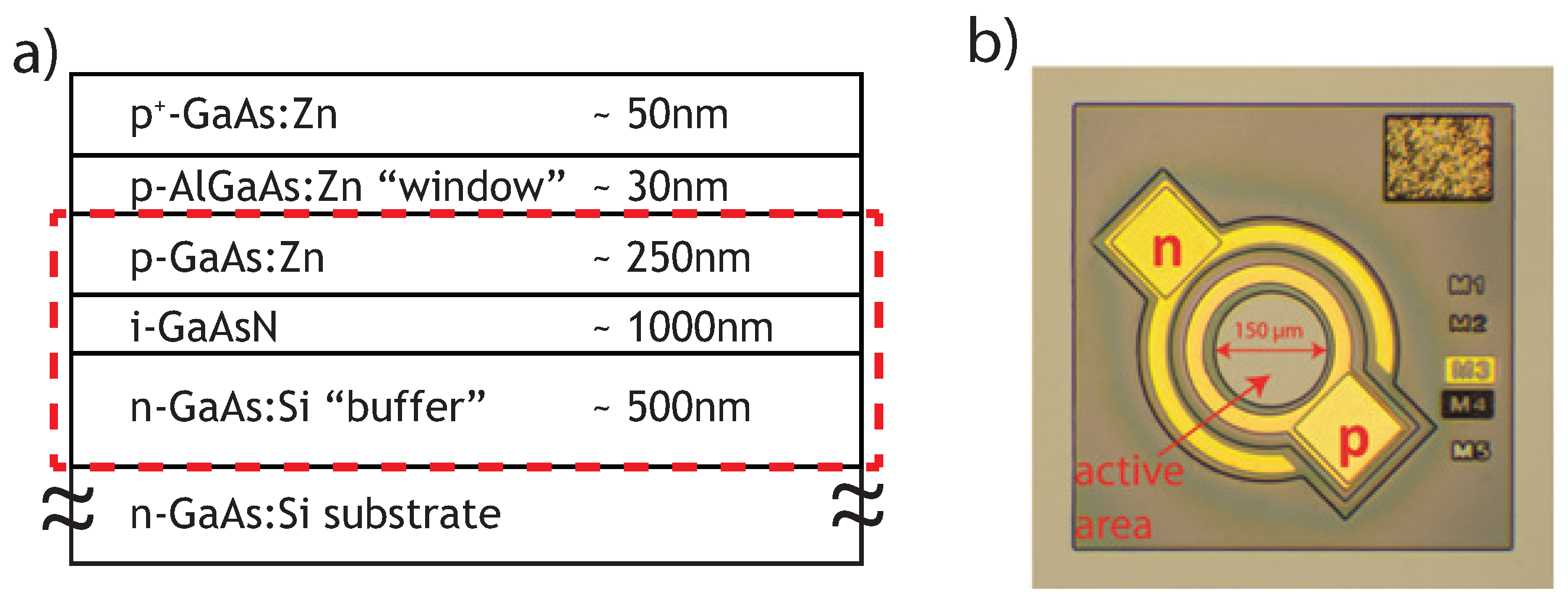
2. Structure Growth and Device Preparation

The investigated structure of dilute nitride GaAsN p-i-n solar cell was grown by the AP-MOVPE method using an AIX 200 R&D horizontal reactor on silicon doped 2″(100) GaAs substrate. Trimethylgallium (TMGa), trimethylaluminium (TMAl), arsine (10% of AsH 3 in H 2 ) and tertiarybutylhydrazine (TBHy) were used as growth precursors, while diethylzinc (DEZn) and silane (20 ppm in H 2 ) were employed as dopant sources. High-purity hydrogen (99.9999%) was used as a carrier gas. The epitaxial structure depicted in Figure 1a consists of a 500 nm thick n-type GaAs buffer, followed by an 800 nm undoped GaAsN base, 250 nm p-type GaAs emitter, thin p-type AlGaAs optical window and 50 nm of a highly doped p-type GaAs contact layer. The growth temperature varied from 575 °C (GaAsN) to 700 °C for AlGaAs and GaAs. GaAsN layers grown in our system exhibit a low electron concentration in the range of 10 16 cm 3 . Detailed growth parameters can be found elsewhere [5,7,16,45].
After growth, the epitaxial structure was divided into smaller parts. One of them was processed to obtain solar cell devices, while the others were ex-situ characterized by different methods, which are mentioned later in the paper. The test solar cell device depicted in Figure 1b is a structure with two planar contacts: p-type Pt/Ti/Pt/Au metal stack deposited on the top of the mesa, defined by the combination of lithography and wet chemical etching and AuGe/Ni/Au n-type contact located at the bottom of the mesa.

3. Experimental Details

Electrical properties, i.e., free electron and hole concentrations across the structure, were investigated by electrochemical capacitance-voltage (EC-V) profiling using BIORAD PN4300 apparatus and a Tiron electrolyte. The structural properties of GaAsN p-i-n solar cell were determined by means of high-resolution X-ray diffraction (HRXRD) using an MRD High Resolution X-Ray Diffractometer. We measured the rocking curve of (004) symmetrical reflex in triple-axis geometry and both symmetrical (004) and asymmetrical (115) reciprocal lattice maps (RLMs). The electrical properties of the fabricated test devices were investigated by means of temperature-dependent current-voltage measurements (J-V-T), using Keithley 237, Keithley 2612A instruments and liquid nitrogen cryostat [43,46], while the light J-V characteristic was measured under AM 1.5 spectrum with sunlight simulator Solar Light 16s-002. DLTFS measurements were carried out using BIORAD DL8000 system in the temperature range from 80 to 550 K of the solar cell structure shown in Figure 1b for the following parameters: time period T W of 0.5 s, filling time t P of 5 ms, reverse voltage V R of −1 V and filling voltage V P of 0.05 V.

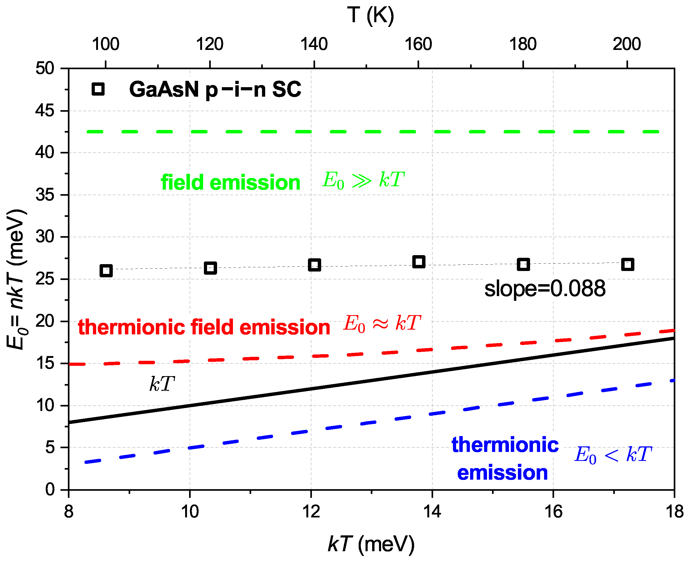
4. Results and Discussion

Epitaxial structure of GaAsN solar cell was investigated by means of electrochemical capacitance-voltage (EC-V) profiling to determine the free carrier profile across the structure and roughly confirm the designed thickness of particular layers shown in Figure 1a. A detailed examination of individual layer thickness and chemical composition was carried out by high-resolution X-ray diffraction (HRXRD) rocking curve measurement. Additionally, we determined the lattice parameters of GaAsN layer and its relaxation by measuring and analyzing reciprocal lattice maps (RLMs) around (004) and (115) points. Electro-optical absorption-like characterization was performed by means of photocurrent spectroscopy (PC) and external quantum efficiency (EQE) measurements. Both methods are able to provide information on the band gap of the material by the analyzing long-wavelength absorption edge. The main characterization method described and discussed in detail in this paper is the temperature-dependent current-voltage (J-V-T) measurement, which provides information about the dominant current transport mechanism through p-i-n junction of the analysed solar cell device. Moreover, J-V-T measurements enable to identify the main generation-recombination centers within the band gap. Finally, we used a powerful deep level transient Fourier spectroscopy (DLTFS) approach for the detection and identification of deep level traps present in the GaAsN base. A detailed description of all the mentioned measurements and their accurate analysis is presented below.

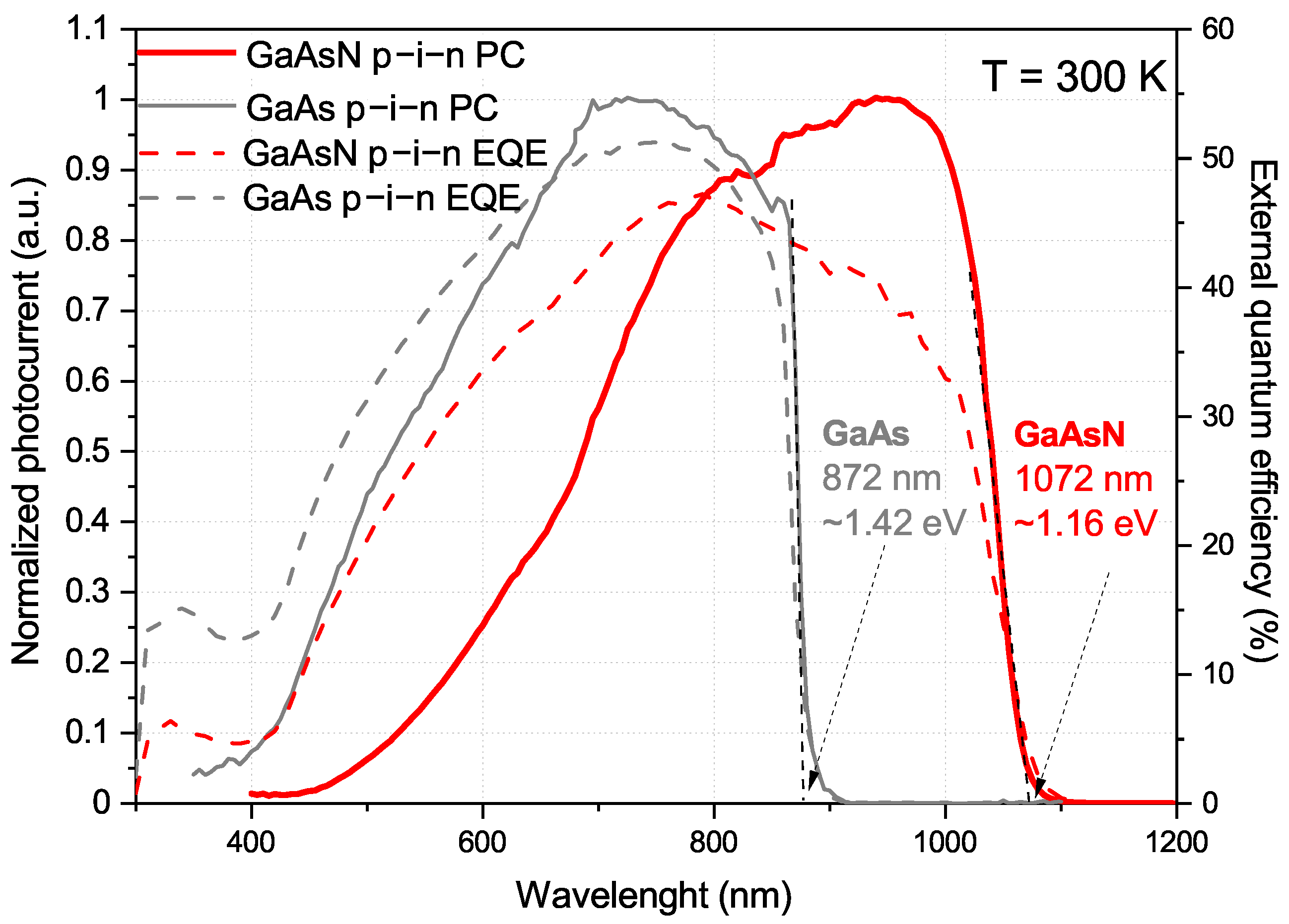
4.1. Electrical and Electro-Optical Characterization

The obtained carrier concentration profile, shown in Figure 2, is in accordance with the scheme of epitaxial structure depicted in Figure 1a: from the left side of the figure, i.e., from the sample surface, a highly Zn-doped p + GaAs:Zn contact layer with holes concentration of 3 × 10 19 cm 3 next p-type AlGaAs:Zn optical window and GaAs:Zn emitter, undoped GaAsN base and, finally, n-type Si-doped GaAs:Si buffer and substrate. The intrinsic carrier concentration in GaAsN base was determined on the basis of depletion C-V measurement taken at the depth of 0.5 μ m, and is shown in the inset in the order of 2–3 × 10 16 cm 3 . The estimated thickness of GaAsN layer (marked here with a dashed rectangle) is about 0.8 μ m.
Band gap energy of the GaAsN base layer was determined using photocurrent (PC) spectroscopy and confirmed by external quantum efficiency measurement (EQE). Both methods are used for the determination of the spectral device response on light illumination; therefore, the analysis of absorption edge provides information about the lowest band gap of the semiconductor structure, in our case, GaAsN. In the case of photocurrent spectroscopy, we obtained information about the current generated under discrete wavelength illumination, while external quantum efficiency defines how many carriers are produced by the absorption of an incident photon of a given energy. In both methods, extrapolation of the absorption edge offers information about the GaAsN base band gap. The obtained spectra are shown in Figure 3, together with the results of the reference GaAs p-i-n solar cell device. The significant redshift in the absorption edge is observable in the GaAsN sample due to the presence of nitrogen. The analysis of photocurrent GaAsN absorption edge yields a band gap of 1.16 eV. According to the Band Anti-Crossing model [12], this energy corresponds to 1.73% of nitrogen content in GaAsN. The EQE results are in accordance with photocurrent spectroscopy and indicate that incident photons in the spectral range of 650–950 nm are absorbed with an efficiency higher than 40%. The relatively low EQE signal of the GaAsN solar cell is probably related to typical dilute nitride material imperfections. The most common disadvantages of GaAsN are its short minority carrier lifetime [26,27], high background doping concentration [8,9] and, finally, the nitrogen-induced defects [4,5,45]. Moreover, the fabrication of anti-reflective coating (not applied on the examined structure) on the solar cell surface should increase the EQE signal [47].
Fabricated GaAsN test solar cells were characterized by J-V measurements under an AM1.5 solar spectrum simulator in order to obtain basic photovoltaic parameters. The typical J–V curve of the test device is shown in Figure 4. We obtained an open-circuit voltage of 0.461 V and short-circuit current density of 21.53 mA/cm 2 , while fill factor and efficiency were equal to 71.97% and 7.11%, respectively. Bouzazi, who investigated a GaAsN-based solar cell, obtained higher V o c = 0.66 V in comparison with our structure, but lower a short-circuit current J s c of 16.52 mA/cm 2 and fill factor of 65%. Finally, both structures, ours and fabricated by Bouzazi have similar efficiencies of 7.11% and 7.10%, respectively [6].

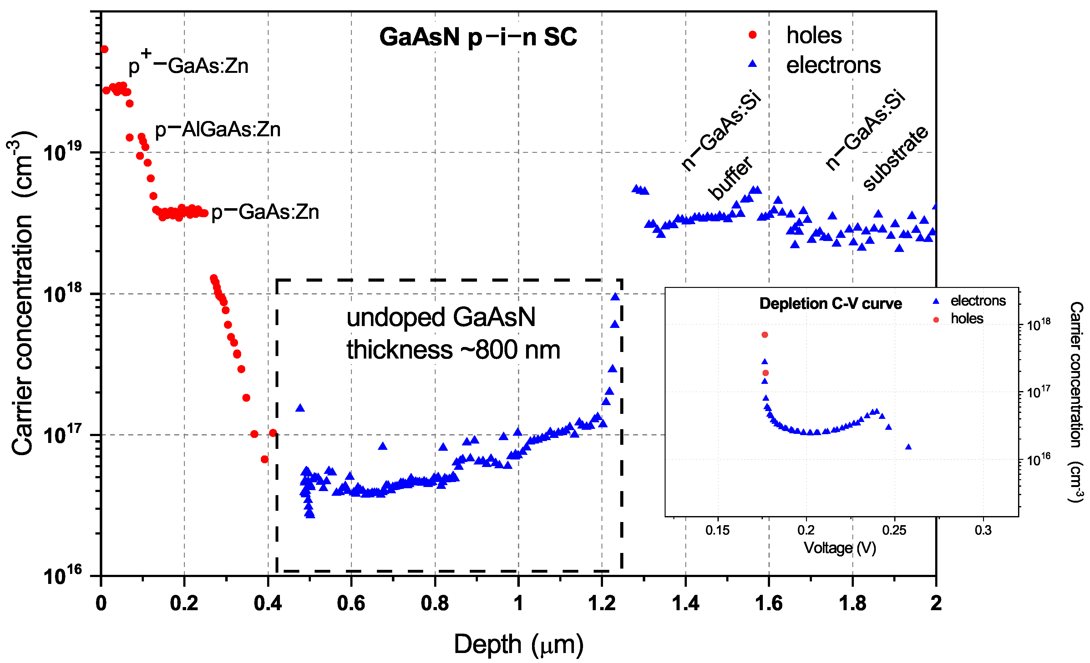
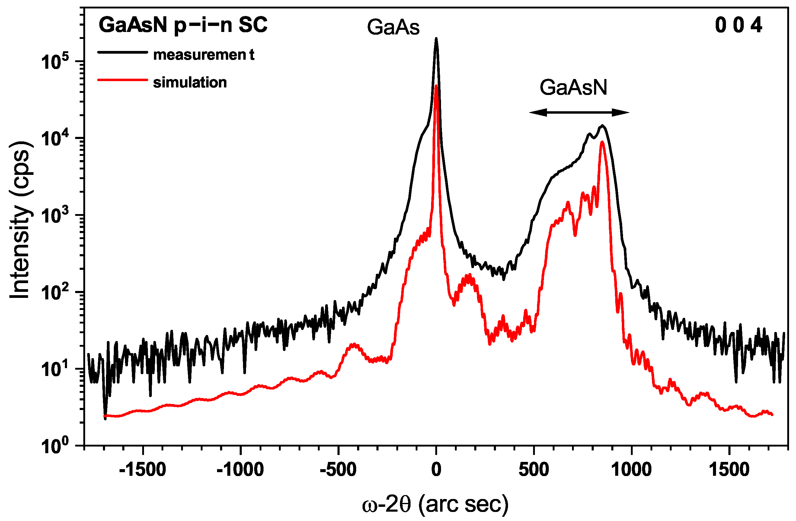
4.2. Structural Characterization

The measured diffraction curve of GaAsN p-i-n solar cell and its simulation are shown in Figure 5.
The highest intensity signal is related to the GaAs substrate; the broadening of this reflex is related to p- and n-type doping of the GaAs layers [48], as well as the presence of a thin AlGaAs optical window layer [49]. The GaAsN signal located on the right side is asymmetrically broadened which might suggest inhomogeneous nitrogen distribution in GaAsN layer. Composition fluctuations in dilute nitride layers such as GaAsN or InGaAsN are well known [16,50,51,52]. Nitrogen has a tendency to form clusters, which, together with N-related defects (for instance, (N-N) A s , (N-As) A s [5,35]), contribute to the formation of non-radiative recombination centers [30] and carrier localization effects [53]. Based on the measured rocking curve of the epitaxial structure of the solar cell, we simulated the composition of the GaAsN base layer using dynamic diffraction theory [54,55]. It consisted of two sublayers with different nitrogen contents (according to the growth direction): the first layer had a thickness of 200 nm with a concavely increasing nitrogen content from 1.2 to 1.67%, and the second one had a thickness of 600 nm and constant N content of 1.67%. The determined nitrogen content is in good agreement with the calculations according to the BAC model, while GaAsN thickness is in accordance with the EC-V findings. The 50 nm thick optical window layer composition was determined to be Al 0.5 Ga 0.5 As.
The inhomogeneous composition of the GaAsN layer was also confirmed by reciprocal lattice mapping. A map of the symmetric Miller reflection plane (004) shown in Figure 6a reveals a broad and high intensity peak related to GaAs. The diffusive scattering is present around (004) GaAs reciprocal lattice point (RLP), and plotted as line scans number 1 and 3 in Figure 6a insets, elongated along the Q x axis (FWHM along Q x of 0.00033 Å 1 , while FWHM Q z = 0.00028 Å 1 ) is related to the crystal imperfection induced by zinc and silicon doping of GaAs layers [56,57].
Another explanation for the broad signal related to GaAs is the presence of a highly doped AlGaAs optical widow layer grown at the higher temperature of 700 °C. Diffusive scattering around GaAsN RLP (line scans number 2 and 3) has a more isotropic shape, i.e., we can observe comparable broadening along Q x and Q z axes: 0.00042 Å 1 for FWHM Q x and FWHM Q z = 0.000383 Å 1 , respectively. However, the elongation in the lengthwise Q z direction is asymmetrical—in other words, the GaAsN-related signal is stretched more to GaAs, in accordance with the rocking curve scan depicted in Figure 2. These findings confirm that the nitrogen composition of GaAsN layer is not homogeneous.
An asymmetrical RLM of around (115) reflection is depicted in Figure 3b, where red dashed lines (diagonal and vertical) indicate the expected signal positions for fully relaxed and completely strained layers, respectively. A high-intensity signal related to the GaAs layer is located at the intersection of these lines, whereas the GaAsN peak is almost located at the full strain line. This indicates that, in the case of the thick GaAsN layer, the relaxation level is very low (about 5.5%), most probably due to non-uniform nitrogen content in the GaAsN layer. The calculated critical thickness of the GaAsN layer with a lower N content of 1.2% according to the Matthews–Blakeslee model [58,59] is about 130–150 nm, while the total thickness of the GaAsN layer is five-fold thicker, i.e., 0.8 μ m. It appears that the presence of a 200 nm thick GaAsN sublayer with gradual nitrogen concentration suppresses the relaxation process of the whole GaAsN absorber.
Based on RLM analysis, the GaAsN lattice parameters were determined to be a of 5.6499 Å, while a of 5.6182 Å. The value of the in-plane a parameter is close to the GaAs lattice constant of a = 5.6533 Å, indicating that the GaAsN unit cell is under biaxial tensile stress [60]. The a parameter for the fully relaxed GaAsN layer, calculated according to Vegard’s law [28], is 5.6347 Å, which confirms the slight relaxation of our layer. However, the lattice unit in the perpendicular direction, a , is directly related to the nitrogen content in the layer, and is in accordance with a = f ( % N ) dependency, as presented by Uesugi for Metal Organic Molecular Beam Epitaxy (MOMBE)-grown GaAsN layers [29].

4.3. Temperature-Dependent Current-Voltage Characterization

J-V-T technique provides information about the presence of generation-recombination centers within the band gap and quality of contacts [6]. Here, we focused only on the dark J-V-T characteristics measured in the range 100–380 K with 20 K step, which are depicted in Figure 7.
Generally, current transport through the p-n or p-i-n junction is governed by various physical phenomena such as diffusion, recombination, thermionic field emission or tunnelling [38,39,40,41,42,43,44]. Precise analysis of temperature-dependent J-V characteristics allows for identification of the dominant mechanism responsible for charge carrier transport. Such investigations have been successfully performed for different types of solar cell devices [39,40,42,43,61,62,63,64,65], metal-semiconductor Schottky diodes [38,66,67,68,69,70,71], semiconductor heterojunction [44,72,73,74], as well as lasers [41] and light-emitting diodes [75]. Using a general diode model, the current–voltage relationship is as follows [39,42]:
J ( V , T ) = J 0 ( T ) [ e x p A ( T ) V 1 ] ,
where J 0 is a saturation current density and A is a pre-exponential fitting parameter defined as:
A = q n k T .
By precise monitoring of the temperature evolution of both the saturation current J 0 and A factor, we are able to draw conclusions about the current flow mechanism under forward bias. As both J 0 and factor A (as well as n related to A by Equation (2)) exhibit different temperature behaviours, governed by the carrier transport model, we collected thermal dependencies of J 0 , A and n in Table 2.
In ideal p-n or p-i-n junction carrier transport is dominated by a diffusion process, where J 0 is thermally activated with E a equal to the material band gap, temperature-dependent pre-exponential parameter A = q k T and ideality factor n of 1 [42,76]. If the dominant current transport mechanism is recombination, factor A changes with temperature, J 0 slope yields thermal activation energy equal to half of the material band gap and the n factor is close to 2 [39,76]. In the case of the p-i-n junction, where the thermionic emission is a dominating mechanism, the junction can be analysed as a Schottky diode with ideality factor n of 1 [44]. When the junction current has a tunnelling nature, the A pre-exponential parameter is temperature-independent (i.e., has an almost constant value) and current is related with E 0 characteristic tunnelling energy [66]. One of the mentioned mechanisms may dominate the others at a certain temperature or voltage region.
The values of pre-exponential factor A were determined by the linear approximation of measured J-V characteristics with Equation (1), and plotted versus reciprocal temperature (1000/T) in Figure 8a. The behaviour of A is nonlinear—however, we are able to divide A factor changes into two smaller regions: high temperature (HT) from 200 to 380 K and low temperature (LT) from 100 to 200 K. We observe the linear increase in A at the HT region, as confirmed by a large (more than six) slope of the fitting line, which may suggest that recombination is a dominant mechanism of current flow. At the LT region, we obtained the almost constant value of A for the analysed solar cell (slope of the fitting line close to zero). The insensitivity of A to temperature changes might indicate that tunnelling is responsible for current transport in LT region.
According to Equation (2), we determined the ideality factor n values for solar cell devices. The temperature evolution of n is shown in Figure 8b. In the HT region, n varies in the range from 1.29 to 1.55, while in the LT region, ideality factor linearly increases as the temperature lowers, reaching 3.01 at 100 K. The increase in ideality factor with the decrease in temperature is a well-known phenomenon related to thermionic emission [77,78]. Han et al. investigated MBE-grown single-junction GaAs solar cell by means of J-V measurements in the 100–400 K temperature range. They determined the ideality factors of 4.38 and 1.7 at 100 K and 300 K, respectively [79]. Alburaih investigated the influence of post-growth annealing on the properties of MBE-grown dilute nitride GaAsNP diodes. He noticed that ideality n decreases from 6.8 at 110 K to 1.99 at 300 K for the as-grown diode, while, for the annealed one, the n drops from 6.3 at 100 K to 2.7 at 300 K [78]. In CdTe-based solar cells, Fiat et al. obtained an n of 5.43 at 80 K; then, n decreased to 1.4 at 300 K [80]. Uslu analysed the J-V-T characteristics of single-quantum well GaAs/AlGaAs laser structure and, at 80 K, obtained an ideality factor of 3.49, while, at 290 K, n decreased to 1.804 [41]. Özavci for Au/GaAs Schottky diodes obtain an ideality factor of 5.43 at 80 K and 1.4 for room-temperature [81]. In all the aforementioned cases, authors connected high values of n at the LT region with a thermionic emission.
In Figure 8c, we plotted the saturation current density J 0 dependency on 1000 / T for an investigated GaAsN solar cell. By analysis of J 0 evolution with reciprocal temperature, we were able to distinguish a region where J 0 changes were fitted by linear function. The inclination of the Arrhenius curve was then recalculated using equation [42,43]:
J 0 e x p E a k T
to obtain the thermal activation energy E a . An energy E a of 0.667 eV was obtained. This level, located near the mid-gap of 1.16 eV GaAsN base layer (0.667 eV below conduction band edge and 0.493 eV above valence band edge), is deep enough to contribute to the current flow of the solar cell.
The analysis of dark J-V-T characteristics and, therefore, temperature-dependent parameters of A, n and J 0 , reveals that their changes with temperature in HT region follow the rule of recombination as a dominant carrier transport mechanism, which takes place via the trap located 0.667 eV below the conduction band edge.
As the pre-exponential factor A is almost temperature-independent (i.e., the slope of the fitting line is very small) and the ideality factor n linearly increases with reciprocal temperature, the conduction mechanism in LT region is probably governed by quantum mechanical tunnelling. To verify this assumption, we plotted, in Figure 9, a relation of n k T versus k T with three theoretical dependencies, whose inclinations represent different current flow mechanisms at low temperature: thermionic emission (TE), field emission (FE) and thermionic field emission (TFE) [66].
Taking the relation shown in Figure 9 and temperature changes in n depicted in Figure 8b into account, as well as the current mechanism rules listed in Table 2, we were able to neglect thermionic emission as a main current flow mechanism at LT region because there was not a constant value of n. To decide between FE and TFE, we analysed the equation related to tunnelling current listed in Table 2 [38,41,66,82]:
J 0 e x p q V E 0 ,
where E 0 is defined as:
E 0 = n k T q = E 00 coth q E 00 k T ,
and E 00 is a characteristic tunnelling energy. Based on Equation (5), the values of E 0 were calculated and plotted together with theoretical dependencies in Figure 9. If the field emission governs the current flow, E 00 is temperature-independent and equal to E 0 [81]. Moreover, its value is significantly higher than k T (black line in Figure 9) [66]. For instance, Bayhan investigated ZnO/CdS/Cu(In,Ga)Se 2 solar cell and determined E 0 to be 129.4 meV [61], while Arslan obtained 85.7 meV for AlGaN/AlN/GaN heterostructures [83]. Tecimer got E 0 of 87 meV for PVA:Zn/n-GaAs Schottky diodes [68]. Filali, who analysed AlGaAs/GaAs/AlGaAs Schottky diodes, determined E 0 of 65 to 70 meV for the temperature range of 80–200 K [38]. In all the aforementioned examples, the main current transport mechanism was assigned as field emissions.
In our case, the determined E 0 energies are significantly lower: 26.21 meV at 100 K, and slightly increase with temperature to 26.91 meV at 200 K (slope of the fitting line equal to 0.088). At the lowest temperature of 100 K, the E 0 is greater than k T —furthermore, with a temperature increase, this difference ( E 0 - k T ) drops, meaning that the tunnelling current dominates at low temperatures, and its contribution decreases when T rises. Similar findings were reported by Uslu, who investigated transport mechanisms in a GaAs/AlGaAs quantum well laser and obtained E 0 values of from 24 to 26 meV in the temperature range from 80 to 170 K [41]. Kim focused his research on a GaAs solar cell with InAs quantum dots (QD) and determined the tunnelling characteristic energy to be 24 and 18 meV for structure with quantum dots and reference without QD [65]. In the case of Au/n-GaAs Schottky barrier diodes investigated by Özavcı, a tunnelling characteristic energy of 28.04 meV was determined, while the transport mechanism was assigned to TFE [81]. The E 0 determined for our structures and k T have similar values to those already reported by Uslu [41], Kim [65] or Özavcı [81]. On the other hand, E 0 are greater than k T which excludes TE, furthermore determined E 0 are too small for assignment current transport mechanism as a field emission. Therefore, we believe that, in the case of our GaAsN-based solar cell, the dominant mechanism at LT region is thermionic field emission.

4.4. Deep Level Transient Fourier Spectroscopy Investigations

To verify the presence of a deep level near the mid-gap of GaAsN ( E a of 0.667 eV determined from J-V-T measurements), we employed the powerful deep level transient spectroscopy (DLTS) method used for semiconductor material defect characterization, first described by Lang in 1974 [84]. The main energy level parameters that can be obtained by evaluation of the DLTS measurements are deep level (trap) activation energy ( E T ) and capture cross-section ( σ T ). They describe the energy state of the deep level that can be visually described in the forbidden gap in the energy band diagram of the semiconductor. The sign of each peak indicates whether the observed defect acts as a trap for minority or majority carriers, while the measured capacitance is proportional to defect concentration. DLTS-based methods are very efficient in defect determination in different semiconductor materials and devices, such as diodes [85,86], Schottky diodes [68,69] and rectifiers [87,88], solar cells [5,89,90], bipolar [91] and HEMT transistors [92] or laser structures [93,94]. A digital modification of DLTS, the deep level transient Fourier spectroscopy (DLTSFS) method measures the complete capacitance transient as a C ( t ) array and transfers the data into a computer system. Using a Fourier transformation and direct evaluation, the time constant and the transient amplitude can be evaluated for every transient measured, at any temperature. In the DLTFS approach used within this study, the separation of overlapped defects, extending the conventional rate window, as well as the adjustment of capacitance transients with scanned sampling intervals, are possible [95].
The detailed measurement conditions can be found elsewhere [5,45,96]. A typical DLTFS spectrum of the GaAsN solar cell structure is presented in Figure 10a, where the positive value of measured capacitance signal indicates that the detected deep levels in GaAsN structure are majority carrier (electron) traps.
The capacitance signal was analysed using a deconvolution algorithm in order to identify defects. A reverse spectra fitting procedure was employed for verification of the convergence between measured and calculated data. As a result of the aforementioned operations, we obtained capacitance signals of individual traps, labelled here as AT1 to AT8, which are depicted with different colours in Figure 10a. The light green line represents the sum of determined signals and fits very well to the measured data. Based on deconvoluted capacitance transients, we calculated Arrhenius curves, which are plotted in Figure 10b. These dependencies enable us to calculate the trap energy E C E T and capture the cross-section σ T of the defects, which are collected in Table 3 together with the probable origin, assumed after comparison with the literature.
The dominant trap, i.e., the one with the highest capacitance signal (AT4 in Figure 10a) and energy of 0.670 eV, was assigned as the nitrogen dimer on an arsenic site (N-N) A s , i.e., two nitrogen atoms in the place of arsenic, which is a typical defect for dilute nitrides [31,32,33,99]. Based on the information of intrinsic GaAsN carrier concentration in the order of 2–3 × 10 16 cm 3 , we roughly estimated the N T concentration to be 1.16 × 10 15 cm 3 . The nitrogen split interstitial defect was reported by many groups with an energy of 0.6 eV [33], 0.62 eV [34], 0.644 eV to 0.692 eV [45], 0.65 to 0.67 eV [35], 0.66 eV [32], or even 0.8 eV [99] above the valence band edge or below the conduction band egde, depending on the intrinsic conductivity type of GaAsN. In general, nitrogen interstitial (N-N) acts as a carrier trapping and scattering centre [100], which could be partially removed by rapid thermal annealing [31,99,101,102]. According to the works of Li and Zhang, during the GaAsN growth, the formation of N-N interstitials is energetically favourable in comparison with other nitrogen-related defects: N-As interstitials [28,32]. Arola calculated that energies of N-N interstitial defects (on both Ga or As site) are significantly lower per N atom than energies for single nitrogen on the Ga and As site [103]. Moreover, (N-N) A s defects partially reduce the lattice strain introduced by arsenic substitution with nitrogen atoms [28,31]. The other detected traps seem to be the typical defects of GaAs-related materials, and were identified in accordance with the work of Martin [97] and Lang [98].
Please note that the dominant deep-level AT4 observed in our GaAsN solar cell, and identified here as nitrogen interstitial, has an energy E T of 0.670 eV. This value coincides with the E a value of 0.667 eV, determined on the basis of J-V-T measurements. These findings clearly confirm that, in the HT region, the current transport mechanism is recombination via mid-gap trap with an energy of circa 0.670 eV below the conduction band edge.
To date, to the best of our knowledge, only one paper deals with current transport mechanism investigation in a dilute nitride GaAsN-based p-n solar cell. Bouzazi grew, fabricated and characterized a GaAsN homojunction device with a nitrogen content of 0.73% using chemical beam epitaxy [6]. Their structure after growth was in situ annealed at 500 °C for 1 h. The analysis of J-V-T measurement results, in the range of from 200 to 300 K, confirmed that the recombination current in the GaAsN p-n junction is connected with a defect level at 0.31 eV. DLTS results identified two defects in the GaAsN layer with energies of 0.33 and 0.69 eV below the conduction band edge, which were assigned as nitrogen-related defects and EL2—native GaAs trap. The aforementioned N-related deep level was N-As interstitial, i.e., an arsenic–nitrogen pair on the arsenic site. Bouzazi, as well us, within this paper, related the recombination character of current flow with the presence of a N-related trap within the GaAsN band gap. However, Bouzazi found (N-As) A s in an annealed sample, while we identified (N-N) A s in an as-grown structure, in accordance with previously published papers where the transformation of (N-N) A s into (N-As) A s was reported [31,99,101,102].

5. Conclusions

In sum, the electro-optical and structural properties of GaAsN solar cells were studied and analysed in detail. Our findings indicate that a 0.8 μ m thick GaAsN base layer is practically strained (5.5% of relaxation was determined by RLM analysis), despite its nitrogen content of 1.67%. Therefore, we believe that the unintentional gradual N composition in the first 200 nm of GaAsN sublayer suppresses crystal relaxation, which, in turn, enables it to exceed the critical thickness limitation without causing a deterioration of structural properties. Both absorption-like measurement methods (PC and EQE) indicate an absorption edge of 1072 nm, corresponding to an energy of 1.16 eV for the GaAsN base layer. Temperature-dependent current-voltage characterization points to the presence of a mid-gap trap with thermal activation energy E a of 0.667 eV. A detailed analysis of general diode model parameters, i.e., pre-exponential coefficient A, ideality factor n and saturation current density J 0 , assigned the recombination process as a dominant current flow mechanism at temperatures above 200 K. Moreover, the identified trap with energy 0.667 eV acts as a recombination center for electrons. In the LT region, i.e., from 100 to 200 K, the current mechanism was identified as a thermionic field emission with tunnelling energies E 0 of from 26.21 to 26.91 meV for 100 and 200 K, respectively. The DLTFS investigation revealed several deep levels in our GaAsN solar cell structure, among which the most dominant was a trap with an activation energy of 0.670 eV. This defect is the same as the mid-gap energy state determined by J-V-T analysis. Based on the literature review and DLTFS system database, we assigned it to nitrogen interstitials, i.e., (N-N) A s . This unambiguously confirms that nitrogen-related defects act as a recombination centre and, therefore, have a significant impact on current flow mechanisms in the temperature range of from 200 to 380 K.

Author Contributions

Conceptualization, W.D., M.M., L.S. and B.Ś.; Funding acquisition, W.D., M.M., L.S. and B.Ś.; Investigation, W.D., K.B., M.M., J.D., J.S., I.L., D.R., W.K., A.K., M.F., J.K.J., C.A., L.S. and B.Ś.; Methodology, W.D., K.B., M.M., L.S. and B.Ś.; Project administration, W.D. and B.Ś.; Visualization, W.D., K.B., M.M., I.L., M.F. and L.S.; Writing—original draft, W.D., L.S. and B.Ś. All authors have read and agreed to the published version of the manuscript.

Funding

This work was co-financed by the Polish National Agency for Academic Exchange under the contract number PPN/BIL/2018/1/00137/U/00001, by Wrocław University of Science and Technology subsidy, by Scientific Grant Agency of the Ministry of Education of the Slovak Republic (VEGA 1/0733/20) and Slovak Research and Development Agency (project SK-PL-18-0068 and APVV-17-0169).

Institutional Review Board Statement

Not applicable.

Informed Consent Statement

Not applicable.

Data Availability Statement

Data available on request from corresponding author.

Acknowledgments

This work was accomplished thanks to the product indicators and result indicators achieved within the projects co-financed by the European Union within the European Regional Development Fund, through a grant from the Innovative Economy (POIG.01.01.02-00-008/08-05) and by the National Centre for Research and Development through the Applied Research Program Grant No. 178782 and Grant LIDER No. 027/533/L-5/13/NCR/2014.B.

Conflicts of Interest

The authors declare no conflict of interest.

References

  1. Bank, S.R.; Bae, H.; Goddard, L.L.; Yuen, H.B.; Wistey, M.A.; Kudrawiec, R.; Harris, J.S. Recent Progress on 1.55-μm Dilute-Nitride Lasers. IEEE J. Quantum Electron. 2007, 43, 773–785. [Google Scholar] [CrossRef]
  2. Tansu, N.; Yeh, J.Y.; Mawst, L. High-performance 1200-nm InGaAs and 1300-nm InGaAsN quantum-well lasers by metalorganic chemical vapor deposition. IEEE J. Sel. Top. Quantum Electron. 2003, 9, 1220–1227. [Google Scholar] [CrossRef]
  3. Tomic, S.; O’Reilly, E.; Fehse, R.; Sweeney, S.; Adams, A.; Andreev, A.; Choulis, S.; Hosea, T.; Riechert, H. Theoretical and experimental analysis of 1.3-μm InGaAsN/GaAs lasers. IEEE J. Sel. Top. Quantum Electron. 2003, 9, 1228–1238. [Google Scholar] [CrossRef]
  4. Polojärvi, V.; Aho, A.; Tukiainen, A.; Raappana, M.; Aho, T.; Schramm, A.; Guina, M. Influence of As/group-III flux ratio on defects formation and photovoltaic performance of GaInNAs solar cells. Sol. Energy Mater. Sol. Cells 2016, 149, 213–220. [Google Scholar] [CrossRef]
  5. Kosa, A.; Stuchlikova, L.; Harmatha, L.; Mikolasek, M.; Kovac, J.; Sciana, B.; Dawidowski, W.; Radziewicz, D.; Tlaczala, M. Defect distribution in InGaAsN/GaAs multilayer solar cells. Sol. Energy 2016, 132, 587–590. [Google Scholar] [CrossRef]
  6. Bouzazi, B.; Kojima, N.; Ohshita, Y.; Yamaguchi, M. Analysis of Current Transport Mechanisms in GaAsN Homojunction Solar Cell Grown by Chemical Beam Epitaxy. IEEE J. Photovoltaics 2013, 3, 909–915. [Google Scholar] [CrossRef]
  7. Dawidowski, W.; Ściana, B.; Zborowska-Lindert, I.; Mikolášek, M.; Kováč, J.; Tłaczała, M. Tunnel junction limited performance of InGaAsN/GaAs tandem solar cell. Sol. Energy 2021, 214, 632–641. [Google Scholar] [CrossRef]
  8. Jackrel, D.B.; Bank, S.R.; Yuen, H.B.; Wistey, M.A.; Harris, J.S.; Ptak, A.J.; Johnston, S.W.; Friedman, D.J.; Kurtz, S.R. Dilute nitride GaInNAs and GaInNAsSb solar cells by molecular beam epitaxy. J. Appl. Phys. 2007, 101, 114916. [Google Scholar] [CrossRef] [Green Version]
  9. Miyashita, N.; Ahsan, N.; Okada, Y. Generation and collection of photocarriers in dilute nitride GaInNAsSb solar cells. Prog. Photovoltaics Res. Appl. 2016, 24, 28–37. [Google Scholar] [CrossRef]
  10. Milanova, M.; Donchev, V.; Cheetham, K.J.; Cao, Z.; Sandall, I.; Piana, G.M.; Hutter, O.S.; Durose, K.; Mumtaz, A. Single-junction solar cells based on p-i-n GaAsSbN heterostructures grown by liquid phase epitaxy. Sol. Energy 2020, 208, 659–664. [Google Scholar] [CrossRef]
  11. Gonzalo, A.; Stanojević, L.; Fuertes Marrón, D.; Guzman, A.; Hierro, A.; Ulloa, J. 1 eV GaAsSbN–based solar cells for efficient multi-junction design: Enhanced solar cell performance upon annealing. Sol. Energy 2021, 221, 307–313. [Google Scholar] [CrossRef]
  12. Shan, W.; Walukiewicz, W.; Ager, J.W.; Haller, E.E.; Geisz, J.F.; Friedman, D.J.; Olson, J.M.; Kurtz, S.R. Band Anticrossing in GaInNAs Alloys. Phys. Rev. Lett. 1999, 82, 1221–1224. [Google Scholar] [CrossRef]
  13. Su, M.; Li, C.; Yuan, P.; Rao, F.; Jia, Y.; Wang, F. Electronic and optical properties of quaternary alloy GaAsBiN lattice-matched to GaAs. Opt. Express 2014, 22, 30633–30640. [Google Scholar] [CrossRef]
  14. Occena, J.; Jen, T.; Mitchell, J.W.; Linhart, W.M.; Pavelescu, E.M.; Kudrawiec, R.; Wang, Y.Q.; Goldman, R.S. Mapping the composition-dependence of the energy bandgap of GaAsNBi alloys. Appl. Phys. Lett. 2019, 115, 082106. [Google Scholar] [CrossRef]
  15. Wang, L.; Zhang, L.; Yue, L.; Liang, D.; Chen, X.; Li, Y.; Lu, P.; Shao, J.; Wang, S. Novel Dilute Bismide, Epitaxy, Physical Properties and Device Application. Crystals 2017, 7, 63. [Google Scholar] [CrossRef]
  16. Ściana, B.; Radziewicz, D.; Dawidowski, W.; Bielak, K.; Szyszka, A.; Kopaczek, J. Impact of gallium concentration in the gas phase on composition of InGaAsN alloys grown by AP-MOVPE correlated with their structural and optical properties. J. Mater. Sci. Mater. Electron. 2021, 30, 16216–16225. [Google Scholar] [CrossRef] [Green Version]
  17. Bian, L.; Jiang, D.; Tan, P.; Lu, S.; Sun, B.; Li, L.; Harmand, J. Photoluminescence characteristics of GaAsSbN/GaAs epilayers lattice-matched to GaAs substrates. Solid State Commun. 2004, 132, 707–711. [Google Scholar] [CrossRef]
  18. Richards, R.; Mellor, A.; Harun, F.; Cheong, J.; Hylton, N.; Wilson, T.; Thomas, T.; Roberts, J.; Ekins-Daukes, N.; David, J. Photovoltaic characterisation of GaAsBi/GaAs multiple quantum well devices. Sol. Energy Mater. Sol. Cells 2017, 172, 238–243. [Google Scholar] [CrossRef]
  19. Gaddy, E.M. Cost trade between multijunction, gallium arsenide and silicon solar cells. Prog. Photovoltaics Res. Appl. 1996, 4, 155–161. [Google Scholar] [CrossRef]
  20. Aho, A.; Isoaho, R.; Tukiainen, A.; Gori, G.; Campesato, R.; Guina, M. Dilute nitride triple junction solar cells for space applications: Progress towards highest AM0 efficiency. Prog. Photovoltaics Res. Appl. 2018, 26, 740–744. [Google Scholar] [CrossRef]
  21. Sabnis, V.; Yuen, H.; Wiemer, M. High-efficiency multijunction solar cells employing dilute nitrides. AIP Conf. Proc. 2012, 1477, 14–19. [Google Scholar] [CrossRef] [Green Version]
  22. Núñez, N.; Vázquez, M.; González, J.R.; Jiménez, F.J.; Bautista, J. Instrumentation for accelerated life tests of concentrator solar cells. Rev. Sci. Instrum. 2011, 82, 024703. [Google Scholar] [CrossRef] [PubMed] [Green Version]
  23. Herb, J. Commercialization of New Lattice-Matched Multi-Junction Solar Cells Based on Dilute Nitrides: July 8, 2010–March 7, 2012; National Renewable Energy Lab. (NREL): Golden, CO, USA, 2012. [Google Scholar]
  24. Suarez, F.; Liu, T.; Sukiasyan, A.; Lang, J.; Pickett, E.; Lucow, E.; Bilir, T.; Chary, S.; Roucka, R.; Aeby, I.; et al. Advances in Dilute Nitride Multi-Junction Solar Cells for Space Power Applications. E3S Web Conf. 2017, 16, 03006. [Google Scholar] [CrossRef]
  25. Volz, K.; Stolz, W.; Teubert, J.; Klar, P.J.; Heimbrodt, W.; Dimroth, F.; Baur, C.; Bett, A.W. Doping, Electrical Properties and Solar Cell Application of GaInNAs. In Dilute III-V Nitride Semiconductors and Material Systems: Physics and Technology; Erol, A., Ed.; Springer: Berlin/Heidelberg, Germany, 2008; pp. 369–404. [Google Scholar] [CrossRef]
  26. Kim, T.; Wood, A.; Kim, H.; Kim, Y.; Lee, J.; Peterson, M.; Sin, Y.; Moss, S.; Kuech, T.F.; Babcock, S.; et al. Impact of Sb Incorporation on MOVPE-Grown “Bulk” InGaAs(Sb)N Films for Solar Cell Application. IEEE J. Photovoltaics 2016, 6, 1673–1677. [Google Scholar] [CrossRef]
  27. Kim, T.; Forghani, K.; Mawst, L.; Kuech, T.; LaLumondiere, S.; Sin, Y.; Lotshaw, W.; Moss, S. Properties of ‘bulk’ GaAsSbN/GaAs for multi-junction solar cell application: Reduction of carbon background concentration. J. Cryst. Growth 2014, 393, 70–74. [Google Scholar] [CrossRef]
  28. Li, W.; Pessa, M.; Likonen, J. Lattice parameter in GaNAs epilayers on GaAs: Deviation from Vegard’s law. Appl. Phys. Lett. 2001, 78, 2864–2866. [Google Scholar] [CrossRef]
  29. Uesugi, K.; Morooka, N.; Suemune, I. Reexamination of N composition dependence of coherently grown GaNAs band gap energy with high-resolution x-ray diffraction mapping measurements. Appl. Phys. Lett. 1999, 74, 1254–1256. [Google Scholar] [CrossRef] [Green Version]
  30. Gao, Q.; Tan, H.; Jagadish, C.; Sun, B.; Gal, M.; Ouyang, L.; Zou, J. Metalorganic chemical vapor deposition of GaAsN epilayers: Microstructures and optical properties. J. Cryst. Growth 2004, 264, 92–97. [Google Scholar] [CrossRef]
  31. Gelczuk, L.; Stokowski, H.; Dąbrowska-Szata, M.; Kudrawiec, R. Origin and annealing of deep-level defects in GaNAs grown by metalorganic vapor phase epitaxy. J. Appl. Phys. 2016, 119, 185706. [Google Scholar] [CrossRef]
  32. Zhang, S.B.; Wei, S.H. Nitrogen Solubility and Induced Defect Complexes in Epitaxial GaAs:N. Phys. Rev. Lett. 2001, 86, 1789–1792. [Google Scholar] [CrossRef] [PubMed]
  33. Shafi, M.; Mari, R.; Henini, M.; Taylor, D.; Hopkinson, M. Electrical properties of nitrogen-related defects in n-type GaAsN grown by molecular-beam epitaxy. Phys. Status Solidi C 2009, 6, 2652–2654. [Google Scholar] [CrossRef]
  34. Yamaguchi, M.; Ohshita, Y.; Kojima, N.; Suzuki, H.; Bouzazi, B. Analysis of defects and impurities in new (In)GaAsN materials for concentrator multi-junction solar cells. In Proceedings of the 2009 34th IEEE Photovoltaic Specialists Conference (PVSC), Philadelphia, PA, USA, 7–12 June 2009; pp. 2332–2335. [Google Scholar] [CrossRef]
  35. Dhar, S.; Halder, N.; Mondal, A.; Bansal, B.; Arora, B.M. Detailed studies on the origin of nitrogen-related electron traps in dilute GaAsN layers grown by liquid phase epitaxy. Semicond. Sci. Technol. 2005, 20, 1168–1172. [Google Scholar] [CrossRef]
  36. García, I.; Ochoa, M.; Lombardero, I.; Cifuentes, L.; Hinojosa, M.; Caño, P.; Rey-Stolle, I.; Algora, C.; Johnson, A.; Davies, I.; et al. Degradation of subcells and tunnel junctions during growth of GaInP/Ga(In)As/GaNAsSb/Ge 4-junction solar cells. Prog. Photovoltaics Res. Appl. 2017, 25, 887–895. [Google Scholar] [CrossRef] [Green Version]
  37. Rey-Stolle, I.; García, I.; Barrigón, E.; Olea, J.; Pastor, D.; Ochoa, M.; Barrutia, L.; Algora, C.; Walukiewicz, W. On the thermal degradation of tunnel diodes in multijunction solar cells. AIP Conf. Proc. 2017, 1881, 040005. [Google Scholar] [CrossRef] [Green Version]
  38. Filali, W.; Sengouga, N.; Oussalah, S.; Mari, R.H.; Jameel, D.; Al Saqri, N.A.; Aziz, M.; Taylor, D.; Henini, M. Characterisation of temperature dependent parameters of multi-quantum well (MQW) Ti/Au/n-AlGaAs/n-GaAs/n-AlGaAs Schottky diodes. Superlattices Microstruct. 2017, 111, 1010–1021. [Google Scholar] [CrossRef]
  39. Schulze, T.F.; Korte, L.; Conrad, E.; Schmidt, M.; Rech, B. Electrical transport mechanisms in a-Si:H/c-Si heterojunction solar cells. J. Appl. Phys. 2010, 107, 023711. [Google Scholar] [CrossRef]
  40. Wilhelm, H.; Schock, H.W.; Scheer, R. Interface recombination in heterojunction solar cells: Influence of buffer layer thickness. J. Appl. Phys. 2011, 109, 084514. [Google Scholar] [CrossRef]
  41. Uslu, H.; Bengi, A.; Çetin, S.; Aydemir, U.; Altındal, S.; Aghaliyeva, S.; Özçelik, S. Temperature and voltage dependent current-transport mechanisms in GaAs/AlGaAs single-quantum-well lasers. J. Alloy. Compd. 2010, 507, 190–195. [Google Scholar] [CrossRef]
  42. Marsal, L.F.; Martin, I.; Pallares, J.; Orpella, A.; Alcubilla, R. Annealing effects on the conduction mechanisms of p+-amorphous- Si0.8C0.2:H/n-crystalline-Si diodes. J. Appl. Phys. 2003, 94, 2622–2626. [Google Scholar] [CrossRef]
  43. Mikolášek, M.; Nemec, M.; Vojs, M.; Jakabovič, J.; Řeháček, V.; Zhang, D.; Zeman, M.; Harmatha, L. Electrical transport mechanisms in amorphous/crystalline silicon heterojunction: Impact of passivation layer thickness. Thin Solid Film. 2014, 558, 315–319. [Google Scholar] [CrossRef]
  44. Płaczek-Popko, E.; Paradowska, K.; Pietrzyk, M.; Kozanecki, A. Carrier transport mechanisms in the ZnO based heterojunctions grown by MBE. Opto Electron. Rev. 2017, 25, 181–187. [Google Scholar] [CrossRef]
  45. Kosa, A.; Stuchlikova, L.; Harmatha, L.; Kovac, J.; Sciana, B.; Dawidowski, W.; Tlaczala, M. DLTS study of InGaAs and GaAsN structures with different indium and nitrogen compositions. Mater. Sci. Semicond. Process. 2018, 74, 313–318. [Google Scholar] [CrossRef]
  46. Dawidowski, W.; Ściana, B.; Zborowska-Lindert, I.; Mikolášek, M.; Bielak, K.; Badura, M.; Pucicki, D.; Radziewicz, D.; Kováč, J.; Tłaczała, M. The influence of top electrode of InGaAsN/GaAs solar cell on their electrical parameters extracted from illuminated I–V characteristics. Solid State Electron. 2016, 120, 13–18. [Google Scholar] [CrossRef]
  47. Tommila, J.; Aho, A.; Tukiainen, A.; Polojarvi, V.; Salmi, J.; Niemi, T.; Guina, M. Moth-eye antireflection coating fabricated by nanoimprint lithography on 1 eV dilute nitride solar cell. Prog. Photovoltaics Res. Appl. 2013, 21, 1158–1162. [Google Scholar] [CrossRef]
  48. Chavanapranee, T.; Horikoshi, Y. Heavily Sn-doped GaAs with abrupt doping profiles grown by migration-enhanced epitaxy at low temperatures. J. Appl. Phys. 2006, 100, 054505. [Google Scholar] [CrossRef]
  49. Ladugin, M.A.; Yarotskaya, I.V.; Bagaev, T.A.; Telegin, K.Y.; Andreev, A.Y.; Zasavitskii, I.I.; Padalitsa, A.A.; Marmalyuk, A.A. Advanced AlGaAs/GaAs Heterostructures Grown by MOVPE. Crystals 2019, 9, 305. [Google Scholar] [CrossRef] [Green Version]
  50. McKay, H.A.; Feenstra, R.M.; Schmidtling, T.; Pohl, U.W.; Geisz, J.F. Distribution of nitrogen atoms in dilute GaAsN and InGaAsN alloys studied by scanning tunneling microscopy. J. Vac. Sci. Technol. B Microelectron. Nanometer Struct. Process. Meas. Phenom. 2001, 19, 1644–1649. [Google Scholar] [CrossRef] [Green Version]
  51. Ruiz, N.; Braza, V.; Gonzalo, A.; Fernández, D.; Ben, T.; Flores, S.; Ulloa, J.M.; González, D. Control of Nitrogen Inhomogeneities in Type-I and Type-II GaAsSbN Superlattices for Solar Cell Devices. Nanomaterials 2019, 9, 623. [Google Scholar] [CrossRef] [PubMed] [Green Version]
  52. Wang, L.; Elleuch, O.; Shirahata, Y.; Kojima, N.; Ohshita, Y.; Yamaguchi, M. Inhomogeneous nitrogen incorporation effects on the transport properties of GaAsN grown by CBE. J. Cryst. Growth 2016, 437, 6–9. [Google Scholar] [CrossRef]
  53. Kudrawiec, R.; Sek, G.; Misiewicz, J.; Li, L.H.; Harmand, J.C. Influence of carrier localization on modulation mechanism in photoreflectance of GaAsN and GaInAsN. Appl. Phys. Lett. 2003, 83, 1379–1381. [Google Scholar] [CrossRef]
  54. Fewster, P.F. X-ray diffraction from low-dimensional structures. Semicond. Sci. Technol. 1993, 8, 1915–1934. [Google Scholar] [CrossRef]
  55. Fewster, P.F. X-ray analysis of thin films and multilayers. Rep. Prog. Phys. 1996, 59, 1339–1407. [Google Scholar] [CrossRef]
  56. Gutowski, P.; Sankowska, I.; Słupiński, T.; Pierścińska, D.; Pierściński, K.; Kuźmicz, A.; Gołaszewska-Malec, K.; Bugajski, M. Optimization of MBE Growth Conditions of In0.52Al0.48As Waveguide Layers for InGaAs/InAlAs/InP Quantum Cascade Lasers. Materials 2019, 12, 1621. [Google Scholar] [CrossRef] [Green Version]
  57. Bąk-Misiuk, J.; Domagała, J.; Paszkowicz, W.; Trela, J.; Żytkiewicz, Z.; Leszczyński, M.; Regiński, K.; Muszalski, J.; Hartwig, J.; Ohler, M. Effect of Doping on Ga1-xAlxAs Structural Properties. Acta Phys. Pol. A 1997, 91, 911–915. [Google Scholar] [CrossRef]
  58. Matthews, J.; Blakeslee, A. Defects in epitaxial multilayers: I. Misfit dislocations. J. Cryst. Growth 1974, 27, 118–125. [Google Scholar] [CrossRef]
  59. Jain, S.C.; Harker, A.H.; Cowley, R.A. Misfit strain and misfit dislocations in lattice mismatched epitaxial layers and other systems. Philos. Mag. A 1997, 75, 1461–1515. [Google Scholar] [CrossRef]
  60. Jain, S.C.; Willander, M.; Maes, H. Stresses and strains in epilayers, stripes and quantum structures of III–V compound semiconductors. Semicond. Sci. Technol. 1996, 11, 641–671. [Google Scholar] [CrossRef]
  61. Bayhan, H.; Kavasoğlu, A.S. Tunnelling enhanced recombination in polycrystalline CdS/CdTe and CdS/Cu(In,Ga)Se2 heterojunction solar cells. Solid State Electron. 2005, 49, 991–996. [Google Scholar] [CrossRef]
  62. Kachare, R.; Anspaugh, B.; Garlick, G. Tunneling effects in the current-voltage characteristics of high-efficiency GaAs solar cells. Solid State Electron. 1988, 31, 159–166. [Google Scholar] [CrossRef]
  63. Perl, E.E.; Kuciauskas, D.; Simon, J.; Friedman, D.J.; Steiner, M.A. Identification of the limiting factors for high-temperature GaAs, GaInP, and AlGaInP solar cells from device and carrier lifetime analysis. J. Appl. Phys. 2017, 122, 233102. [Google Scholar] [CrossRef] [Green Version]
  64. Courel, M.; Andrade-Arvizu, J.; Vigil-Galán, O. Loss mechanisms influence on Cu2ZnSnS4/CdS-based thin film solar cell performance. Solid State Electron. 2015, 111, 243–250. [Google Scholar] [CrossRef]
  65. Kim, H.; Park, M.H.; Park, S.J.; Kim, H.S.; Song, J.D.; Kim, S.H.; Kim, H.; Choi, W.J.; Kim, D.W. Influence of InAs quantum dots on the transport properties of GaAs-based solar cell devices. Curr. Appl. Phys. 2014, 14, 192–195. [Google Scholar] [CrossRef]
  66. Guzel, A.; Duman, S.; Yildirim, N.; Turut, A. Electronic Transport of an Ni/n-GaAs Diode Analysed Over a Wide Temperature Range. J. Electron. Mater. 2016, 45, 2808–2814. [Google Scholar] [CrossRef]
  67. Mamor, M.; Bouziane, K.; Tirbiyine, A.; Alhamrashdi, H. On the electrical characteristics of Au/n-type GaAs Schottky diode. Superlattices Microstruct. 2014, 72, 344–351. [Google Scholar] [CrossRef]
  68. Tecimer, H.; Türüt, A.; Uslu, H.; Altındal, S.; Uslu, I. Temperature dependent current-transport mechanism in Au/(Zn-doped)PVA/n-GaAs Schottky barrier diodes (SBDs). Sens. Actuators Phys. 2013, 199, 194–201. [Google Scholar] [CrossRef]
  69. Lee, M.; Ahn, C.W.; Vu, T.K.O.; Lee, H.U.; Jeong, Y.; Hahm, M.G.; Kim, E.K.; Park, S. Current Transport Mechanism in Palladium Schottky Contact on Si-Based Freestanding GaN. Nanomaterials 2020, 10, 297. [Google Scholar] [CrossRef] [PubMed] [Green Version]
  70. Lee, M.; Vu, T.K.O.; Lee, K.S.; Kim, E.K.; Park, S. Electronic Transport Mechanism for Schottky Diodes Formed by Au/HVPE a-Plane GaN Templates Grown via In Situ GaN Nanodot Formation. Nanomaterials 2018, 8, 397. [Google Scholar] [CrossRef] [Green Version]
  71. Kim, H.; Choi, S.; Choi, B.J. Forward Current Transport Properties of AlGaN/GaN Schottky Diodes Prepared by Atomic Layer Deposition. Coatings 2020, 10, 194. [Google Scholar] [CrossRef] [Green Version]
  72. Donchev, V.; Bourgoin, J.; Bois, P. Dark current in electron irradiated GaAs/AlGaAs multiple quantum wells. Nucl. Instrum. Methods Phys. Res. Sect. A Accel. Spectrometers Detect. Assoc. Equip. 2004, 517, 94–100. [Google Scholar] [CrossRef]
  73. Donchev, V.; Bourgoin, J.C.; Bois, P. Dark current through GaAs/AlGaAs multiple quantum wells. Semicond. Sci. Technol. 2002, 17, 621–624. [Google Scholar] [CrossRef]
  74. Uslu, H.; Şemsettin, A.; İsmail, P.; Bayrak, H.; Bacaksız, E. On the mechanism of current-transport in Cu/CdS/SnO2/In–Ga structures. J. Alloy. Compd. 2011, 509, 5555–5561. [Google Scholar] [CrossRef]
  75. Lee, M.; Lee, H.; Song, K.M.; Kim, J. Investigation of Forward Tunneling Characteristics of InGaN/GaN Blue Light-Emitting Diodes on Freestanding GaN Detached from a Si Substrate. Nanomaterials 2018, 8, 543. [Google Scholar] [CrossRef] [PubMed] [Green Version]
  76. Czerwinski, A.; Simoen, E.; Poyai, A.; Claeys, C. Activation energy analysis as a tool for extraction and investigation of p–n junction leakage current components. J. Appl. Phys. 2003, 94, 1218–1221. [Google Scholar] [CrossRef]
  77. Chand, S.; Kumar, J. Effects of barrier height distribution on the behavior of a Schottky diode. J. Appl. Phys. 1997, 82, 5005–5010. [Google Scholar] [CrossRef] [Green Version]
  78. Alburaih, H.A.; Albalawi, H.; Henini, M. Effect of rapid thermal annealing on the electrical properties of dilute GaAsPN based diodes. Semicond. Sci. Technol. 2019, 34, 105009. [Google Scholar] [CrossRef]
  79. Han, I.S.; Kim, J.S.; Noh, S.K.; Lee, S.J. Structural Optimization and Temperature-Dependent Electrical Characterization of GaAs Single-Junction Solar Cells. J. Korean Phys. Soc. 2020, 76, 1096–1102. [Google Scholar] [CrossRef]
  80. Fiat, S.; Merdan, Z.; Memmedli, T. Current-conduction mechanisms in Au/n-CdTe Schottky solar cells in the wide temperature range. Phys. B Condens. Matter 2012, 407, 2560–2565. [Google Scholar] [CrossRef]
  81. Özavcı, E.; Demirezen, S.; Aydemir, U.; Altındal, S. A detailed study on current–voltage characteristics of Au/n-GaAs in wide temperature range. Sens. Actuators Phys. 2013, 194, 259–268. [Google Scholar] [CrossRef]
  82. Hudait, M.; Venkateswarlu, P.; Krupanidhi, S. Electrical transport characteristics of Au/n-GaAs Schottky diodes on n-Ge at low temperatures. Solid State Electron. 2001, 45, 133–141. [Google Scholar] [CrossRef] [Green Version]
  83. Arslan, E.; Altındal, S.; Özçelik, S.; Ozbay, E. Dislocation-governed current-transport mechanism in (Ni/Au)–AlGaN/AlN/GaN heterostructures. J. Appl. Phys. 2009, 105, 023705. [Google Scholar] [CrossRef]
  84. Lang, D.V. Deep-level transient spectroscopy: A new method to characterize traps in semiconductors. J. Appl. Phys. 1974, 45, 3023–3032. [Google Scholar] [CrossRef]
  85. Zhao, X.; Lu, H.; Zhao, M.; Zhang, Y.; Zhang, Y. The Study of Deep Level Traps and Their Influence on Current Characteristics of InP/InGaAs Heterostructures. Nanomaterials 2019, 9, 1141. [Google Scholar] [CrossRef] [PubMed] [Green Version]
  86. Ceponis, T.; Lastovskii, S.; Makarenko, L.; Pavlov, J.; Pukas, K.; Gaubas, E. Study of Radiation-Induced Defects in p-Type SiGe Diodes before and after Annealing. Materials 2020, 13, 5684. [Google Scholar] [CrossRef] [PubMed]
  87. Gelczuk, L.; Kamyczek, P.; Płaczek-Popko, E.; Dąbrowska-Szata, M. Correlation between barrier inhomogeneities of 4H-SiC 1A/600V Schottky rectifiers and deep-level defects revealed by DLTS and Laplace DLTS. Solid State Electron. 2014, 99, 1–6. [Google Scholar] [CrossRef]
  88. Gelczuk, L.; Dąbrowska-Szata, M.; Sochacki, M.; Szmidt, J. Characterization of deep electron traps in 4H-SiC Junction Barrier Schottky rectifiers. Solid State Electron. 2014, 94, 56–60. [Google Scholar] [CrossRef]
  89. Kósa, A.; Mikolášek, M.; Stuchlíková, L.; Harmatha, L.; Dawidowski, W.; Ściana, B.; Tłaczała, M. Electrophysical Properties of GaAs P–I–N Structures for Concentrator Solar Cell Applications. J. Electr. Eng. 2016, 67, 377–382. [Google Scholar] [CrossRef] [Green Version]
  90. Kósa, A.; Stuchlíková, L.; Dawidowski, W.; Jakuš, J.; Sciana, B.; Radziewicz, D.; Pucicki, D.; Harmatha, L.; Kováč, J.; Tłaczala, M. DLTFS Investigation of Ingaasn/Gaas Tandem Solar Cell. J. Electr. Eng. 2014, 65, 271–276. [Google Scholar] [CrossRef] [Green Version]
  91. Madhu, K.; Kulkarni, S.; Ravindra, M.; Damle, R. DLTS study of deep level defects in Li-ion irradiated bipolar junction transistor. Nucl. Instrum. Methods Phys. Res. Sect. B Beam Interact. Mater. Atoms 2007, 254, 98–104. [Google Scholar] [CrossRef] [Green Version]
  92. Zhang, A.P.; Rowland, L.B.; Kaminsky, E.B.; Tilak, V.; Grande, J.C.; Teetsov, J.; Vertiatchikh, A.; Eastman, L.F. Correlation of device performance and defects in AlGaN/GaN high-electron mobility transistors. J. Electron. Mater. 2003, 32, 388–394. [Google Scholar] [CrossRef]
  93. Zdansky, K.; Gorodynskyy, V.; Kosíková, J.; Rudra, A.; Kapon, E.; Fekete, D. Deep level transient spectroscopy of AlxGa1 xAs/GaAs single-quantum-well lasers. Semicond. Sci. Technol. 2004, 19, 897–901. [Google Scholar] [CrossRef]
  94. Yastrubchak, O.; Wosiński, T.; Mąkosa, A.; Figielski, T.; Porowski, S.; Grzegory, I.; Czernecki, R.; Perlin, P. Capture kinetics at deep-level electron traps in GaN-based laser diode. Phys. Status Solidi C 2007, 4, 2878–2882. [Google Scholar] [CrossRef]
  95. Kosa, A.; Ściana, B.; Stuchlikova, L. Reliability improvement of electrically active defect investigations by analytical and experimental deep level transient: Fourier spectroscopy investigations. J. Electr. Eng. 2019, 70, 27–35. [Google Scholar] [CrossRef] [Green Version]
  96. Kosa, A.; Drobny, J.; Dawidowski, W.; Mikolasek, M.; Sciana, B.; Stuchlikova, L. The Influence of the Rapid Thermal Annealing Process on Defect Distribution in GaAsN p-i-n Structures for Solar Cells. In Proceedings of the 2020 13th International Conference on Advanced Semiconductor Devices And Microsystems (ASDAM), Smolenice, Slovakia, 11–14 October 2020; pp. 157–160. [Google Scholar] [CrossRef]
  97. Martin, G. Electron traps in bulk and epitaxial GaAs crystals. Electron. Lett. 1977, 13, 191–193. [Google Scholar] [CrossRef]
  98. Lang, D.V.; Cho, A.Y.; Gossard, A.C.; Ilegems, M.; Wiegmann, W. Study of electron traps in n-GaAs grown by molecular beam epitaxy. J. Appl. Phys. 1976, 47, 2558–2564. [Google Scholar] [CrossRef]
  99. Krispin, P.; Gambin, V.; Harris, J.S.; Ploog, K.H. Nitrogen-related electron traps in Ga(As,N) layers (≤3%N). J. Appl. Phys. 2003, 93, 6095–6099. [Google Scholar] [CrossRef]
  100. Jin, Y.; Jock, R.M.; Cheng, H.; He, Y.; Mintarov, A.M.; Wang, Y.; Kurdak, C.; Merz, J.L.; Goldman, R.S. Influence of N interstitials on the electronic properties of GaAsN alloys. Appl. Phys. Lett. 2009, 95, 062109. [Google Scholar] [CrossRef]
  101. Ahlgren, T.; Vainonen-Ahlgren, E.; Likonen, J.; Li, W.; Pessa, M. Concentration of interstitial and substitutional nitrogen in GaNAs. Appl. Phys. Lett. 2002, 80, 2314–2316. [Google Scholar] [CrossRef]
  102. Sentosa, D.; Xiaohong, T.; Jin, C.S. Luminescence from the deep level N–N interstitials in GaAsN grown by metal organic chemical vapour deposition. CrystEngComm 2010, 12, 2153–2156. [Google Scholar] [CrossRef]
  103. Arola, E.; Ojanen, J.; Komsa, H.P.; Rantala, T.T. Atomic and electronic structures of N interstitials in GaAs. Phys. Rev. B 2005, 72, 045222. [Google Scholar] [CrossRef]
Figure 1. GaAsN-based solar cell: (a) epitaxial structure; (b) picture of fabricated solar cell (labels M1 to M5 shown on the left are markers used for alignment during lithography process).
Energies 14 04651 g001
Figure 2. Free carrier concentration distribution across GaAsN p-i-n solar cell structure.
Energies 14 04651 g002
Figure 3. Photocurrent spectra (straight lines) and external quantum efficiencies (dashed lines) of GaAsN (red lines) and GaAs (gray lines) reference structure p-i-n solar cells.
Energies 14 04651 g003
Figure 4. Typical J-V characteristic of the test GaAsN p-i-n solar cell with determined basic parameters.
Energies 14 04651 g004
Figure 5. Diffraction curve for (004) symmetrical reflex in triple axis geometry of GaAsN p-i-n solar cell (black line) with simulation result (red line).
Energies 14 04651 g005
Figure 6. Reciprocal lattice maps of GaAsN solar cell: (a) for symmetrical (004) reflection, (b) for asymmetrical (115) reflection. The profiles across lines numbered as 1, 2 and 3 in RLMs are shown in the insets.
Energies 14 04651 g006
Figure 7. Temperature-dependent current-voltage characteristics of GaAsN p-i-n solar cell. Red and blue dashed lines represents the slope of diode with ideality factor of 1 and 2, respectively.
Energies 14 04651 g007
Figure 8. Temperature-dependent parameters of GaAsN solar cell according Equation (1): (a) pre-exponential factor A, (b) ideality factor n, (c) Arrhenius dependence of saturation current density J 0 .
Energies 14 04651 g008
Figure 9. Relation between nkT and kT showing basic variation of tunneling mechanism dominant in the LT region.
Energies 14 04651 g009
Figure 10. DLTFS results of GaAsN solar cell structure: (a) typical measured capacitance spectrum of GaAsN, measured parameters, calculated values of activation energies, cross-captures and simulated curves for identified deep energy levels (b) corresponding Arrhenius plot.
Energies 14 04651 g010
Table 1. Collection of efficiency, total weight, area and cost of the power supply system for three different technologies of silicon, gallium arsenide and multijunction solar cell panels, estimated by Gaddy for Tropical Rainfall Measuring Mission satellite [19]. Adapted with permission from Gaddy [19]. Copyright 1998, John Wiley and Sons.
SC TechnologySiliconGallium ArsenideMultijunction
Efficiency (%)14.818.524
Total weight (kg)192141131
Total area of SC panels (m 2 )26.21813.4
Power/weight ratio ( W k g )13.9318.9420.41
Total cost of power supply system (USD)3,329,6004,655,0003,998,833
Table 2. Saturation current density J 0 , pre-exponential A parameter and ideality factor n for different basic conduction mechanisms in forward biased junction. Adapted with permission from Marsal [42]. Copyright 2003, AIP Publishing.
Carrier Transport Mechanism J 0 ( T ) A ( T ) n
Diffusion j J 0 e x p E g k T A = q k T n = 1
Recombination J 0 e x p E g 2 k T A = q n k T 1 < n 2
Thermionic emission J 0 e x p ( Φ b k T ) k T 3 2 A = q k T n = 1
Tunnelling J 0 e x p q V E 0 A = c o n s t n c o n s t
Table 3. Parameters of the identified deep energy levels in investigated GaAsN p-i-n solar cell.
Trap NumberTrap Energy E C E T (eV)Cross Section σ T (cm 2 )Probable OriginReference
AT10.4251.11 × 10 12 EL5 (0.42 eV)[97]
AT20.5381.25 × 10 15 EL4 (0.51 eV), M4 (0.52 eV)[97,98]
AT30.6264.72 × 10 15 M6 (0.62 eV)[98]
AT40.6708.11 × 10 15 (N-N) A s (0.6 eV ÷ 0.8 eV)[32,33,34,35,45,99]
AT50.6632.29 × 10 15 EL3 (0.575 eV), M5 (0.58 eV)[97,98]
AT60.8214.20 × 10 15 EL2 (0.825 eV), M7 (0.81 eV)[97,98]
AT70.9968.84 × 10 13 EB3 (0.90 eV)[97]
AT80.8561.18 × 10 15 ET1 (0.85 eV), M8 (0.85 eV)[97,98]
Publisher’s Note: MDPI stays neutral with regard to jurisdictional claims in published maps and institutional affiliations.

