Article

FPGA-Based System for Electromagnetic Interference Evaluation in Random Modulated DC/DC Converters

1
Institute of Automatics, Electronics and Electrical Engineering, the University of Zielona Gora, 65-417 Zielona Gora, Poland
2
Faculty of Electrical and Control Engineering, Gdansk University of Technology, 80-233 Gdansk, Poland
*
Author to whom correspondence should be addressed.
Energies 2020, 13(9), 2389; https://doi.org/10.3390/en13092389
Submission received: 20 April 2020 / Revised: 3 May 2020 / Accepted: 7 May 2020 / Published: 11 May 2020

Abstract

:
Field-Programmable Gate Array (FPGA) provides the possibility to design new “electromagnetic compatibility (EMC) friendly” control techniques for power electronic converters. Such control techniques use pseudo-random modulators (RanM) to control the converter switches. However, some issues connected with the FPGA-based design of RanM, such as matching the range of fixed-point numbers, might be challenging. The modern programming tools, such as LabVIEW, may facilitate the design process, but there are still fixed-point operations and limitations in arithmetic operations. This paper presents the design insights on the FPGA-based EMC friendly control system for DC/DC converter. Probability density functions (PDF) are used to analyse and improve pseudo-random algorithms. The theoretical algorithms, hardware details and experimental results are presented and discussed in terms of conducted electromagnetic interference emission.

Graphical Abstract

1. Introduction

Nowadays, with the advent of smart energy environments, the demand for cyber-physical systems [1] and the growth in switch-mode converter applications [2,3,4,5,6], electromagnetic compatibility (EMC) issues are becoming more and more significant [7]. Among many methods of improving EMC of converters, we may use improved control techniques. In addition to the primary function of controlling energy conversion, such a control technique can reduce the level of conducted electromagnetic interference (EMI) by spreading the harmonics on a broader frequency range [6,8]. A Field-Programmable Gate Array (FPGA) may be used for the cyber-physical implementation of such controls. It should be added that FPGA may be much more flexible and may cover more applications than other commonly used control devices such as microcontrollers ( μ C ) or digital signal processors (DSP). In particular, FPGAs allow for the building of hardware circuits of the modified Pulse Width Modulators (PWM), unlike μ C or DSP’s, where the built-in PWM circuit cannot be changed.
In a typical PWM circuit, the user may set the fundamental switching frequency ( f s w ) and the duty cycle (D). The parameter D controls the output voltage of the converters and thus affects the energy conversion process. The f s w of the PWM signal is practically irrelevant to the voltage transfer function of the converter, and of the primary energy conversion. However, it affects the losses in the switch-mode converter and the parameters of the reactance elements. Conducted EMI generated by the converter are grouped around the f s w and its harmonics [8,9]. Any modification of f s w leads to changes in EMI emission.
Traditionally, pseudo-random modulators (RanM) can be used as a switch control strategy, which can reduce the level of EMI [8,10]. In such type of modulation, the frequency of the PWM signal is randomly changed in the selected range. As a consequence, disturbance energy is distributed more evenly across a wider spectrum. The development of a random modulation requires a combination of changes in the frequency f s w (or the period) of the PWM signal with a pseudo-random number generator. Therefore, the range of pseudo-random numbers must be adapted to the specific hardware platform. In addition, the probability density function (PDF) of such a pseudo-random stream should be analysed in terms of the emission of conducted disturbances.
The design of RanM in FPGA may be challenging. The modern graphical programming tools such as LabVIEW may facilitate the design process. Nevertheless, in LabVIEW, there is still some inconvenience associated with fixed-point operations, and with the lack of some arithmetic operations, e.g., divide. Therefore, this manuscript demonstrates how to provide an FPGA-based control system for a DC/DC converter that limits the level of conducted EMI. The presented algorithms, based on LabVIEW engineering software, do not change the essential functions or parameters of the converter. During the design of algorithms, we take into account the PDF of frequency changes, and we propose a method of shaping the PDF in FPGA without arithmetic division and using only fixed-point operations. For the presented algorithms, we perform the EMI evaluation in an experimental system. The CISPR-A frequency band was considered as the primary frequency range for tests.

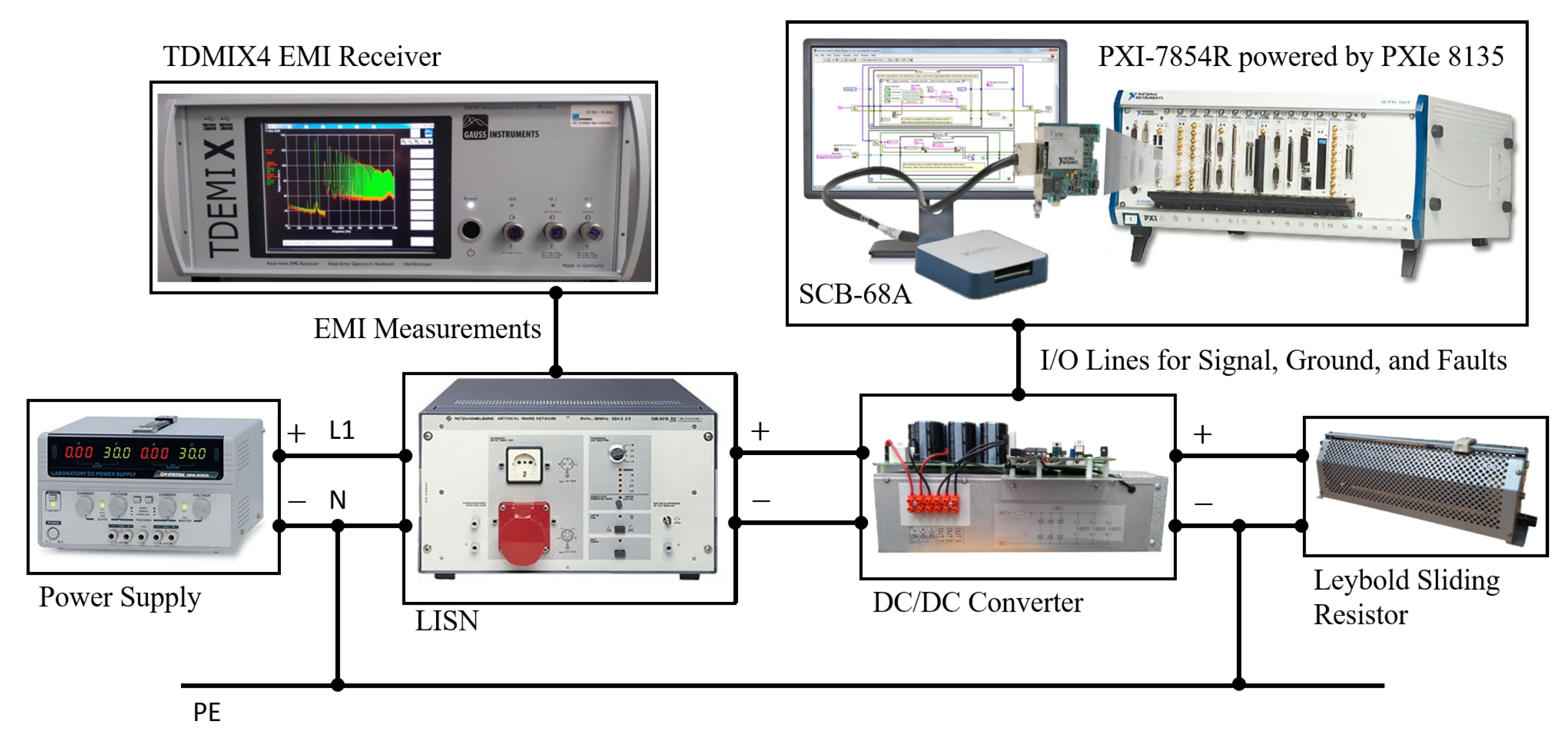
2. FPGA-Based Systems Design

2.1. FPGA Hardware

In the manuscript, we consider National Instruments PXIe-8135 controller as the primary development environment. The PXIe-8135 is an Intel Core i7 embedded controller with the design tool—LabVIEW. The development environment also includes the FPGA R-Series Multifunction RIO - PXI-7854R card (illustration in Figure 1) with VIRTEX-5 LX110 [11].
The PXI-7854R FPGA-based card has a few dozen Input/Output (I/O) resources, which include analog/digital converters (ADCs), digital/analog converters (DACs) and digital I/O lines. The design tool LabVIEW accesses the FPGA PXI-7854R device through the bus interfaces (PXI Triggers and PXI BUS). This connection makes possible timing, triggering, processing and custom I/O measurements, based on FPGA target programming, and most of it is available for demanded functions. Those required functions may use varied amounts of logic, besides using I/O resources. We assume that all control techniques require the same I/O resources, such as signals controlling transistors, or input faults. Therefore, the number of FPGA resources, used for logical and arithmetic operations, indicates the algorithmic complexity and it will be considered as one essential parameter to evaluate the control techniques implemented in FPGA.

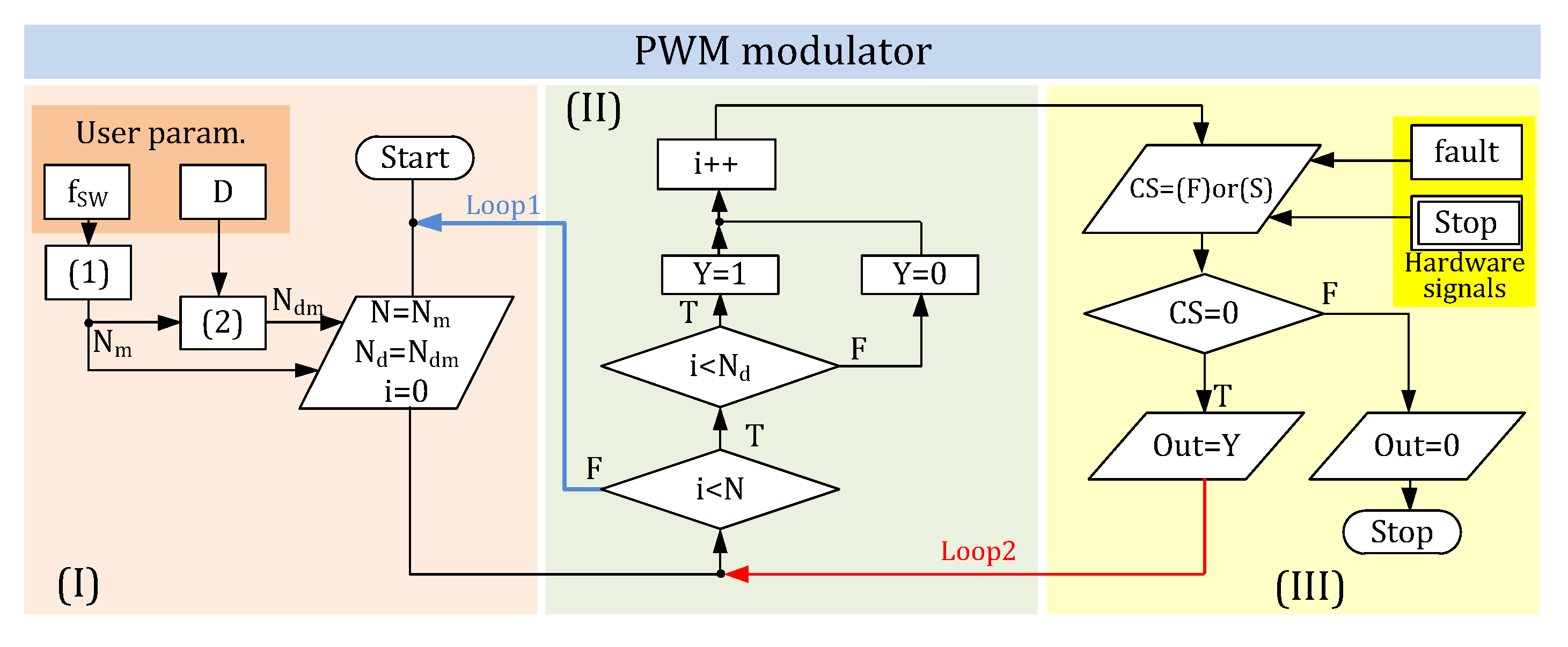
2.2. PWM Modulator Algorithm

To control the converter switches the PWM modulator is used. Figure 2 shows the main flowchart of the PWM modulator. For better visualization, we divide all operations into three (III) parts. In part I, the user may set the main control parameters: the average switching frequency f s w and duty cycle of the PWM signal D. Then, the program calculates the required number of clock ticks for the period (N) and the duration of high state ( N d ) according to the Equations (1) and (2).
N = f F P G A / ( f s w · S C T L )
N d = D · N
where: f F P G A —onboard available clock frequency, f s w —switching frequency and S C T L —single cycle timed loop (in clock ticks).
The index m (in Figure 2) means that the N d m and N m value is taken and recalculated for the m’th PWM period. The presented modulator can, therefore, cooperate with an external voltage controller and dynamically change the factor D. The duration of the period, represented by N m , may be constant for deterministic modulation (DetM) or may be changed randomly for RanM case. Part II illustrated the carrier function counter ramp represented by the variable i. Parameters N and N d are compared with the variable i to determine the value of output signal Y and control the loop I execution. Part III presents the generation of control (output) signal and the interaction with a C S function. In the presence of hardware signals of fault (F) or the stop button (S), the function C S returns 1, and the PWM operation is interrupted. The fault signal is typically generated by converter hardware in any emergency, while the stop signal is from the user. Figure 3 shows the operation of the modulator.

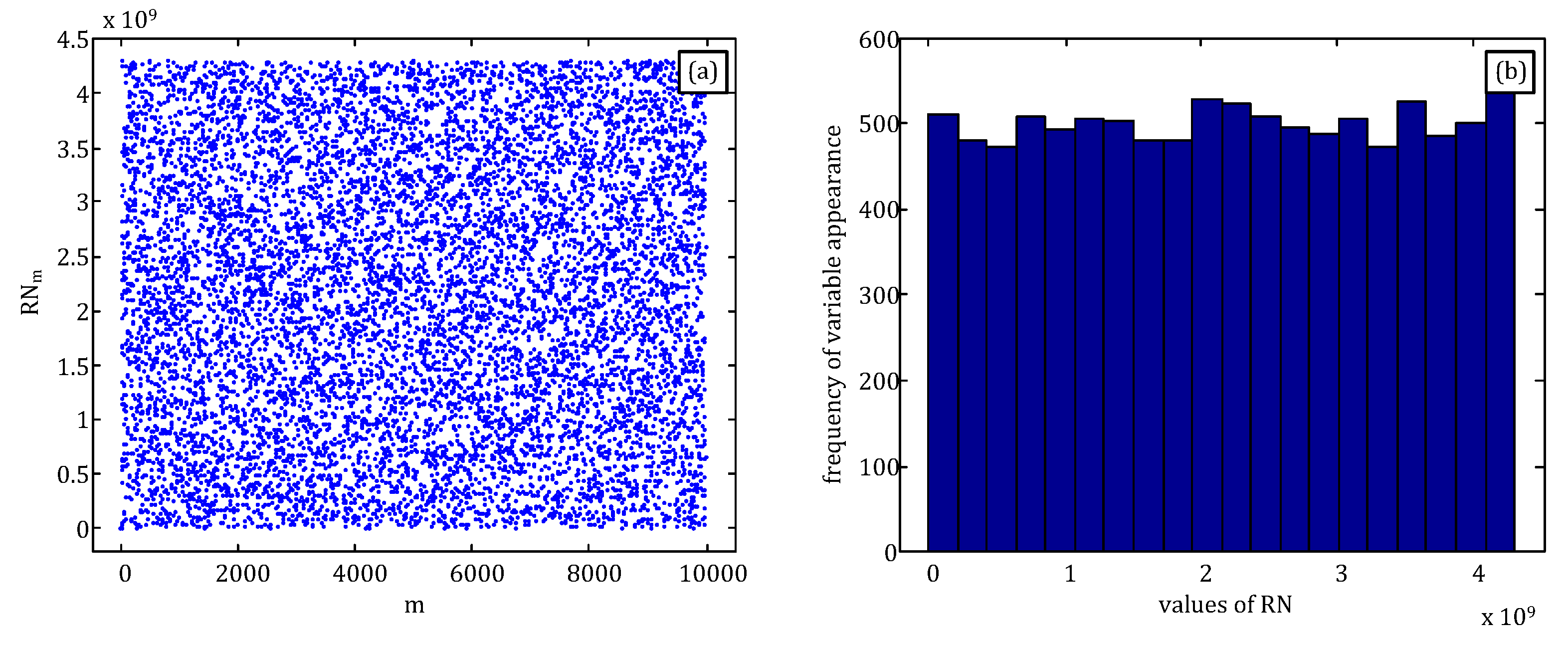
2.3. Random Number Generator

The main advantage of RanM instead DetM is highlighted in the literature [8,10,12,13,14,15] as the EMI noise reduction related to the f s w and its harmonics. The random number generator is crucial to the operation of RanM control algorithms. Since we consider FPGA features connected with the fixed-point operation, we propose to generate the random stream by a linear congruential generator (LCG). The LCG is a modular arithmetic algorithm, which provides a stream of pseudo-randomized numbers calculated with a Equation (3).
R N m = ( α · R N m 1 + c ) m o d n
where: R N m —the m’th random number provided by LCG, α , c , n —LCG coefficients.
The values of coefficients configured for the FPGA implementation were α = 17 and R N 0 = 17 , c = 0 and n = 2 32 . The modulo operation is made automatically due to the use of long integer variables with 32 bits of storage. For RanM, the generation of a random stream is done in a loop to get a new pseudo-random number for each PWM signal period. The presented LCG generates pseudo-random numbers with a period of 2 31 and a normal distribution. To show the property of a random stream, Figure 4 shows the 10,000 numbers R N m generated by LCG and their histogram/distribution.

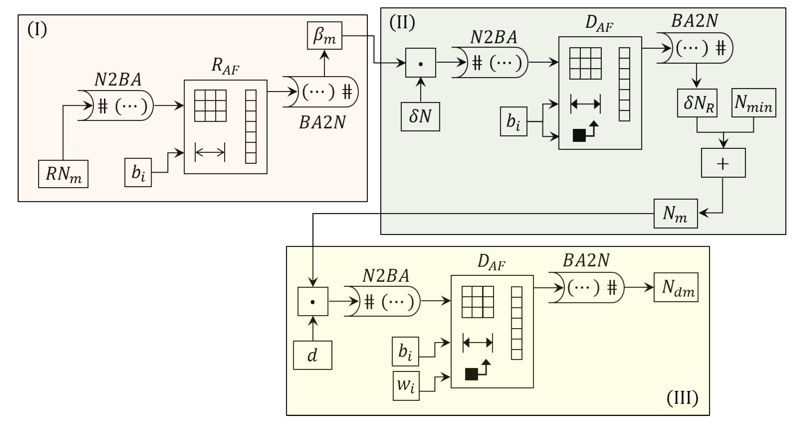
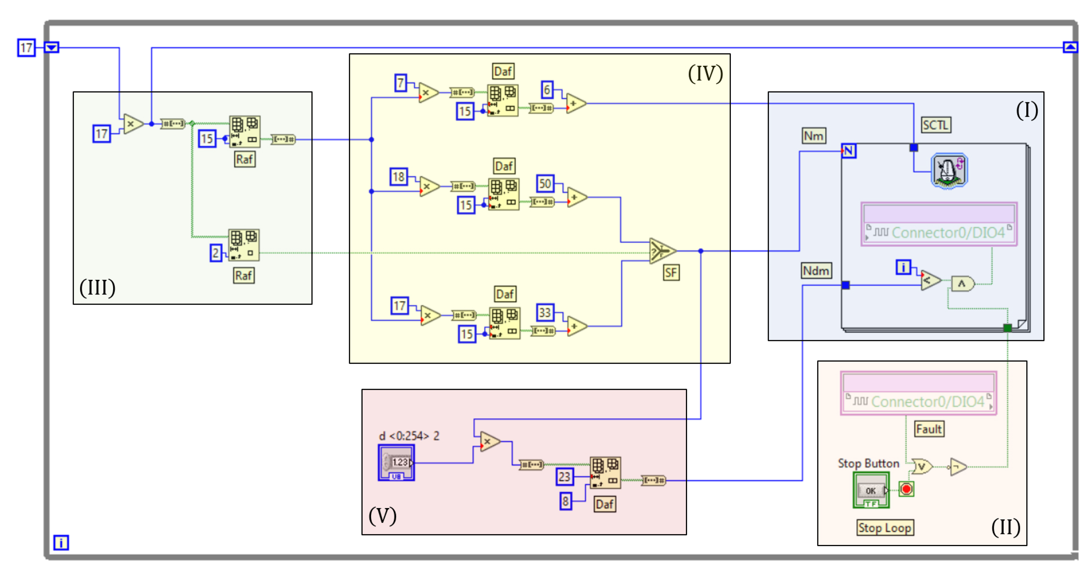
2.4. FPGA Implementation

This section presents the practical implementation of DetM and RandM in FPGA systems utilizing LabVIEW software. Additionaly, for RanM probability density function PDF analysis in MATLAB software will be shown.
Traditionally, during LabVIEW programming, we use modules with palettes of structures and functions. The number of such functions in LabVIEW FPGA Module is much smaller than for typical control devices with a microprocessor. Further, available functions can only operate on integer variables. Despite these drawbacks, the LabVIEW program Implementation in FPGA systems allows full control of program execution and high speed calculation. For instance, the LabVIEW FPGA Module has access to Single-Cycle Timed Loops (SCTL). The SCTL is a unique loop structure that executes all functions inside within one fixed time period ( S C T L ) [11]. The S C T L may be defined by the user as a time period or in ticks of the FPGA clock. In the control board used, the maximum clock frequency is 40MHz.
To realize the algorithm from Figure 2 in LabVIEW for FPGA, the While Loop structure with a sub-system For Loop was chosen. The For Loop corresponds to the loop II in Figure 2 and is executed N times. The While Loop corresponds to the loop I in Figure 2. The While Loop is performed until the C S function is activated. For DetM we consider the S C T L = 1 tick, and the number N = N m is constant.

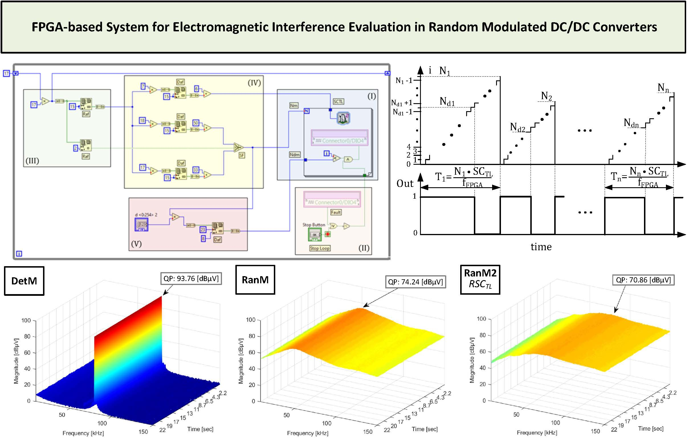
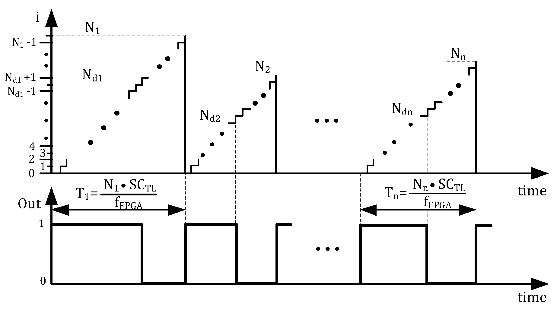
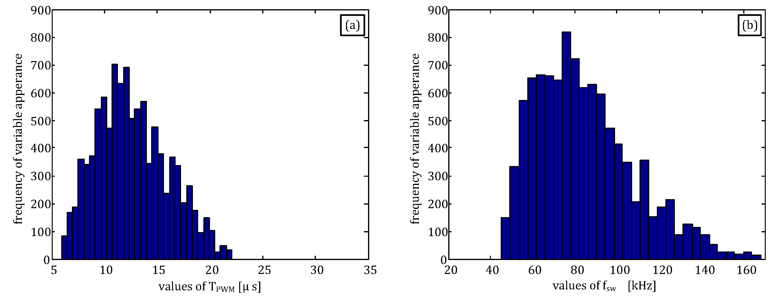
2.4.1. Single Randomization

For RandM the number N m is randomly changed for each PWM period using a random stream from the LCG (described in previous section). However, due to the use of fixed-point operations in FPGA, the resulting random number must be scaled (reduction of bit precision) to make it suitable for N m calculation. Figure 5 illustrates in the part I how to scale the R N m using the Reshaped Array Function ( R A F ) which is available in the LabVIEW environment.
Figure 5 shows in part I the parameter b i , which is responsible for providing the length of the output array and must be numeric. Before resizing, the number R N m is converted to a Boolean Array by the N 2 B A function. After resizing, the Boolean Array is converted to a number again by the B A 2 N function. As a result, a random number, β m , from 0 to 2 b i 1 is obtained. The next task is to calculate N m and N d m (from Figure 2), to change randomly according to the random β m number for each PWM period. The changes of the N m and N d m should also take place within the assumed range from the N maximum and minimum values. These operations should be performed with the appropriate precision in fixed-point arithmetic. However, LabVIEW software for FPGA does not allow direct actions of the mathematical division. The solution to the stated problem for N m calculation is shown in part II of the Figure 5. The δ N describes the maximum assumed changes in the PWM period and may be calculated as:
δ N = N m a x N m i n + 1 .
The δ N can be also represented relative to the average value of N, e.g., δ N = 50 % · N A V + 1 . Thus, for the first interaction illustrated in Figure 5, part II, consider the multiplication of the β m by δ N . Since a divide operation is not available, the Delete from Array Function ( D A F ) is applied to provide δ N R , a random stream that corresponds to the range between the 0 and the value of δ N 1 . In this step, the N m value is calculated using Equation (5). The final formula for calculating N m according to the concept from Figure 5, part II, is presented in Equation (6).
δ N R = ( ( ( R N m ( 32 b i ) ) · δ N ) b i )
N m = δ N R + N m i n
Although Equation (6) accurately describes random changes in the N value (which corresponds to the PWM period— T P W M ), it does not provide information on the average value. Therefore, later in the article, discussing RanM properties, we will give the average value of N N A V , and δ N , so the variation range of N is equal to N A V ± δ N / 2 . Choosing the right δ N is not apparent and should be the subject of a broader analysis. Despite, this topic will not be fully discussed in this article. However, we will show the basic challenges that face when choosing parameters for RanM.
We can take δ N value based on expected frequency randomization. For instance, if we assume that f s w = 80 kHz and this frequency may change ± 50 % , we will obtain m a x ( f s w ) = 80 kHz + 50% = 120 kHz, m i n ( f s w ) = 80 kHz − 50% = 40 kHz. The N m i n value will be related to 120 kHz and N m a x to 40 kHz (based on Equation (1)), so δ N = 1000 − 333 + 1 = 668. However, the value of N A V = 667 which does not correspond to a frequency of 80 kHz. Figure 6 shows the histogram of randomized N m values and the histogram of randomized frequencies f s w related to N m , for N A V = 667 with δ N = 668 . Figure 6b shows that switching frequency f s w varies within the assumed range from 40 to 120 kHz. Despite this, the frequency distribution is not uniform and the average frequency is not equal to 80 kHz. Adopting the δ N in such a way is therefore not particularly useful. Another possible approach to selecting δ N value may be made based on a relative change in time. Figure 7 shows the histogram of N m values and histogram of f s w , for N A V = 500 (value related to f s w = 80 kHz) with δ N = 334 so N < N A V ± 30 % > . In such a case, the average value of the frequency is closer to that intended, but the frequency distribution is still strongly non-linear.
Figure 5 shows in part III the D A F function with consideration of the set up of length and index of array, to provide calculation of N d m . We assumed that the coefficient d, represented as an 8 bit integer will be proportional to duty cycle factor D. The FPGA implementation considers the index value ( w i ) equal to 8, and the b i equal to 23. Thus, the final value of N d m is configurable, maintaining the proportionality with N m , within a range defined by d, as follows in Equation (7).
N d m = D · N m = ( ( d · N m ) > > w i ) = d · N m 2 w i
To calculate the period of PWM signal and its Duty cycle for RanM we use Equations (6) and (7), respectively. These equations are computed in the fixed time of a one loop execution— S C T L . We may consider the situation, in which the time S C T L is also changed randomly ( R S C T L ).

2.4.2. RanM with R S C T L —Additional Randomization

When we randomly change both the number of periods of the For Loop ( N m ) and the duration of this loop, we can talk about an additional randomization (RanM with R S C T L ). Basically, for R S C T L generation, we assume the same principle, as illustrated in Figure 5, part I and part II, however instead of S C T L = 1 tick we generate random value from 7 to 13. The m’th PWM period T P W M m is equal to ( N m · S C T L m ) / f F P G A . Figure 8 shows the histogram of the T P W M m and histogram of related f s w , for N = 50 , δ N = 34 and R S C T L < 7 : 13 > . Figure 8 shows that when we consider N m and R S C T L , the density distribution in both cases, (a) and (b), is changed. This approach of N m and R S C T L randomization gives us the possibility of shaping the density distribution. The frequency distribution is closer to the Gaussian distribution, which should be more favourable in terms of the average frequency and converter losses.

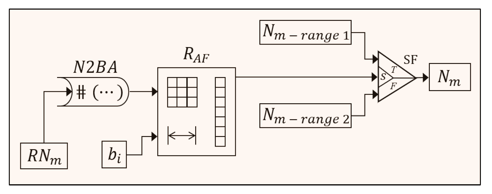
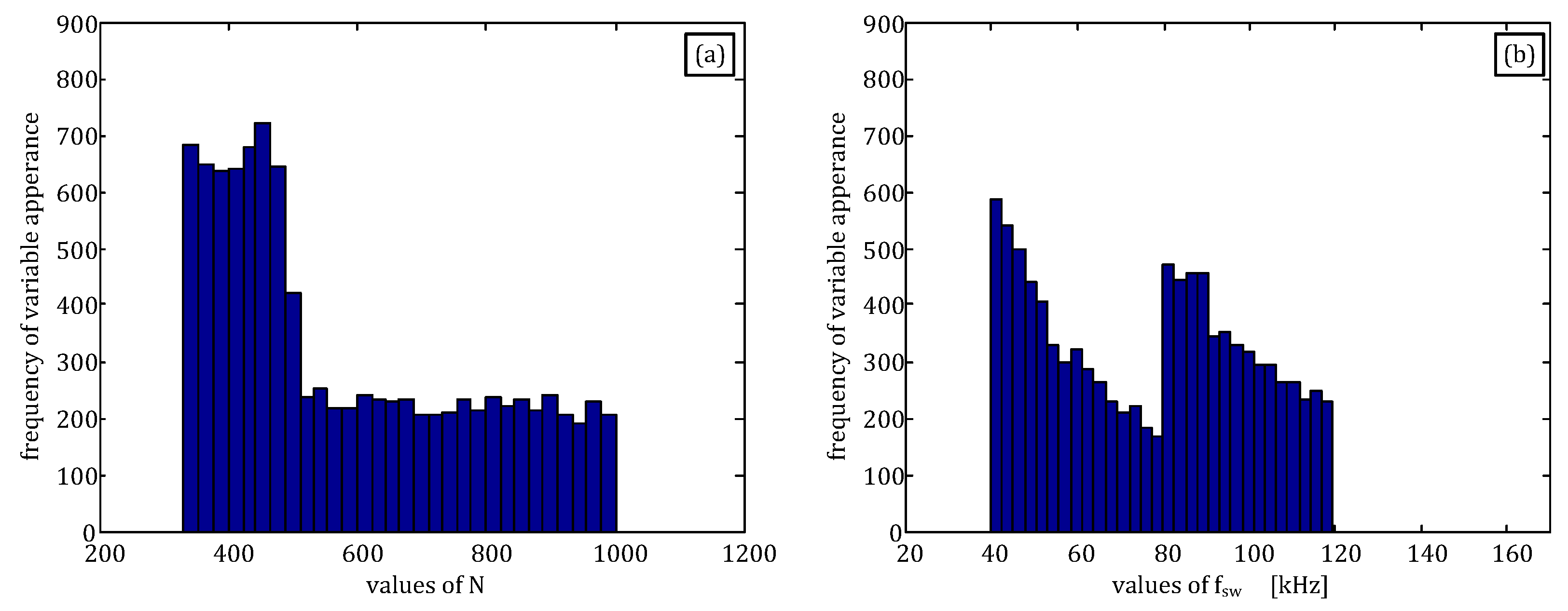
2.4.3. RanM2—Split Distribution of Variable
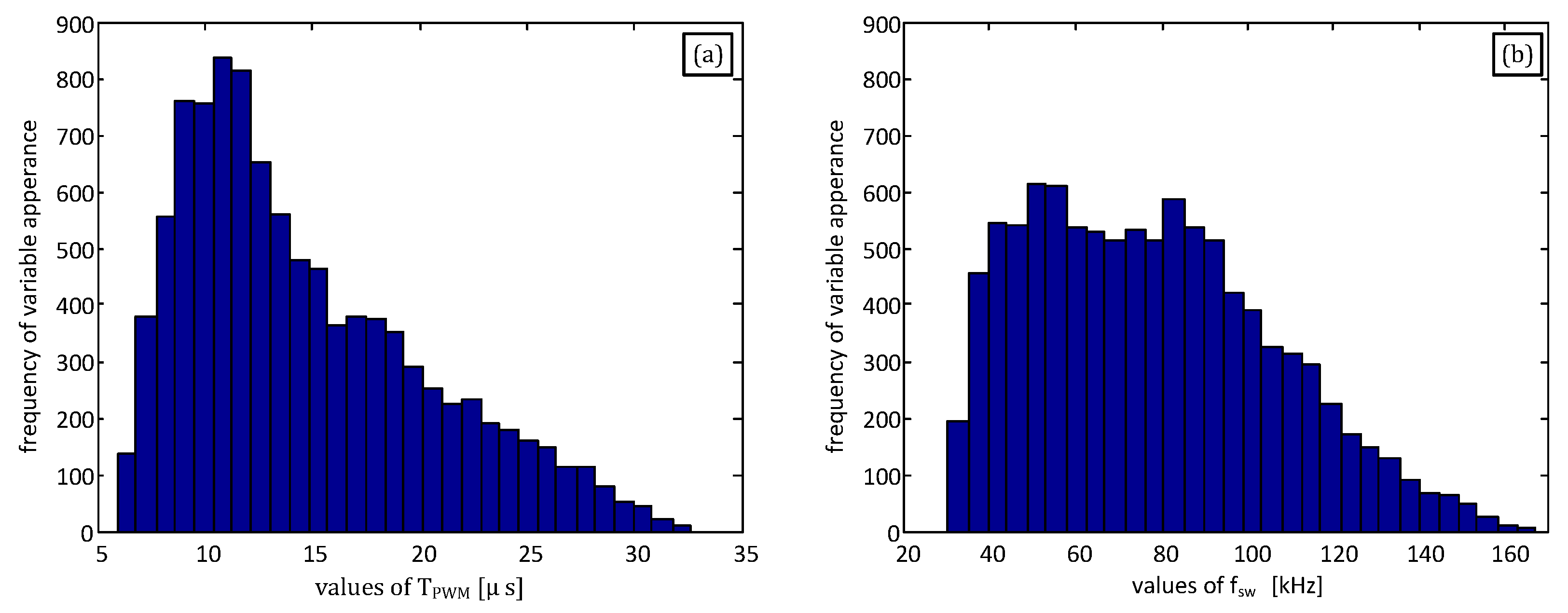
The other method to shape the T P W M m and f s w distributions is to split the N m distribution to a few sub-ranges in the entire N m range. For the presented FPGA implementation, we propose to use two predefined random sequence ranges. Then we consider the use of one random bit, digital 1 and 0 levels to choose the range of N m . The FPGA implementation is executed with a particular function ( S F ), which is available in the LabVIEW environment. The parameter S determines whether the S F returns the value wired to T or F. Thus, for each parameter, F or T, we assign one of the two predefined random sequence ranges, both provided by N m . Figure 9 illustrating the proposed FPGA implementation. We will denote random modulation with such a distribution as RanM2.
Figure 10 shows the histograms of N m values and their corresponding f s w values, for N A V 1 = 750 with δ N 1 = 500 and N A V 2 = 416 with δ N 2 = 167 .
As one can see, the use of two probability distributions for a PWM period (which is proportional to N m ) produces a more equal alignment of the frequency distribution. Therefore, in such a manner there is a possibility to create, with obvious limitations, the distribution of frequency.

2.4.4. RanM2 with R S C T L

The presented concept of two distributions of N m (RanM2) may be linked with the concept of additional randomization R S C T L . Figure 11 considers such a case with R S C T L < 7 : 13 > and for N A V 1 = 75 with δ N 1 = 50 and N A V 2 = 42 with δ N 2 = 17 . The obtained histograms are more smooth than histograms in Figure 10, which can be an advantage. However, the use of R S C T L increases the frequency spread.
Figure 12 shows the LabVIEW general program implemented in FPGA. In Figure 12, the parts corresponding to (I) and (II) refer to the basic modulator configuration (Figure 2). Therefore, it is applicable to both DetM and RanM. Part (III) presents the random number generator with a number scaling block, corresponding to part I of (Figure 5) and is used only for RanM, for both approaches of randomization discussed in Section 2.4 Parts (IV) and (V) correspond to part II and part III of (Figure 5), respectively. Since the FPGA needs to execute predefined random sequence ranges (the concept of additional randomization), the D A F function proportionally increases.

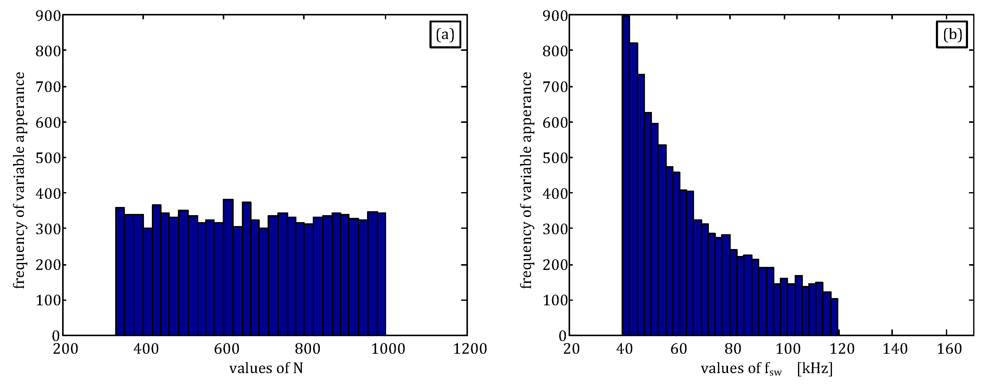
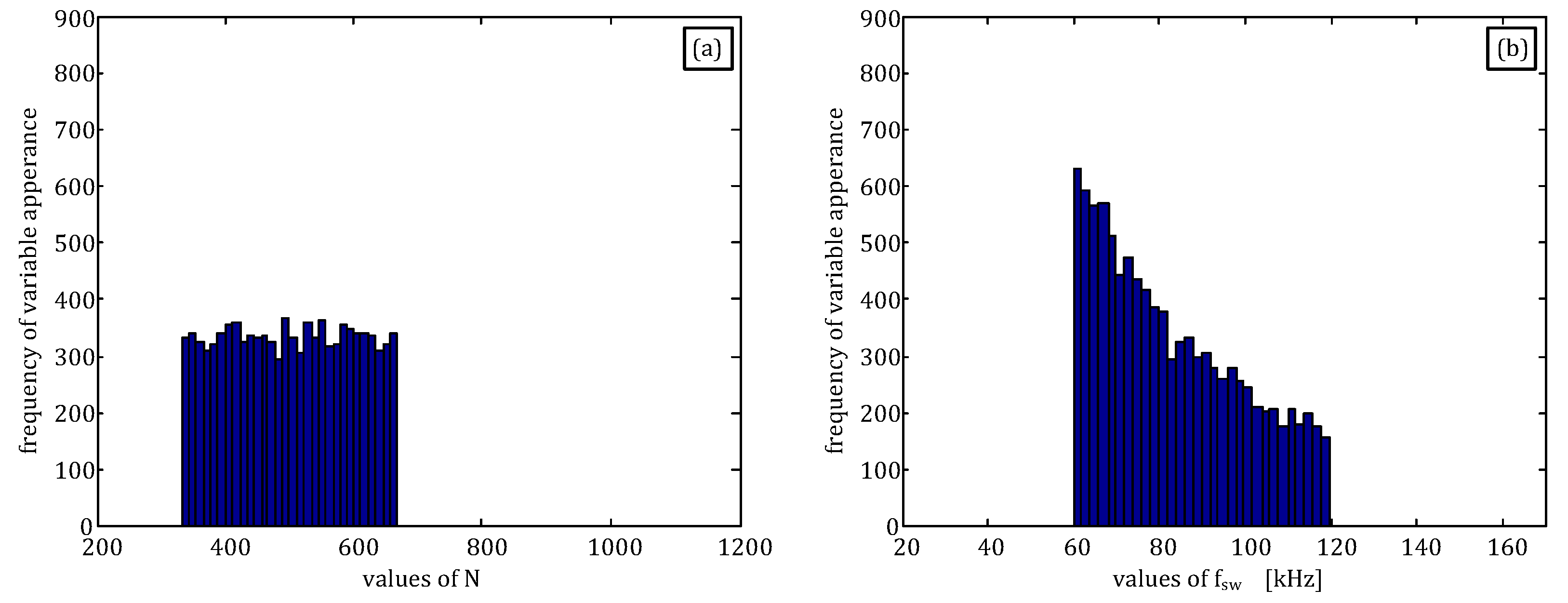
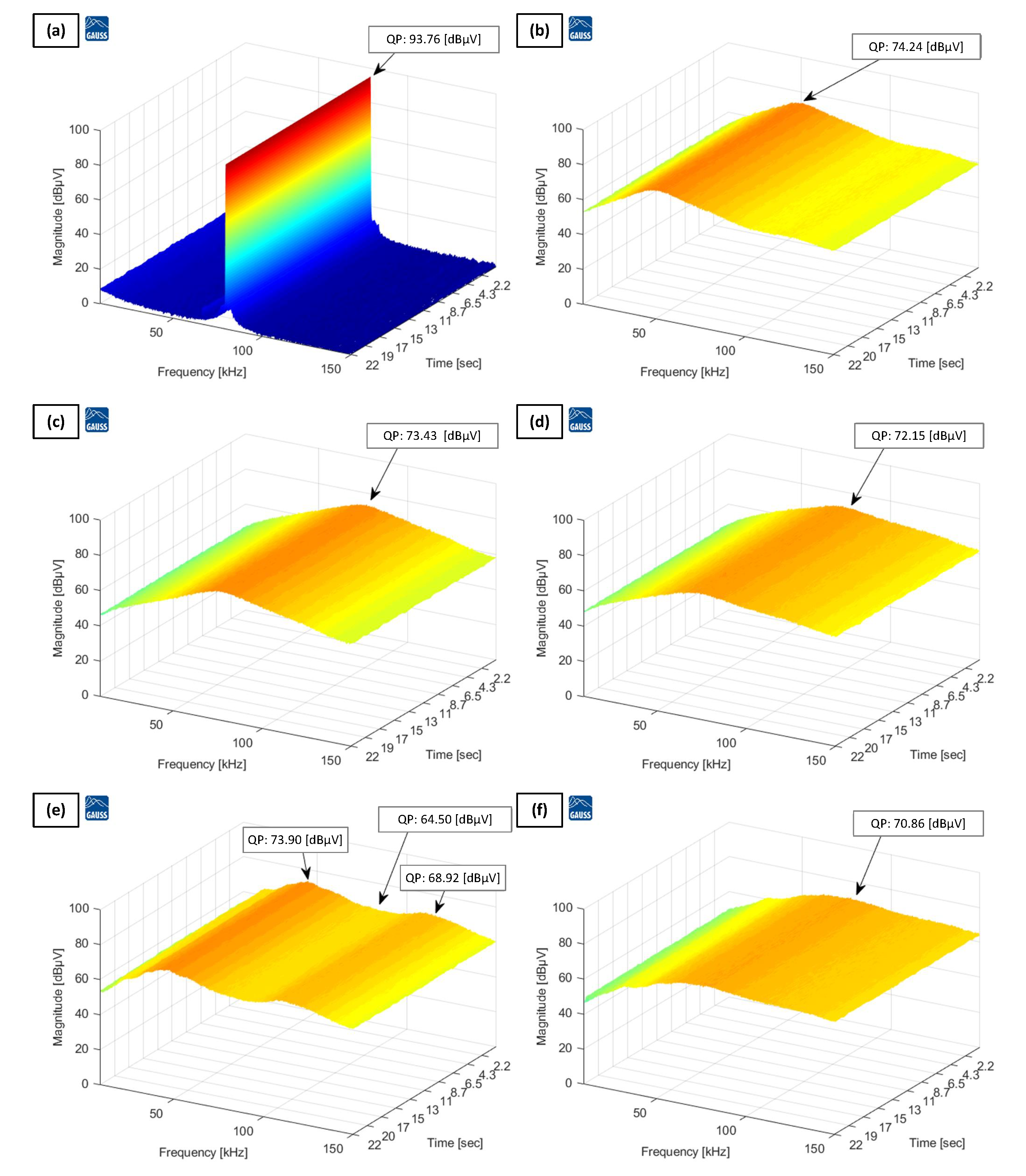
3. Experimental Results

This section provides the results of an experimental system. All presented analyses and measurements concern a buck-converter topology, with a C2-class high speed insulated-gate bipolar transistor (IGBT), and a hardware interface for signal and ground to the R-Series Multifunction RIO (FPGA PXI-7854R). The control signal output (RanM or DetM) is provided, at the hardware level, by the NI SCB-68A shielded connector block. Combined with the shielded cables, the SCB-68A provides rugged, very low-noise signal termination to the transistor gate drive. Figure 13 illustrates the scheme of the measuring testbed.
According to the schematic diagram illustrated in Figure 13, the buck-converter topology is powered by a regulated laboratory power supply. Additionally, the FPGA control board power is controlled by the PXIe 8135 to prevent additional couplings through the power source. A Leybold sliding resistor 320 Ω, 1.5 A was connected as load for the buck converter output. The EMI measurement was performed with the 50 Ω/50 μH Line Impedance Stabilization Network (LISN). The important parameters of the buck-converter and the testbed are summarized in Table 1.
Figure 14 shows the measurements for all cases (DetM and RanM) presented in Section 2. The results have been obtained using the TDMI X6 EMI receiver, which provides a 3D spectrogram for Quasi Peak (QP) detector, which is required by EMC standards in CISPR A frequency band.
The Figure 14a refers to the measurement for DetM with N m = N A V = 500 and δ N = 0 . The first harmonic magnitude (occurring at 80 kHz) is the most significant in the whole frequency spectrum. The magnitude of this harmonic is equal to 93.76 dBμV. The Figure 14b refers to measurement for RanM with N A V = 667 , δ N = 668 and S C T L = 1. As expected, the maximal harmonic magnitude is not connected with the f s w = 80 kHz. Despite this, the frequency varied within the assumed range (Figure 5), and the spectrum level is lowered to value 74.24 dBμV. The Figure 14c presents the measurement results for RanM with N A V = 500 , δ N = 330 and S C T L = 1. As expected, the maximal harmonic magnitude is lowered and its frequency is more connected with the f s w = 80 kHz. The maximum amplitude of the disturbances is equal in this case to 73.43 dBμV, and despite the smaller range of f s w , variation is lower than in the case of RanM from Figure 14b. Therefore, we can conclude that increasing the δ N range does not always lead to a lowering of the spectrum level. The Figure 14d refers to the measurement for RanM with N A V = 50 , δ N = 34 and R S C T L < 7 : 13 > . The maximal harmonic magnitude is connected with the f s w = 80 kHz, and a little EMI noise reduction is provided, whether compared with Figure 14b,c. The Figure 14e refers to the measurement for RanM2 for parameters: N A V 1 = 750 with δ N 1 = 500, N A V 2 = 416 with δ N 2 = 167, and S C T L . As expected, two extremes are visible in the spectrum. The Figure 14f shows the result of measurement for RanM2 with R S C T L (concept of additional randomization). The parameters of modulator are: R S C T L < 7 : 13 > , N A V 1 = 75 , δ N 1 = 50 , N A V 2 = 42 and δ N 2 = 17 . The EMI noise is spread with a better shape between all RanM proposed. Unfortunately, the spread of f s w value is the largest of the analysed cases (Figure 11). Based on the measurement, it is difficult in this case to determine the main/dominant frequency of disturbances.

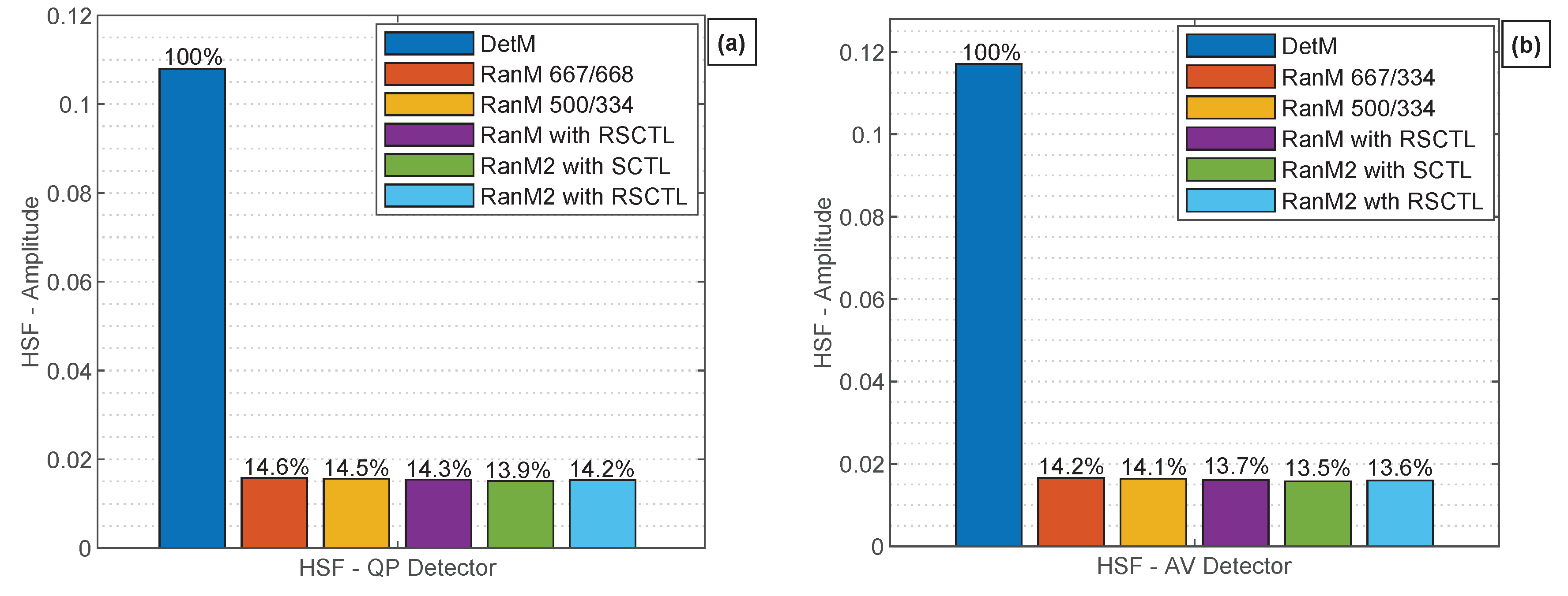
4. Discussion and Analysis of Results

According to Figure 14a, the maximum harmonic magnitude in the spectrum (observed at 80 kHz) for DetM is about 93.76 dBμV. Furthermore, Figure 14d shows the maximum harmonic magnitude in the spectrum (observed at 80 kHz) for RanM with R S C T L , which is about 72.15 dBμV. Therefore, RanM with R S C T L provides 21.61 dBμV for QP detector, with lower EMI levels than DetM. Applying the concept of additional randomization with R S C T L and sectional distribution of N m , RanM2 obtained the best results—Figure 14f. The results are about 22.90 dBμV for the QP detector, being lower than DetM. According to the literature, the evaluated harmonic reduction could also be provided by the Harmonic Spread Factor (HSF) [16,17]. The HSF is an accurate evaluation index of any waveform for testing its harmonic spreading effects, and is defined as follows in Equations (8) and (9).
H S F = 1 N j = 1 N ( H j H o ) 2
H o = 1 N j = 1 N ( H j )
where: H j is the amplitude of the jth harmonics and H o is the average value of all N harmonics.
The ideally spread spectrum must be near zero, i.e., white noise, presenting an HSF equal to zero. In this manuscript, the HSF analysis provides in absolute value, the harmonic reduction into CISPR A frequency band, for QP detector measurement and additionally for AV detector. Figure 15 shows the results of HSF calculation.
It is possible to observe that there are almost no differences between all HSF provided by RanM and RanM2 (for both QP and AV detectors). Of course, there is a significant difference between RanM2 and DetM. RanM2 based on the concept of additional randomization with S C T L presents the best HSF. However, whether compared with RanM2 based on the concept of additional randomization with R S C T L the difference is only 0.3% for QP and 0.1% for AV. In terms of EMI noise reduction, the difference between RanM2 with S C T L and with R S C T L is not too big for both detectors (less than 4 dB). Despite this, the frequency distribution was different in each case.
Additionally, hardware resources were also analysed. The hardware resources on an FPGA are indicated by the number of slices. The DetM code after the compilation process presents total slices of 3.0% from all available slices in the VIRTEX-5 LX110 FPGA. On the other hand, among all RM codes, the concept of additional randomization, RanM2 with R S C T L presents greater use of the number of slices, with 5.5%.

5. Conclusions

This manuscript demonstrates how to design RanM, and DetM oriented for FPGA implementation with the LabVIEW engineering software. Since there are some FPGA software limitations (fixed-point operation, and a lack of basic arithmetic functions), it may be challenging to complete the RanM and the DetM implementation. Therefore in the article, we have highlighted how to do some calculations required for PWM modulator implementation in FPGA. We have also shown that the realization of RanM in FPGA should consider the distribution of randomized time and frequency parameters of the PWM signal. One should pay the primary attention to the range of switching frequency f s w changes and the average value of this frequency.
The presented algorithms have been implemented in FPGA - R-Series Multifunction RIO (PXI-7854R), with VIRTEX-5 LX110. The most extensive version of the algorithm (RanM2 with R S C T L ) used only 5.5% of FPGA resources. Presented algorithms are weary simple, and they can be easily expanded. Likewise, implementing the modulator to a control system inside the same FPGA is also possible. Therefore, the proposed solutions can be used in all DC/DC converters applications. However, one may obtain the most significant benefits in automotive and lighting applications where there are direct limits on interference emission in the CISPR A band, and proposed control methods help fulfill these requirements.
Proposed modulators were tested experimentally. All measurements were carried out according to EMC standards in the frequency domain for CISPR A frequency band. The EMI emission (for design RanM) was significantly reduced compared to the DetM. We have achieved a reduction of the maximum EMI level value by over 20 dB. One should also remember, according to [8], that although pseudo-random modulations reduce the maximum level of interference, they do not change its aggregate power. Considering experimental research and implementation in FPGA, we assess that offered solutions have reached level 7 of Technology readiness levels (TRLs).
The differences between the EMI emission for different RanM were not significant. However, presented modulators differed in f s w distribution. The minimum value of f s w affects the operating conditions of the filters and and maximum amplitude of output current ripple. The maximum value of f s w frequency will be significant with the restrictions of the transistors. Keeping the average value of this frequency unchanged, we will not change the overall losses, and converter efficiency will be consistent. Therefore, by using the proposed methods (with appropriate parameters), one can achieve energy neutrality for the converter. In the future research, we are planning to investigate which shape of the frequency distribution is preferred in respect of EMI level emissions and other operation of the converter.

Author Contributions

Conceptualization, H.L., P.L., R.S. D.N. and W.S.; methodology, H.L., P.L. and R.S.; validation, formal analysis, visualization H.L. and P.L.; software, investigation, H.L.; writing—original draft preparation, H.L., P.L. and W.S.; writing—review and editing, H.L., P.L. and R.S.; supervision, project administration, funding acquisition, R.S. All authors have read and agreed to the published version of the manuscript.

Funding

This paper is part of a project that has received funding from the European Union’s Horizon 2020 research and innovation program under the Marie Skłodowska-Curie grant agreement No 812391–SCENT.

Conflicts of Interest

The authors declare no conflict of interest.

Abbreviations

The following abbreviations are used in this manuscript:
AVAverage
DetMDeterministic Modulation
DSPDigital Signal Processors
EMCElectroMagnetic Compatibility
EMIElectroMagnetic Interference
FPGAFiled-Programmable Gate Array
HSFHarmonic Spread Factor
LGGLinear Congruential Generator
LISNLine Impedance Stabilization Network
PDFProbability Density Function
QPQuasi Peak
PWMPulse-Width Modulation
RanMPseudo-Random Modulator

References

  1. Estrela, V.V.; Saotome, O.; Loschi, H.J.; Hemanth, J.; Farfan, W.S.; Aroma, J.; Saravanan, C.; Grata, E.G. Emergency response cyber-physical framework for landslide avoidance with sustainable electronics. Technologies 2018, 6, 42. [Google Scholar] [CrossRef] [Green Version]
  2. Smoleński, R. Selected conducted electromagnetic interference issues in distributed power systems. Bull. Pol. Acad. Sci. Tech. Sci. 2009, 57, 383–393. [Google Scholar] [CrossRef]
  3. Peng, Q.; Jiang, Q.; Yang, Y.; Liu, T.; Wang, H.; Blaabjerg, F. On the Stability of Power Electronics-Dominated Systems: Challenges and Potential Solutions. IEEE Trans. Ind. Appl. 2019, 55, 7657–7670. [Google Scholar] [CrossRef]
  4. Yuan, B.; Liu, M.X.; Ng, W.T.; Lai, X.Q. Hybrid Buck Converter With Constant Mode Changing Point and Smooth Mode Transition for High-Frequency Applications. IEEE Trans. Ind. Electron. 2019, 67, 1466–1474. [Google Scholar] [CrossRef]
  5. Arunkumari, T.; Indragandhi, V. An overview of high voltage conversion ratio DC-DC converter configurations used in DC micro-grid architectures. Renew. Sustain. Energy Rev. 2017, 77, 670–687. [Google Scholar] [CrossRef]
  6. Loschi, H.; Ferreira, L.; Nascimento, D.; Cardoso, P.; Carvalho, S.; Conte, F. EMC Evaluation of Off-Grid and Grid-Tied Photovoltaic Systems for the Brazilian Scenario. J. Clean Energy Technol. 2018, 6, 125–133. [Google Scholar] [CrossRef] [Green Version]
  7. Bojarski, J.; Smolenski, R.; Lezynski, P.; Sadowski, Z. Diophantine equation based model of data transmission errors caused by interference generated by DC-DC converters with deterministic modulation. Bull. Pol. Acad. Sci. Tech. Sci. 2016, 64, 575–580. [Google Scholar] [CrossRef]
  8. Lezynski, P. Random modulation in inverters with respect to electromagnetic compatibility and power quality. IEEE J. Emerg. Sel. Top. Power Electron. 2017, 6, 782–790. [Google Scholar] [CrossRef]
  9. Kubík, Z.; Skála, J. Electromagnetic Interference from DC/DC Converter of Photovoltaic System. In Proceedings of the International Conference on Applied Electronics (AE), Pilsen, Czech Republic, 15 April 2019; pp. 1–4. [Google Scholar]
  10. Lezynski, P.; Smolenski, R.; Loschi, H.; Thomas, D.; Moonen, N. A novel method for EMI evaluation in random modulated power electronic converters. Measurement 2020, 151, 107098. [Google Scholar] [CrossRef]
  11. National Instruments Corporation, Multifunction RIO, NI R Series Multifunction RIO User Manual NI 781xR, NI 783xR, Ni 784xR, and NI 785xR Devices. Technical Report 370489G-01 . June 2009. Available online: https://www.ni.com/pdf/manuals/370489g.pdf (accessed on 8 May 2020).
  12. Lai, Y.S.; Chen, B.Y. New random PWM technique for a full-bridge DC/DC converter with harmonics intensity reduction and considering efficiency. IEEE Trans. Power Electron. 2013, 28, 5013–5023. [Google Scholar] [CrossRef]
  13. Chatterjee, S.; Garg, A.K.; Chatterjee, K.; Kumar, H. Chaotic PWM spread spectrum scheme for conducted noise mitigation in DC-DC converters. In Proceedings of the International Conference on Energy, Power and Environment: Towards Sustainable Growth, Shillong, India, 12 June 2015; pp. 1–6. [Google Scholar]
  14. Marsala, G.; Ragusa, A. Spread spectrum in random PWM DC-DC converters by PSO&GA optimized randomness levels. In Proceedings of the 5th International Symposium on Electromagnetic Compatibility (EMC-Beijing), Beijing, China, 28–31 October 2017; pp. 1–6. [Google Scholar]
  15. Gamoudi, R.; Chariag, D.E.; Sbita, L. A Review of Spread-Spectrum-Based PWM Techniques—A Novel Fast Digital Implementation. IEEE Trans. Power Electron. 2018, 33, 10292–10307. [Google Scholar] [CrossRef]
  16. Liou, W.R.; Villaruza, H.M.; Yeh, M.L.; Roblin, P. A digitally controlled low-EMI SPWM generation method for inverter applications. IEEE Trans. Ind. Inform. 2013, 10, 73–83. [Google Scholar] [CrossRef]
  17. Jing, H.; Weiying, Z.; Jinhong, L. Study on improving EMC of APFC converter with chaotic spread-spectrum technique. In Proceedings of the 2nd Advanced Information Technology, Electronic and Automation Control Conference, Chongqing, China, 25–26 March 2017; pp. 433–437. [Google Scholar]
Figure 1. Field-Programmable Gate Array (FPGA) PXI-7854R illustration [11].
Energies 13 02389 g001
Figure 2. The main flowchart of the PWM modulator, providing parameters (I), counter ramp (II), and generation of output signal (III).
Energies 13 02389 g002
Figure 3. The principle of the PWM operation.
Energies 13 02389 g003
Figure 4. R N m distribution (a), and histogram (b).
Energies 13 02389 g004
Figure 5. The scheme of the R N m scaling process, led to lower bit precision (I), and for calculating the random stream of N m (II) and N d m (III).
Energies 13 02389 g005
Figure 6. Histogram of N m ticks distribution (a), and histogram of frequency distribution (b), for N A V = 667 and δ N = 668 .
Energies 13 02389 g006
Figure 7. Histogram of N m ticks distribution (a) and histogram of frequency distribution (b), for N A V = 500 and δ N = 333 .
Energies 13 02389 g007
Figure 8. Histogram of T P W M m distribution (a) and histogram of related f s w distribution (b), for N A V = 50 with δ N = 34 , and R S C T L < 7 : 13 > .
Energies 13 02389 g008
Figure 9. Illustration of N m generation in proposed RanM2.
Energies 13 02389 g009
Figure 10. Histogram of N m ticks distribution (a) and histogram of frequency distribution (b), for RanM2 with parameters: N A V 1 = 750 with δ N 1 = 500 and N A V 2 = 416 with δ N 2 = 167 .
Energies 13 02389 g010
Figure 11. Histogram of N m ticks distribution (a) and frequency distribution (b), for RanM2 with R S C T L with parameters: R S C T L < 7 : 13 > , N A V 1 = 75 , δ N 1 = 50 , N A V 2 = 42 and δ N 2 = 17 .
Energies 13 02389 g011
Figure 12. LabVIEW general program implemented in FPGA, for loop (counter ramp) and output signal generation (I), conditions for stopping the program II), random number generator (III), N m and S C T L calculation (IV), and N d m calculation (V).
Energies 13 02389 g012
Figure 13. Schematic diagram of measuring testbed.
Energies 13 02389 g013
Figure 14. The electromagnetic interference (EMI) spectrum for DetM with N = 500 (a), RanM with N A V = 667 , δ N = 668 (b), RanM with N A V = 500 , δ N = 330 (c), RanM with R S C T L for N A V = 50 , δ N = 34 and R S C T L < 7 : 13 > (d), RanM2 with N A V 1 = 750 , δ N 1 = 500 , N A V 2 = 416 , δ N 2 = 167 (e), RanM2 R S C T L < 7 : 13 > , N A V 1 = 75 , δ N 1 = 50 , N A V 2 = 42 and δ N 2 = 17 (f).
Energies 13 02389 g014
Figure 15. Harmonic Spread Factor (HSF) calculations: (a) detector Quasi Peak (QP) and (b) detector Average (AV).
Energies 13 02389 g015
Table 1. The main parameters of buck-converter topology.
Component/FunctionSpecification
Transistors typeIXGH40N60C2D1
I C (max)40 A
t o n 40 ns
t o f f 180 ns
Transistor Gate DriversHCPL-316J
Converter Power1800 W (max)
DC capacitors1500 μF
Max DC voltage450 V
Loadsliding resistor 320 Ω (max), 1.5 A (max)

