Article

Novel Soft-Switching Integrated Boost DC-DC Converter for PV Power System

1
Faculty of Engineering, Sohag University, Sohag 82524, Egypt
2
Faculty of Engineering, Alasala Colleges, Dammam 31483, Saudi Arabia
3
Faculty of Engineering, Assiut University, Assiut 71518, Egypt
*
Author to whom correspondence should be addressed.
Energies 2020, 13(3), 749; https://doi.org/10.3390/en13030749
Submission received: 26 December 2019 / Revised: 22 January 2020 / Accepted: 3 February 2020 / Published: 8 February 2020
(This article belongs to the Section A2: Solar Energy and Photovoltaic Systems)

Abstract

:
This paper presents a novel soft-switching boost DC-DC converter, which uses an edge-resonant switch capacitor based on the pulse width modulation PWM technique. These converters have high gain voltage due to coupled inductors, which work as a transformer, while the boost converter works as a resonant inductor. Upon turning on, the studied soft switching circuit works at zero-current soft switching (ZCS), and upon turning off, it works at zero-voltage soft switching (ZVS) while using active semiconductor switches. High efficiency and low losses are obtained while using soft switching and auxiliary edge resonance to get a high step-up voltage ratio. A prototype model is implemented in the Power Electronics Laboratory, Assiut University, Egypt. Seventy-two-panel PV modules of 250 W each were used to simulate and execute the setup to examine the proposed boost converter.

1. Introduction

Recently, vigorous attempts have been made to attain optimized switch-mode power converter circuits with which to interface renewable energy sources to a utility such as a solar photovoltaic PV, fuel cell, and supercapacitor banks. To increase the dependence of the power electronics system and the power conversion capability, the expansion of boost DC-DC circuits is needed with modern control schemes [1,2,3,4,5]. Solar photovoltaics have been introduced as a future power source, due to the increasing need for clean energies and power-distributed generation systems. Injecting the generated energy into the network (grid) requires power conditioning circuits. In general, a higher step-up ratio DC-DC circuit is required for boosting the low PV voltage to a higher voltage output. Using conventional circuits such as cascade DC-DC power converters leads to additional cost and system complexity. Moreover, the conventional fly-back DC-DC converter topologies have leakage constituents that lead to voltage stresses on the semiconductor switches and more power losses, resulting in lower circuit efficiency.
To improve the energy conversion efficiency of the PV system in this paper, a soft-switched boost-type converter using an additional simple resonant cell is adopted. The auxiliary resonant circuit consists of a resonant inductor, an auxiliary switch, auxiliary diodes, and a resonant capacitor. As mentioned above, the traditional boost converter has decreased efficiency due to regularly being turned on and off, which generates switching losses. As we know, increasing the switching frequency will increase the periodic switching and conduction losses, resulting in an increase in the energy loss of the total system. To decrease these losses, we propose a soft-switching arrangement. This can be achieved by adding an auxiliary circuit, as shown in Figure 1a, instead of a classical hard-switched converter [6]. Moreover, the auxiliary circuit has no additional complexity or cost.
To reduce the weight and size, a higher switching frequency operation, i.e., in the range of more than 50 kHz, is utilized [7]. In traditional switching converters, the exemplary switching frequency is between 5 kHz and 20 kHz. The switching frequency generally cannot be increased because this results in increasing switching losses and stresses on semiconductor devices. A high frequency is utilized to reduce the volume and weight of passive devices. The dynamic performance is better in the case of higher frequencies. High-frequency switching speeds up the converter response time and reduces the output filter volume, cost, and size. A high switching frequency is desirable for the minimum output inductor size and maximum control loop bandwidth. Overall system size will be reduced due to the operation of switches at a high frequency, which will make the new converters more feasible. To overcome these problems, soft-switching schemes such as zero-voltage soft switching (ZVS) type or zero-current soft switching (ZCS) commutation should be utilized to reduce switching losses and the semiconductor device stresses. For power converters in a distributed PV system, a soft-switching technique is proposed [8,9,10,11,12]. The presented converter (see Figure 1b) has advantages of improved efficiency at a higher switching frequency, low leakage current, wide load range, reduced weight and size, and a maximum total efficiency of 97.1% at a switching frequency of 100 kHz.
The problems of excessive electromagnetic interference EMI and low efficiency can be solved by using zero-voltage-transition (ZVT) converters by limiting the turning-off di/dt in the output-side rectifier. Various types of ZVT converters have been presented before [9,13], but these converters suffer from several drawbacks, such as the following.
(1)
Most ZVT converter topologies have the auxiliary switch with hard-switching turned off, which, of course, limits the efficiency of such converters; see Figure 1c [13].
(2)
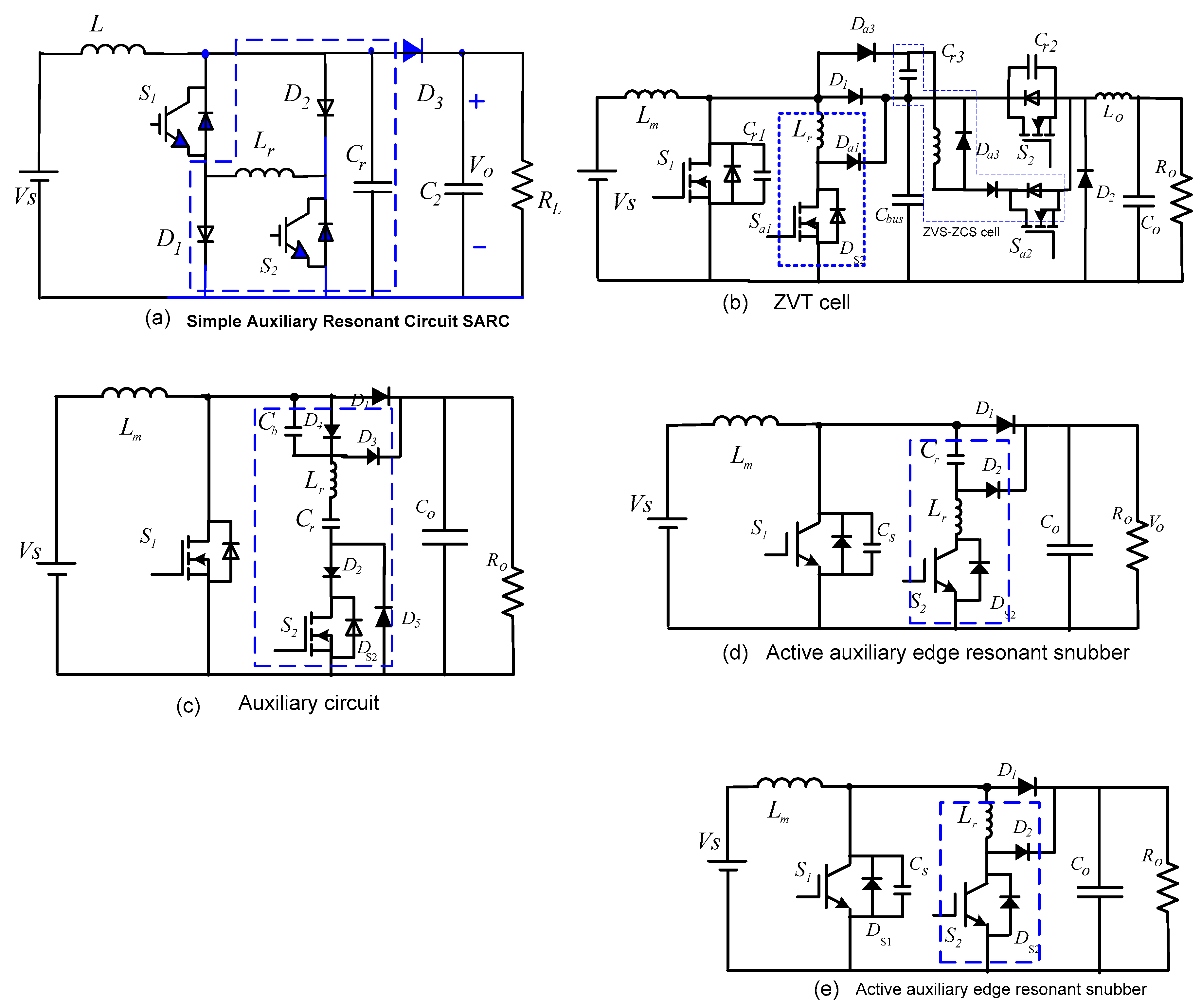
The auxiliary circuits increase the complexity of the system because they consist of several active and passive components. Moreover, the auxiliary semiconductor switches require a floating gate drive.
(3)
The elements of auxiliary circuits suffer from a higher voltage and current stresses.
(4)
The conduction losses are high in auxiliary circuit components [14].
Figure 1d shows the configuration circuit of boost type based on an edge-resonance ZVS-PWM DC-DC converter circuit utilizing IGBTs as active switches [15]. This converter is considered a conventional chopper-fed, boost-type power converter circuit. This converter also includes an auxiliary active resonance-snubber circuit, which includes a resonance capacitor Cr, a resonant inductor Lr, an auxiliary active power switch S2, a lossless snubber capacitor Cs, and diode D2 in the auxiliary circuit.
An improved circuit of a DC-DC power converter was proposed in [16]. The problem in this power electronics circuit, shown in Figure 1e, is that the auxiliary switch is turned-off under the hard-switching condition. However, the used auxiliary switch in the chopper-fed DC-DC circuit, shown in Figure 1e, can operate under the ZCS operation condition at turn-off transition by adding a simple resonance capacitor Cr.
Recent research has been based on the combination of a PV module with a power converter, which addresses all the required control requirements, such as the tracking of maximum and output voltage regulation. An inclusive literature review for nonisolated single-phase PWM inverters for a PV-integrated AC module is presented in [17,18].
In [19], parallel-connected converters for solar PV arrays are studied. Similar to the AC solar PV arrays applications, the output voltage of solar PV arrays is low, so a high-efficiency DC-DC converter is required. The high gain nonisolated DC-DC circuits which are used in the implementation of converter circuits are studied [20,21,22,23]. Previous works have used soft-switching coupled inductors [24,25,26,27,28,29,30,31,32,33,34,35,36].
A novel circuit for the boost DC-DC converter interfacing PV systems is introduced in this paper. In the following section, the paradigm design details of the suggested circuit are revealed. The behavior of the inverter system stage was similar to constant power load, not like resistive load, by placing a battery load at the output of the boost stage. The boost converter stage can be managed to draw a certain amount of current determined by the inductor rating and the duty cycle, depending on the loading conditions. The introduced converter is also studied in continuous and discontinuous modes of conduction. Also, the efficiency of the converting system is improved. The converting system consists of a solar PV array and a soft-switching boost DC-DC converter, which uses an auxiliary resonant circuit, auxiliary switch, diode, inductance, and capacitance. The traditional boost converters have lower efficiency due to hard switching, which increases losses due to on/off operations.
In Section 2, PSIM is presented, which is a well-known simulation program assisting in the modeling and simulation of the solar PV system and consists of a closed-loop control converter system. The strategy of control and steady-state analysis is discussed. Section 3 clarifies the operation principle via the operation interval waveforms and the relevant equivalent circuits. Section 4 presents the control scheme of the proposed power converter. The experimental results of the implemented boost converter are presented in Section 5. Using several power levels, output voltages and currents are studied and measured.

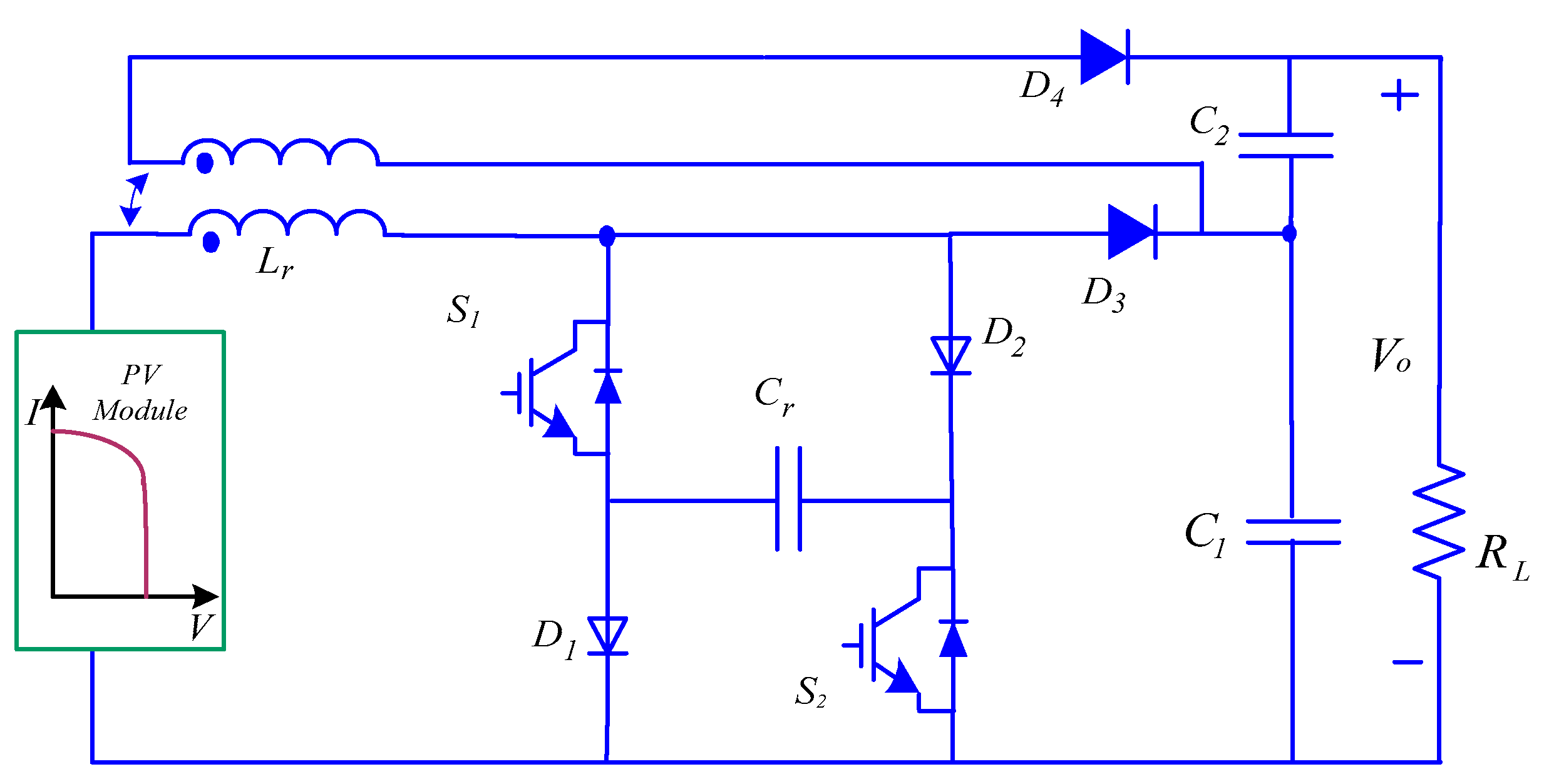
2. Design of the Circuit

The edge-resonance switched-capacitor (ER-SC) converter includes two active IGBT switches, i.e., S1, S2, connected to two auxiliary diodes D1, D2. The resonance is formed by a resonance capacitor Cr and a resonance coupled inductor Lr. The circuit configuration of the proposed soft-switching ER-SC boost DC-DC converter circuit is illustrated in Figure 2. A voltage doubler is composed of D4, C2, and coupled inductor Lr. The main advantages of the proposed soft-switching ER-SC boost PWM DC-DC converter are as follows.
(1)
Higher step-up voltage gain can be obtained due to the occurrence of edge resonance formed by elements Lr and Cr.
(2)
Power losses are reduced due to soft-switching operation; this improves efficiency.
(3)
ER-SC involves a module or modules as the basis of a configurable design by simple circuit construction and H-bridge IGBT module.
(4)
The current participation operation is obtainable between S1 and S2, which is efficient for the applications that have high current input.
(5)
The PWM gate signal for S1 and S2 can be general; thereafter, the gate driver circuits are simpler than that for the conventional converter.

3. Principle of Operation

During each commutation period of the boost converter operation, there are five operating intervals. The operating current waveforms are illustrated in Figure 3. Five switching intervals take place through one operating period. The subsequent equivalence circuits of operating intervals of the studied circuit during one switching period are shown in Figure 4. To analyze the proposed DC-DC converter circuit, the output current and voltage waveforms are shown in Figure 5. The theory of operation of the converter is demonstrated in the subsequent sections using the corresponding switching interval equipollent circuits.

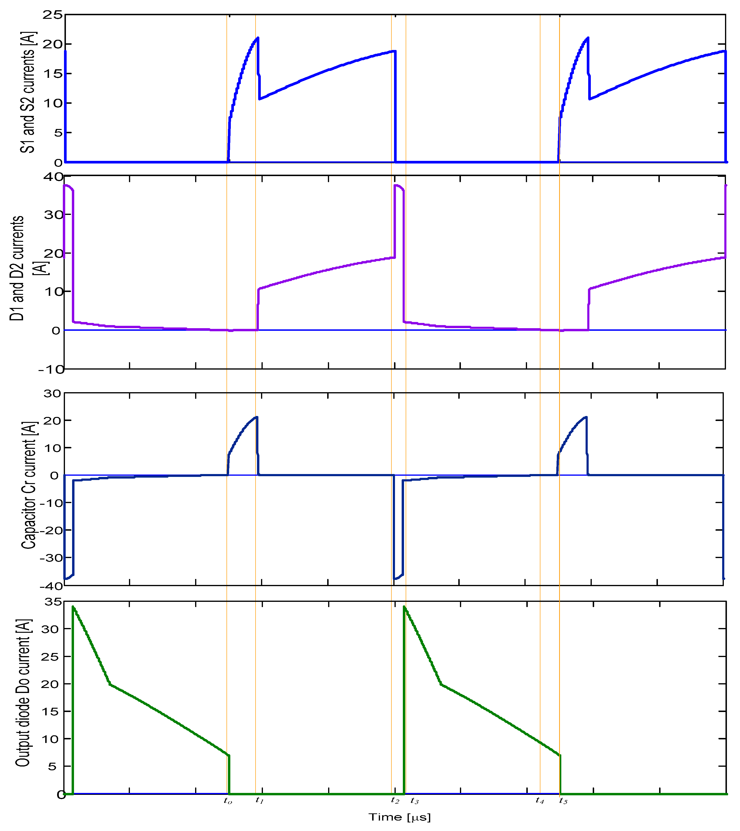
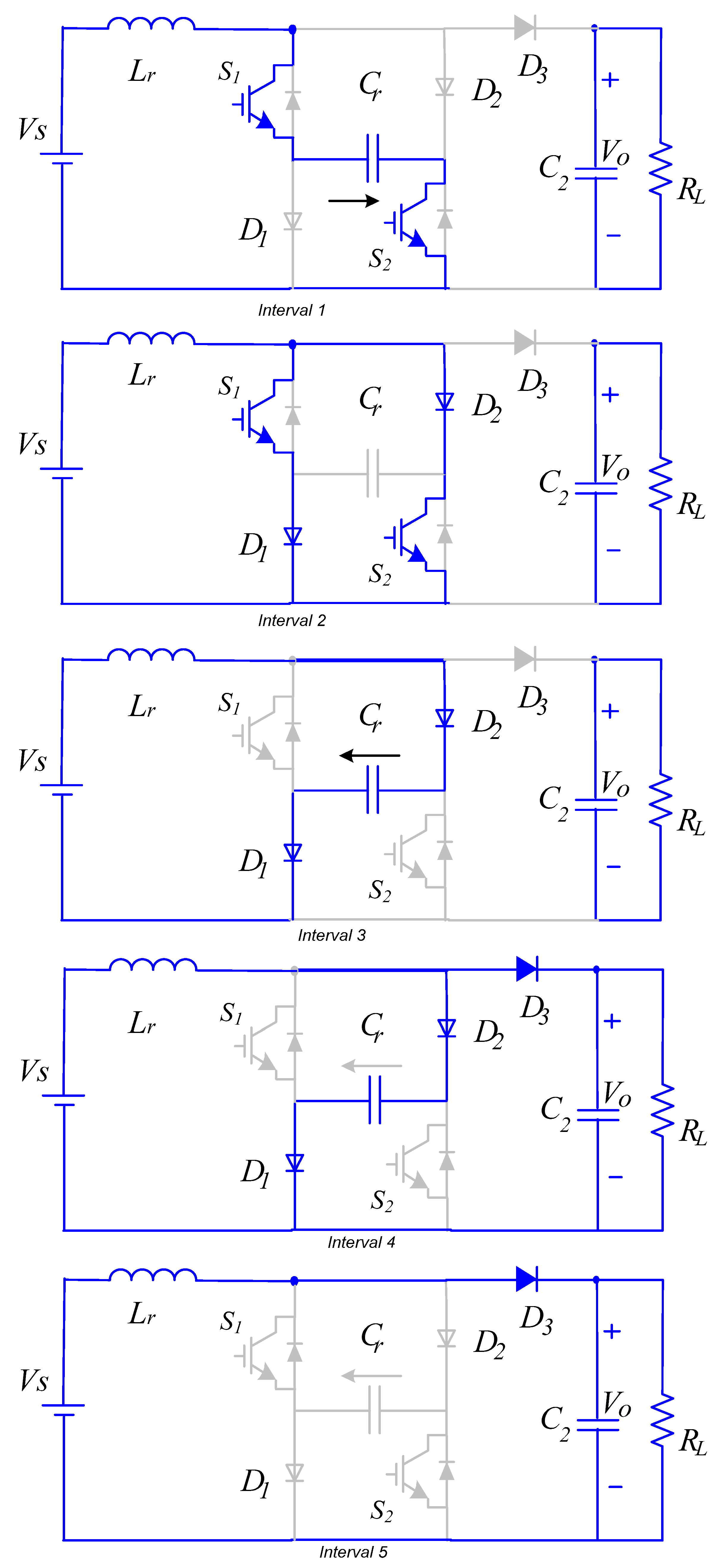
3.1. Interval 1: to ≤ t < t1 (S1 and S2: ON, D1, D2, and D3: OFF)

This mode is called the ZCS turn-on interval. The active power switches S1 and S2 turn on simultaneously at time t0. Then, the current passing through coupled inductor iLr and the semiconductor IGBTs currents iS1 and iS2 increases progressively from an initial value of zero with edge resonance caused by the use of Lr and Cr. Consequently, S1 and S2 can achieve ZCS turn-on commutation.
The resonance capacitor Cr has been discharged in this interval by the edge-resonant current flow in the ER-SC circuit, as shown in Figure 3. During this interval, the equivalent circuit during resonance operation can be simplified, as shown in Figure 6. Req is the equivalent series resistance of the circuit; it is a simple RC circuit. The resonant inductor current and resonant capacitor voltage can be obtained using the Laplace transform.
The transfer function for the loop current ILr is
H I ( s ) = I L r V S = 1 R + S L + ( S C ) 1 = S C S 2 L C + S R C + 1
The transfer function for the loop current Vcr is
H I ( s ) = V L r V S = ( S C ) 1 R + S L + ( S C ) 1 = S C S 2 L C + S R C + 1
By neglecting the equivalent resistance, the characteristic equations can be solved to get iLr and vcr. Then, the current iLr can be expressed as
i L r = V i n + V o Z r sin ω r ( t t o )
where Z r = L r / C r and ω r = L r C r .
The current flow in the resonantly coupled inductor iLr at time t = t1 is obtained by the following relation:
I L r 1 = i L r ( t 1 ) = V o ( 2 V i n + V o ) Z r
t 1 = 1 ω r cos 1 V i n V i n + V o
The voltage across the resonant capacitor can be expressed as
v C r ( t ) = V C o cos ω r ( t )

3.2. Interval 2: (S1 and S2: ON, D1, and D2: ON and D3: OFF); t1 ≤ t < t2

This mode is called inductive energy storage interval because storing energy is in coupled inductance in this interval. The edge-resonance capacitance Cr is discharged at time t1; at this moment, the current flows through forward-biased diodes (D1 and D2). The current in coupled inductor ILr increases linearly during this interval and is expressed by
i L r = V i n L r ( t t 1 ) + I L r 1
The current through coupled inductor iLr is equally divided into two branches, S1D2 and S2D1. From Equation (7), iLr at time t2 can be calculated by
I L r 2 = i L r ( t 2 ) = V i n L r ( D T t 1 ) + I L r 1
where D indicates the duty ratio of switches S1 and S2, which may be described by
D = T o n / T

3.3. Interval 3: (S1 and S2: OFF, D2, and D1: ON and D3: OFF); t2 ≤ t < t3

Both the main IGBT power devices S1 and S2 are commutated (turned-off) simultaneously at time t2 under the ZVS condition. The capacitor Cr is completely charged by edge resonance, while the voltages on terminals of S1 and S2 increase gradually due to the influence of capacitor Cr. Therefore, soft-switching ZVS turn-off can be realized in switches S1 and S2. The current iLr throughout this interval is expressed as
i L r = I max sin { ω r ( t D T ) + tan 1 Z r I L r 2 V i n }
where Imax denotes the maximum value of iLr, which can be defined by
I max = I L r 2 2 + ( V i n Z r ) 2
This interval continues in operation until the voltage over resonant capacitor vCr equalizes the output voltage Vo at time t3, and the subsequent current through an inductor can be determined by
I L r 3 = i L r ( t 3 ) = I max 2 ( V o V i n Z r ) 2
t 3 = 1 ω r ( sin 1 V o V i n Z r I max + tan 1 V i n Z r I L r 2 ) + D T

3.4. Interval 4: (S1 and S2: OFF, D2, and D1: ON and D3: ON); (t3 ≤ t ≤ t4)

This interval is called the inductor energy release interval because the stored energy is allowed to escape through D3. In this interval, the resonant voltage across capacitor vCr increases gradually up to the value of the output voltage at time t4, then the conduction period of diodes D1 and D2 completes at the end of this interval. However, the current passing through inductor iLr is delivered to the load through D3, and therefore, the input voltage Vin is stepped-up to the output voltage Vo. Thereby, the occurrence of the reverse recovering current for the output freewheeling diode D3 can be alleviated.

3.5. Interval 5: (S1 and S2: OFF, D1 D2: OFF and D3: ON); (t4 ≤t ≤t5)

At t4, diodes D1 and D2 stop conducting and turn off at ZVS. Inductor current iLr reduces to its minimum value at t5. The load current flows through the output diode D3.

4. Analysis of Gain Voltage of the Converter

In the First Mode, switches S1 and S2 are conducting. The average voltage across the magnetizing inductance Lm and capacitors C2 and C1 is given as
V L r O N = V i n
where N is the coupled inductor turns ratio
V C 2 = N V L r O N
In the Second Mode, switch S1 and S2 are in the OFF mode, which can be expressed as
V L r O F F = V i n V C 1
V C 2 = N V L r O F F
From the magnetizing inductance, volt-second balance can be expressed as
V C 1 = V i n 1 D
From Equations (14) to (18), one obtains
V C 2 = N V i n 1 D
The output voltage of the converter is the sum of average voltage across capacitors C1 and C2. Therefore,
V O = V C 1 + V C 2
Hence, from Equations (19) and (20), the gain of the ideal voltage of the proposed boost converter is obtained as
M = V O V i n = 1 + N 1 D
From Equation (21), it is clear that while increasing the turns’ ratio of the coupled inductor, voltage stress on the semiconductor switches decreases, and the voltage gain of the proposed converter increases.

5. Circuit of Control

An approach of Perturb and observe (P&O) is used to track the maximum power point (MPPT) of the array, which is suitable for implementation in a PIC microcontroller. This process is repeated to track changes in solar radiation level and temperature. The control technique of MPPT is obtained in the block of logic and generates a base voltage to regulate the duty cycle to move the point of operation on the P-V curve of the PV module. The reference voltage is compared with the output voltage using a comparator. Figure 2 shows that switches S1 and S2 are operated due to the pulse PWM switching signal. The output voltage is controlled within particular limits.
Figure 7 shows a block diagram of the control system. The implemented converter is controlled by the PIC microcontroller, which is used to develop the P&O MPPT algorithm. In this case, the outmost feedback loops have to be connected to the output terminal of the associated power electronic converters, and hence, the input terminal will behave as a negative incremental resistor at low frequencies [37]. This property will limit the operation of the PV interfacing converter in either the constant voltage or the constant current region of the PV generator to ensure stable operation. The boost DC-DC converter can be applied as a voltage- or current-fed converter, limiting the stable operation region accordingly [37].
The PV models work as a voltage source, which is not true under these conditions. The PV panel is a highly nonlinear input source with two distinct source regions [38]. Its low-frequency dynamic output impedance (i.e., incremental resistance) behaves similarly to interfacing converters. At the MPPs, the PV-generator dynamic and static resistances are equal [38]. The dynamic changes in the PV panel interfacing converter are caused by the operating point-dependent dynamic resistance, which is very high and equal to static resistance. The PV panel behavior and its effects on the dynamics of the associated interfacing converters have been studied to avoid problems in designing the interfacing converters and the related energy systems for PV applications [38].

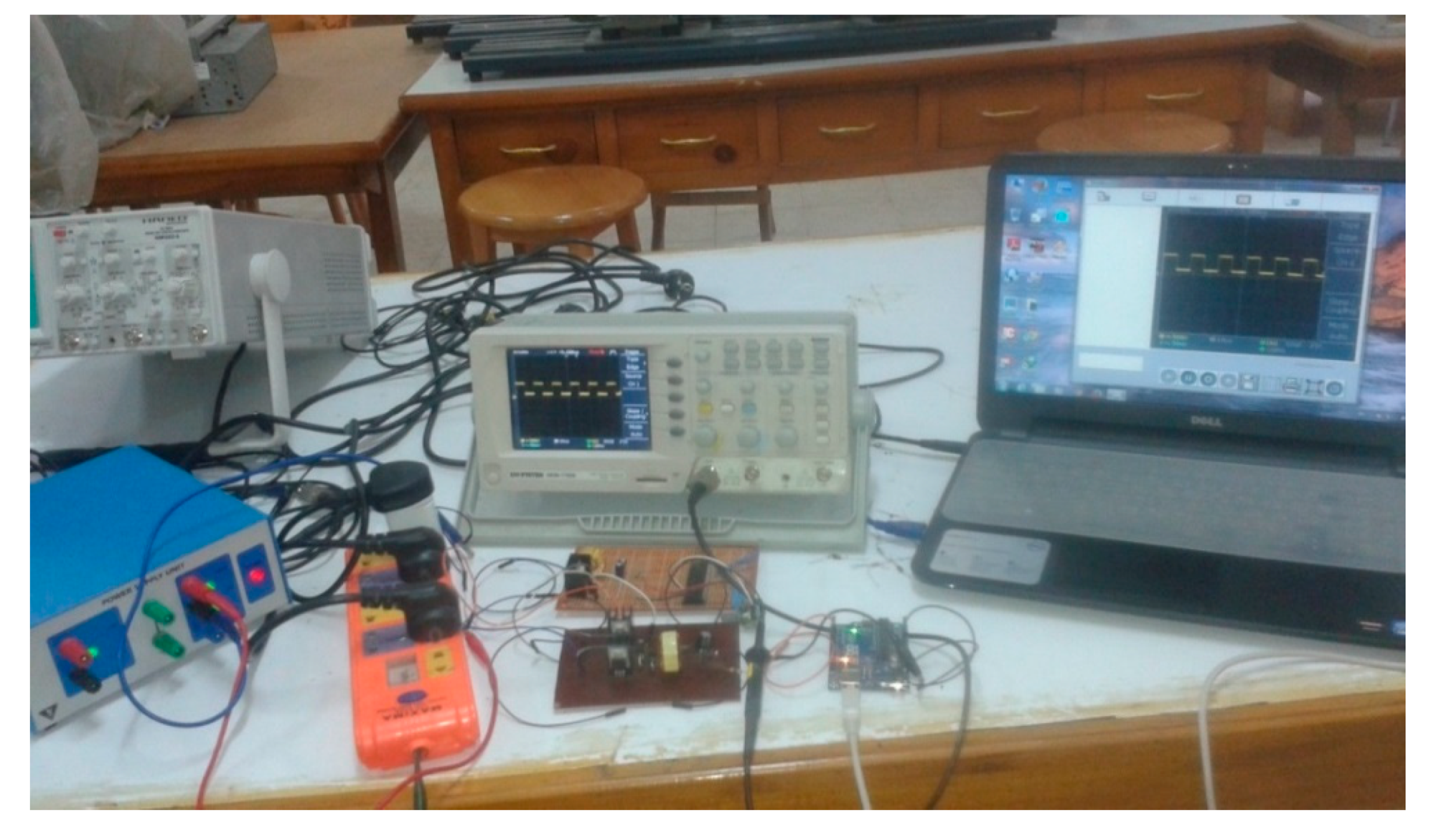
6. Experimental Results

The studied soft-switching circuit was implemented as a prototype to demonstrate the operation principle. The input voltage is taken from the PV module, monocrystalline, 250 W, Vmp = 30.7 V, Imp (max. power current) 8.15. A 600 V-40 A IGBT was used as a switch operating at a switching frequency of 40 kHz, and the duty cycle was changed to prove the operation technique. The gate signal was produced utilizing the PIC microcontroller, and thereafter, the PWM signal was delivered to an optocoupler TLP250 to drive the IGBT switch. Optical isolation was the major advantage of using this driver compared to other drivers. TLP 250 was used to implement fast switching of power devices and reduce associated switching power losses. TLP 250 as an optocoupler provides a very high isolation voltage. It can easily be interfaced with a microcontroller. The circuit parameters are listed in Table 1.
Figure 8 and Figure 9 show the waveforms of output voltage and current of two switches under different loading conditions. As shown, both the switches can turn on and turn off with zero-current soft switching. Subsequently, a reduction in the switching losses can be obtained, and an improvement in the efficiency of the converter can be achieved. Figure 10 shows the output voltage waveform at standard irradiance, i.e., 1000 W/m2, and full-load condition.
Figure 11 shows the measured efficiency of the proposed boost DC-DC converter. The developed circuit has better efficiency than the previously-developed [6] hard-switching converter. However, the maximum obtained efficiency is 97.1% at full load, i.e., 500 W; about a 3% improvement in efficiency is gained. The switching losses are about 5 W at a switching frequency 40 kHz. A photograph of the experimental setup hardware is shown in Figure 12. The PV array installation on the roof is shown in Figure 13.

7. Power Loss Analyses

The section presents a comparative analysis of previously-developed hard-switched and the proposed soft-switched converters. Analytical calculations are made to calculate the losses of components, voltage, power, and frequency of switching, and the increase in temperature due to the use of semiconductors devices. Figure 14 shows the power losses as a function of the input current. The compared power converters are realized and investigated experimentally. Figure 15 is used to analyze the dissipated losses in the two converters and each of their passive and active components. The power loss breakdown of the key components of the implemented converter is estimated. Figure 16 shows the losses breakdown (calculated value) at half- and full-loading condition of the proposed circuit.
Table 2 shows a comparison between the proposed circuit with different topologies used with PV modules. From this table, the proposed topology has a lower switching frequency and a higher efficiency.

8. Conclusions

A novel circuit with a soft-switching, high voltage gain boost DC-DC converter was investigated for PV module integration. The operation of the PV panels is analyzed to study the equivalent circuit of each model and its operation. The coupled inductor can be used to maximize the voltage gain of the proposed nonisolated boost PWM DC-DC converter according to the winding turns ratio. The control technique is discussed for the proposed ER-SC boost-type soft-switching DC-DC power converter. A simulation model of the PV system was developed using PSIM to validate the developed converter. Then, the results of the experimental work are introduced using a prototype converter. Losses and the efficiency of the prototype converter were measured.

Author Contributions

Conceptualization, H.A.Z. and K.S.; methodology, H.A.Z.; software, K.S.; validation, M.G.G., and H.A.Z.; formal analysis, K.S.; investigation, H.A.Z.; resources, K.S.; data curation, K.S.; writing—original draft preparation, M.G.G., and H.A.Z.; writing—review and editing, K.S.; visualization, H.A.Z.; supervision, K.S.; project administration, H.A.Z.; funding acquisition, M.G.G. All authors have read and agreed to the published version of the manuscript.

Funding

This research received no external funding.

Conflicts of Interest

The authors declare no conflict of interest.

References

  1. Lopez-Lapena, O.; Teresa Penella, M.; Gasulla, M. A New MPPT Method for Low-Power Solar Energy Harvesting. IEEE Trans. Ind. Electron. 2010, 57, 3129–3138. [Google Scholar] [CrossRef] [Green Version]
  2. Aghazadeh, H.; Kojabadi, H.; Yazdankhah, A. Stand-alone PV generation system with maximum power point tracking. In Proceedings of the 9th IEEE International Conference on Environment and Electrical Engineering, Prague, Czech Republic, 16–19 May 2010. [Google Scholar]
  3. Kadri, R.; Gaubert, J.-P.; Champenois, G. Nondissipative string current diverter for solving the cascaded dc–dc converter connection problem in photovoltaic power generation system. IEEE Trans. Power Electron. 2012, 27, 1249–1258. [Google Scholar] [CrossRef]
  4. Das, M.; Agarwal, V. Design and analysis of a high-efficiency dc–dc converter with soft switching capability for renewable energy applications requiring high voltage gain. IEEE Trans. Power Electron. 2016, 63, 2936–2944. [Google Scholar] [CrossRef]
  5. Choi, H.-S.; Cho, B.H. Novel zero current switching (ZCS) PWM switch cell minimizing additional conduction loss. IEEE Trans. Power Electron. 2002, 49, 165–172. [Google Scholar]
  6. Al Muzahid, M.; Ansari, M.; Salam, K.; Zaman, H. A High voltage gain DC-DC boost converter for PV cells. Glob. Sci. Technol. J. 2015, 3, 64–76. [Google Scholar]
  7. Zhu, Y.; Chen, M.; Lee, X.; Tsutomu, Y. A novel quasi-resonant soft-switching Z-source inverter. In Proceedings of the 2012 IEEE International Conference on Power and Energy (PECon), Kota Kinabalu, Malaysia, 2–5 December 2012; pp. 292–297. [Google Scholar]
  8. Sang-Hoon, P.; Gil-Ro, C.; Yong-Chae, J.; Chung-Yuen, W. Design and application for PV generation system using a soft-switching boost converter with SARC. IEEE Trans. Power Electron. 2010, 57, 515–522. [Google Scholar] [CrossRef]
  9. Yao, T.; Nan, C.; Ayyanar, R. A new soft-switching topology for switched inductor high gain boost. IEEE Trans. Ind. Appl. 2018, 54, 2449–2458. [Google Scholar] [CrossRef]
  10. Kim, Y.-H.; Shin, S.-C.; Lee, J.-H.; Jung, Y.-C.; Won, C.-Y. Soft-switching current-fed push-pull converter for 250-W AC module applications. IEEE Trans. Power Electron. 2014, 29, 863–872. [Google Scholar]
  11. Doo-Yong, J.; Young-Hyok, J.; Sang-Hoon, P.; Yong-Chae, J.; Chung-Yuen, W. Interleaved soft-switching boost converter for photovoltaic power-generation system. IEEE Trans. Power Electron. 2011, 26, 1137–1145. [Google Scholar]
  12. Sayed, K.H.; Kwon, S.-K.; Nishida, K.; Nakaoka, M. New DC rail side soft-switching PWM DC-DC converter with voltage doubler rectifier for PV generation interface. In Proceedings of the International Power Electronics Conference (IPEC-Hiroshima 2014—ECCE ASIA), Hiroshima, Japan, 18–21 May 2014. [Google Scholar]
  13. Jain, N.; Jain, P.K.; Joos, G. A zero voltage transition boost converter employing a soft switching auxiliary circuit with reduced conduction losses. IEEE Trans. Power Electron. 2004, 19, 130–139. [Google Scholar] [CrossRef]
  14. Moschopoulos, G.; Jain, P.K.; Liu, Y.-F.; Joos, G. A zero-voltage-switched PWM boost converter with an energy feedforward auxiliary circuit. IEEE Trans. Power Electron. 1999, 14, 653–662. [Google Scholar] [CrossRef]
  15. Ogura, K.; Chandhaket, S.; Ahmed, T.; Nakaoka, M. Boost chopper-fed ZVS-PWM DC-DC converter with parasitic oscillation surge suppression-based auxiliary edge resonant snubber. In Proceedings of the 25th International Telecommunications Energy Conference, Yokohama, Japan, 23 October 2003; pp. 20–26. [Google Scholar]
  16. Jung-Goo, C.; Ju-Won, B.; Geun-Hie, R.; Iouri, K. Novel zero-voltage-transition PWM multiphase converters. IEEE Trans. Power Electron. 1998, 13, 213–219. [Google Scholar] [CrossRef]
  17. Meneses, D.; Blaabjerg, F.; García, Ó.; Cobos, J.A. review and comparison of step-up transformer less topologies for photovoltaic AC-module application. IEEE Trans. Power Electron. 2013, 28, 2649–2663. [Google Scholar] [CrossRef] [Green Version]
  18. Li, W.; He, X. Review of nonisolated high-step-up dc/dc converters in photovoltaic grid-connected applications. IEEE Trans. Ind. Electron. 2011, 58, 1239–1250. [Google Scholar] [CrossRef]
  19. Kima, H.E.; Kima, J.K.; Kima, H.G.; Leea, K.; Kimb, J.; Yoob, D.; Shina, D. A high efficiency photovoltaic module integrated converter with the asymmetrical half-bridge flyback converter. Sol. Energy 2010, 84, 1376–1381. [Google Scholar] [CrossRef]
  20. Do, H.L. Analysis and implementation of a zero-voltage-switching cascade boost converter. Int. J. Electron. 2012, 99, 623–641. [Google Scholar] [CrossRef]
  21. Choi, H.-C.; Shin, H.-B. A new soft-switched PWM boost converter with a lossless auxiliary circuit. Int. J. Electron. 2006, 93, 805–817. [Google Scholar] [CrossRef]
  22. Iskender, I.; Genc, N. Design and analysis of a novel zero-voltage-transition interleaved boost converter for renewable power applications. Int. J. Electron. 2010, 97, 1051–1070. [Google Scholar] [CrossRef]
  23. Khan, A.; Batarseh, I. Zero-voltage switching boost converter for power factor correction. Int. J. Electron. 1995, 78, 1177–1188. [Google Scholar] [CrossRef]
  24. Sayed, K. A high efficiency DC-DC converter with LC resonant in the load-side of HFT and voltage doubler for solar PV systems. Int. J. Power Electron. 2017, 8, 232–248. [Google Scholar] [CrossRef]
  25. Sayed, K.; El-Zohri, E.; Mahfouz, H. Analysis and design for interleaved ZCS buck DC-DC converter with low switching losses. Int. J. Power Electron. 2017, 8, 210–231. [Google Scholar] [CrossRef]
  26. Sayed, K.; Gabbar, H. Supervisory control of a resilient DC microgrid for commercial buildings. Int. J. Process Syst. Eng. 2017, 4, 99–118. [Google Scholar] [CrossRef]
  27. Abdel-Salam, M.; Sayed, K.; Ahmed, A.; Amery, M.; Swify, M. Design, implementation and operation of a standalone residential photovoltaic system. Int. J. Power Energy Convers. 2017, 8, 47–67. [Google Scholar] [CrossRef]
  28. Sathyan, S.; Suryawanshi, H.M.; Singh, B.; Chakraborty, C.; Verma, V.; Ballal, M.S. ZVS–ZCS high voltage gain integrated boost converter for DC microgrid. IEEE Trans. Ind. Electron. 2016, 63, 715–721. [Google Scholar] [CrossRef]
  29. Hauke, B. Basic Calculation of a Boost Converter’s Power Stage. In Application Report, SLVA372C, 09; Texas Instruments: Dallas, TX, USA, 20 November; Revised January 2014.
  30. Sayed, K.; Hasanien, B. Current source ZCS PFM DC-DC converter for magnetron power supply. In Proceedings of the IEEE Middle East Power Systems Conference, MEPCON 08, Aswan, Egypt, 12–15 March 2008; pp. 464–469. [Google Scholar]
  31. Lee, H.-J.; Kim, Y.H. Analysis and design of a ZVT resonant boost converter using an auxiliary resonant circuit. Electronics 2019, 8, 466. [Google Scholar] [CrossRef] [Green Version]
  32. Jotham Jeremy, L.; Ai Ooi, C.; Teh, J. Non-isolated conventional DC-DC converter comparison for a photovoltaic system: A review. J. Renew. Sustain. Energy 2020, 12, 013502. [Google Scholar] [CrossRef]
  33. Moradisizkoohi, H.; Elsayad, N.; Mohammed, O. A soft-switched DC/DC converter using integrated dual half-bridge with high voltage gain and low voltage stress for DC microgrid applications. Inventions 2018, 3, 63. [Google Scholar] [CrossRef] [Green Version]
  34. Fares, A.M.; Klumpner, C.; Sumner, M. A novel modular multiport converter for enhancing the performance of photovoltaic-battery based power systems. Appl. Sci. 2019, 9, 3948. [Google Scholar] [CrossRef] [Green Version]
  35. Bassi, H.; Salam, Z.; Ramli, M.Z.; Sindi, H.; Rawa, M. Hardware approach to mitigate the effects of module mismatch in a grid-connected photovoltaic system: A review. Energies 2019, 12, 4321. [Google Scholar] [CrossRef] [Green Version]
  36. Sayed, K.; Abo-Khalil, A.G.; Alghamdi, A.S. Optimum resilient operation and control dc microgrid based electric vehicles charging station powered by renewable energy sources. Energies 2019, 12, 4240. [Google Scholar] [CrossRef] [Green Version]
  37. Viinamäki, J.; Suntio, T.; Kuperman, A. Grid-forming-mode operation of boost-power-stage converter in PV-generator-interfacing applications. Energies 2017, 10, 1033. [Google Scholar] [CrossRef] [Green Version]
  38. Suntio, T.; Messo, T.; Aapro, A.; Kivimäki, J.; Kuperman, A. Review of PV generator as an input source for power electronic converters. Energies 2017, 10, 1076. [Google Scholar] [CrossRef] [Green Version]
Figure 1. (a) Circuit diagram of the soft-switched boost converter proposed in [6]. (b) The soft-switching PV inverter proposed in [7]. (c) Zero-voltage-transition (ZVT) circuit proposed in [13]. (d) Zero-voltage soft-switching boost converter with auxiliary edge-resonance snubbers proposed in [15]. (e) Boost PWM ZVT circuit proposed in [16].
Energies 13 00749 g001
Figure 2. Proposed soft-switched ER-SC boost DC-DC converter.
Energies 13 00749 g002
Figure 3. Operating waveforms.
Energies 13 00749 g003
Figure 4. Equivalent circuits of operation intervals.
Energies 13 00749 g004
Figure 5. Voltage and current output of the proposed DC-DC converter at a 0.5 duty cycle.
Energies 13 00749 g005
Figure 6. Equivalent S-domain of the resonant circuit.
Energies 13 00749 g006
Figure 7. Soft-switching DC-DC boost converter block diagram.
Energies 13 00749 g007
Figure 8. Waveforms of voltage and current of switches S1 and S2 at Po = 200 W.
Energies 13 00749 g008
Figure 9. Operating waveforms of voltage and current of switches S1 and S2 at Po = 500 W.
Energies 13 00749 g009
Figure 10. Output voltage at standard irradiance and full-load condition.
Energies 13 00749 g010
Figure 11. Efficiency which measured for the prototype DC-DC converter.
Energies 13 00749 g011
Figure 12. Hardware installation of the experimental setup.
Energies 13 00749 g012
Figure 13. The PV array installation on the roof (250-W, 72-cell PV module)
Energies 13 00749 g013
Figure 14. Calculated losses in each component of the proposed PV converter.
Energies 13 00749 g014
Figure 15. Losses comparison between the hard-switched and proposed converter.
Energies 13 00749 g015
Figure 16. Breakdown losses. (a) Using half-load (Po = 250 W); and (b) Using full-load (Po = 500 W).
Energies 13 00749 g016
Table 1. PV module prototype parameters.
Parameter Value, Unit
Rated output power Po500 W
Input voltage Vin30 V
Output voltage Vo100 V
Boost inductor Lr = L1 = L2900 μH
Mutual inductance M770 μH
Resonant capacitor Cr60 nF
Variable load resistor Ro20 Ohm
Output smoothing capacitor C1 = C2500 μF
Switching frequency40 kHz
Photovoltaic ModuleMonocrystalline, 250.0 Watt, Vmp = 30.7 V, Imp = 8.15 A
Table 2. Comparison with other existing topologies.
Parameter ProposedRef. [6]Ref. [7]Ref. [8]Ref. [3]
Input voltage30150–230100–200 V90–25623
Output voltage10038030040030
Voltage gain32.531.5–31–41.5
Switching frequency40 k30 k100 k100 kHz100 k
Rated power500 W700 W100025010–60 W
Efficiency9796979592–94%

