Article

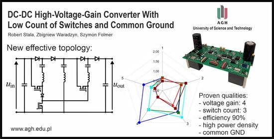
DC-DC High-Voltage-Gain Converters with Low Count of Switches and Common Ground

Department of Power Electronics and Energy Control Systems, Faculty of Electrical Engineering, Automatics, Computer Science and Biomedical Engineering, AGH University of Science and Technology, al. Mickiewicza 30, 30-059 Krakow, Poland
*
Author to whom correspondence should be addressed.
Energies 2020, 13(21), 5657; https://doi.org/10.3390/en13215657
Submission received: 1 September 2020 / Revised: 29 September 2020 / Accepted: 26 October 2020 / Published: 29 October 2020

Abstract

:
This paper presents a new concept and research results of DC-DC high-voltage-gain, high-frequency step-up resonant converters. The proposed topologies are optimized towards minimizing the number of switches and improvements in efficiency. Another relevant advantage of such type of converters is that they have a common input and output negative point. The proposed converters are based on the resonant switched-capacitor voltage multiplier circuit, and that is why they are compared with a classic converter from this family. The included results show the operating principle, possible switching methods with the consideration of their impact on the voltage gain level, as well as the voltage and current ripples. The operating concepts and analytical calculations are confirmed by simulation and experimental results.

Graphical Abstract

1. Introduction

Switched capacitor (SC) circuits can be effectively used in power electronic converters [1]. The significant advantages of SC-based DC-DC power converters are high-voltage-gain, low volume, and quasi inductiveless design. To achieve oscillating currents, low-volume inductors can be used in those converters. They can be designed as air-chokes, or even be based on parasitic inductances of the circuits, resulting in a decrease in the weight of the converter. The design without ferrite chokes allows for the use of the converter in high ambient temperature and/or with a low-volume heat sink.
SC DC-DC converters represent one of the classes of non-isolated step-up converters [2,3,4]. Nowadays, there are a significant number of applications where isolated DC-DC step-up converters are required [3], due to technical reasons and safety requirements. However, various kinds of non-isolated converters are extensively developed as well. One of the prospective applications for non-isolated DC-DC step-up converters proposed in the literature [5,6,7,8,9,10] are photovoltaic (PV) systems. High step-up DC-DC converters are often required in grid-connected PV systems to transfer the energy from a low-voltage PV source to the grid [5,6]. In transformerless PV systems [7,8], as well as in microinverters [9], dual-stage DC-AC converters are one of the investigated solutions.
The SC step-up DC-DC converter could be a competitive solution to the switch-mode boost converter. An example of such an idea is presented in Reference [10]. The non-isolated step-up converter can be used not only for a single stage supply, but as a part of a system composed of series-connected converters as well. In such systems, isolation can be implemented in another stage of conversion, e.g., by using a series resonant converter [6,11].
High-voltage-gain in SC-based DC-DC converters can be achieved by applying a suitable topology concept. In References [12,13,14], an SC voltage multiplier (SCVM) has been presented. It is a series-parallel converter in that a high-voltage-gain can be obtained, as it is proportional to the number of switching cells. The advantage of an SCVM is its modular topology; however, the number of required transistors is relatively high. Series-parallel SC converters have also been presented in recent publications [15,16]. In Reference [15], a converter with regulated voltage gain has been discussed. This device utilizes three switches, which means that the voltage gain can reach three. Reference [16] has presented a very effective method that allows the switch count in high-gain series-parallel converters to be decreased. However, the converter presented in Reference [16] does not have a common input and output negative point, and the output voltage is asymmetrically divided. In Reference [17], a converter that combines Dickson-based and ladder SC converter concepts has been presented. In the proposed topology, high-voltage-gain is achieved with limited voltage and current stresses on the switches. The Dickson-based SC concept has also been used in the converter presented in Reference [18] that is composed of an SC part and an interleaved boost converter. The converter achieves a very high-voltage-gain with the output voltage regulation and soft switching operation, using four switches and seven diodes. In Reference [19], high-voltage-gain is achieved in a converter with switched-capacitor and switched-inductor networks. A concept of a family of converters composed of a boost stage and switched-capacitor-inductor cells has been presented in Reference [20]. This increases the voltage gain of the converter significantly with favorable voltage stress levels, efficiency, and component count. References [21,22,23,24] have demonstrated high-voltage-gain multilevel converters based on typical multilevel converter concepts. When we take into consideration the number of the utilized components and the reached voltage gain, the multilevel SC converters can be more beneficial in comparison to the SCVMs. The converter described in Reference [21] is based on a modified classic multilevel SC topology; however, it is composed of a significant number of switches. In Reference [22], an improvement in the operation of the multilevel resonant SC converter (MRSCC) has been proposed. The MRSCC makes it possible to operate with high-voltage-gain and limited voltage stress on the switches with the ability of bi-directional energy transfer. In Reference [23], a multilevel structure has been achieved in the converter with two switches and circuits composed of diodes and capacitors. The converter can operate with zero voltage switching (ZVS) and voltage regulation. In Reference [24], a DC-DC bidirectional SC converter has been presented that improves the total device power ratings in comparison to the multilevel modular capacitor clamped converter (MMCCC) and well-established flying-capacitor converters.
One of the major issues of the SC converters is a large number of switches used in the topology. This problem can be solved by the concepts of cascaded or series systems composed of SC units [25,26] or by new concepts of topologies [16,27,28]. In the concept for the switch count reduction presented in Reference [26], a high-power converter has been analyzed in a multi-section topology. The converter is composed of the typical SCVM sections separated by LC filters. According to this concept, a significant reduction in the number of switches has been achieved. However, an increased number of passive components are utilized as LC filters between the sections in the multi-section converters [26]. The problem of the switch count reduction in an SCVM converter has been analyzed in Reference [29], where the charging of the switched capacitors is controlled by a single switch. For high-voltage-gain, the system is significantly simplified. The design of such a cost-effective converter should assume a much higher current stress of the switch that controls the charging of the switched capacitors.
The converters proposed in this paper are optimized towards a low count of transistors (and they are called Low Count of Transistors Switched Capacitor Voltage Multipliers—LCSCVMs). The basic concept of the topology and operation assumes that every second cell has no transistors whatsoever, but the utilization of all the switched capacitors remains possible, and the effect of voltage gain is comparable to that of the multipliers (SCVMs) presented in Reference [13,14]. Furthermore, the optimized concept is introduced into the cost-effective topology presented in Reference [29], which gives a new relevant converter. Taking into consideration the count of switches, SC converters, such as the SCVM [20], may not be in competition with the LLC converters or other established topologies. However, the concepts proposed in this paper demonstrate a development of the SC topologies towards a significant decrease in the number of switches. One of the converters presented in this paper requires only three switches, which is below the number of transistors used in a full-bridge LLC converter. Other advantages of the SC converters, such as: high gain, high power density and low weight (no transformer or bulky choke), fast dynamic response [3], ability for operation in high temperature (no ferrites), and simple control, can make them an alternative solution for existing topologies intended for high-voltage-gain non-isolated DC-DC conversion. SC-based topologies can be suitable for the miniaturization of converters that can be applied in emerging power electronics applications, such as wearable technology.
For the operational parameters of an SC converter, the switching strategy applied for a given topology can be essential, which has been demonstrated in Reference [14]. For the optimization purposes analyzed in this paper, various switching strategies are proposed for the new topologies. This makes it possible to determine the advantages of the presented topologies, also taking into consideration a variety of qualities, other than the count of switches.
The proposed converters are nearly pure switched-capacitor circuits, where a vast majority of energy is transferred via capacitors rather than inductors. The resonant inductors are used to achieve oscillatory currents. The inductors can be designed as air chokes, which reduces the weight of the converters and allows them to work in higher temperatures. However, another trend in the development of very high-voltage-gain converters can be observed in the literature. The concept presented in Reference [30] is based on coupled inductor (CI) converters that achieve good parameters such as voltage ratio, efficiency, low number of switches, or low voltage stress on switches. Notwithstanding, such converters use chokes and, therefore, differ from the presented SC-based concept regarding admissible ambient temperature of operation, weight, and volume. The design comparison can be analyzed in particular case studies.
In this paper, the qualities introduced by the new topologies will be compared with those of a classic SCVM and of other converters discussed in recently published papers.
The paper is organized as follows. Section 2 demonstrates two proposed topologies of the SC converters and presents the principles of their operation. For both converters, switching strategies are analyzed. The discussion is supported by the results of computer simulations of their operation in five cases of switching strategies. Moreover, with the use of the simulation results, a number of parameters of the converters operating under various switching strategies are compared as well. Section 3 contains efficiency models of the proposed converters that demonstrate their efficiency as a function of their parameters. Section 4 presents the laboratory setup and the experimental verification of its operation, including the efficiency of the converter. All the research results are concluded in Section 5.

2. Operating Principle of the Converters

The operating principle of the converters in Figure 1 is similar to that of other SC multipliers, and is based on the charging and discharging of the switched capacitors in consecutive stages (time intervals). However, various switching strategies can be proposed for the new converters, which creates differences in their parameters. In the SCVM, as well as in the case of the converters proposed in this paper, the switched capacitors are recharging in resonant circuits composed of a switched capacitor and a low-volume resonant inductor. This creates ZCS (zero current switching) operating conditions, and limits the current flow between the capacitors and the voltage source connected in parallel.
The main difference between the topology of the proposed converters and the classic SCVMs is that in the former case, an LC circuit that is not a part of a traditional cell is used, usually consisting of a diode and two transistors [13]. This circuit is charged using the energy of the input source and the electric charge of the switched capacitor that is the nearest to the input source. Then, the middle capacitor is discharged to the output capacitor or to the switched capacitor nearer to the output. Its function is to increase the output voltage and the amount of converted power, simultaneously maintaining the same value of the input voltage and the same cell number as in the case of a typical SCVM.
The LCSCVMa (Figure 1a) offers a larger number of strategies than the LCSCVMb (Figure 1b), due to the possibility of independent control of switches S1 and S3. The basic switching strategies can be composed of 2, 3, or 5 stages.

2.1. Switching Strategy Concepts for the LCSCVMa

Table 1 presents three switching strategies for the LCSCVMa, and Figure 2, Figure 3, Figure 4 and Figure 5 depict the corresponding simulation waveforms.
To characterize the switching strategies, Table 1 contains the idealized control logic waveforms of the transistors (signals S1 to S4), as well as the description of the particular operation stages. Dead times have been neglected in Table 1, but they have been taken into account in the simulations and experiments. Capacitor C2 (Figure 1) is not referred to as a switched capacitor. The maximum switching frequency (strategy C3) is defined as:
f S max = 1 2 T p u l s e
where Tpulse is the sum of the duration time T0/2 of a single current pulse of any transistor and the dead time td (any period of time denoted as 1–5 in Table 1),
T 0 = 1 f 0 = 2 π L C
and L = L1 = L2 = L3, C = C1 = C2 = C3 (Figure 1).
All the simulation results were obtained for the following parameters: Uin = 50 V, Ln = 620 nH, Cn = 1.47 μF, f0 = 166.7 kHz, Tpulse = 4.2 μs (fSmax = 119 kHz), Cout = 100 μF, Pout = 200 W (n = 1, 2, 3). A resistance of 100 mΩ has been inserted into each branch as an equivalent to parasitic resistances. The time period Tpulse, as well as the duty cycle of the switching signals of the transistors, remain constant in each switching strategy. The selection of the switching frequency depends on the power of the converter, achievable resonant inductance, and switching losses [13]. This parameter, as well as the others, can be fixed in the following steps. In the ZCS mode, the SC converters’ transistors do not operate in the ZVS mode, and during their turn-ons, the output charge is shorted (Coss losses). The limit of Coss losses determines the switching frequency of the transistors taking into consideration their type and voltage stresses. The oscillation frequency should be nearly equal to the switching frequency to minimize conduction losses [13]. This frequency depends on the product of LnCn, and allows to select Cn for a known value of Ln. The maximum power of the converter depends on capacitance Cn and the switching frequency [13], and it should be higher than or equal to the rated power for the selected parameters. The simulation results presented in this section have been obtained with the use of ICAP/4 simulation package based on the IsSpice4 simulator.

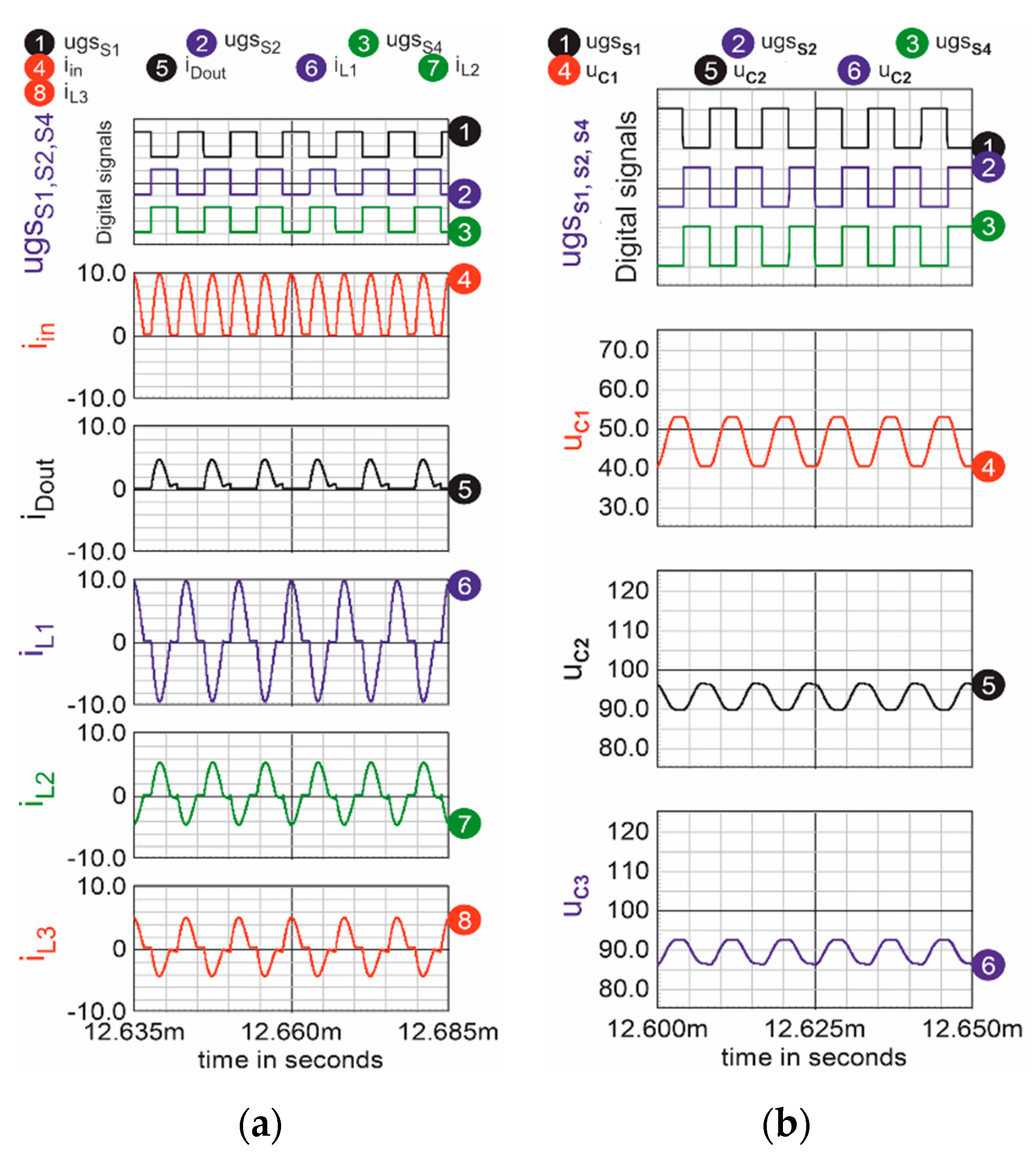
2.1.1. Simulation Results of the Switching Strategy C1

Figure 2 presents steady-state simulation waveforms of the LCSCVMa controlled according to strategy C1. From all the results, it can be seen that the switched capacitors are recharged by oscillatory currents and each stage of the switching is longer than the half-period of the oscillations.
The entire switching cycle is composed of five stages (Table 1). According to the principle of operation, turning on switches S1 and S3 involves the charging of the switched capacitors C1 and C3. Capacitor C3 is being charged from capacitor C2 of the internal branch whose voltage is going down in this stage. The diode D2 remains turned off, as uC2 > uC1 and uC2 > uin (Figure 2). In the next stage, switch S2 is turned on, and capacitor C2 is being charged from the source uin and capacitor C1 connected in series with it. The charging of the output capacitor, from capacitors C2 and C3 connected in series, occurs in the next stage when the switch S4 is turned on. At the same time, capacitor C1 is being charged from the source. In the next two stages, capacitor C2 and capacitor Cout are being charged, consecutively.
The advantage of this switching strategy is reducing the number of the performed switching operations, which leads to switching losses limitation. In three of five stages of the switching period, only one switch is affected.
The input current has various values in each switching state, which is a drawback of this strategy. Therefore, a low-frequency component fS = fac-in = fSmax/2.5 appears in current iin, as well as in all other currents and voltages in the circuit. Using this kind of switching requires using a large input filter and a large output capacitor. From the standpoint of the components’ volume and input current filtering, this strategy is not favorable.
The output voltage used for the voltage gain calculation in relation (3) has been measured as the average value of the waveform presented in Figure 3 together with the output current. Further results, given in Equations (4)–(7), were obtained in the same manner.
In this strategy, the measured average value of the output voltage of the converter equals Uout = 178 V. For the input voltage of the converter Uin = 50 V (maintained by the voltage source in simulations), the voltage gain of the converter under switching strategy C1 equals:
G U C 1 = U out U in = 178.0 50.0 = 3.56

2.1.2. Simulation Results of the Switching Strategy C2

Figure 4 presents simulation waveforms in the LCSCVMa controlled according to strategy C2. In this strategy, each switching period consists of three stages. The first two switching stages correspond to those in strategy C1. In the third stage, only transistor S3 is on. The last two stages of strategy C1 do not occur here, and capacitor C2 is charged and discharged only once in a switching period. The number of the switching operations is lower in comparison to that in strategy C1. The spectrum of currents and voltages shows more favorable qualities in strategy C2 versus C1, as the 50 kHz components are not present (the lowest frequency is 75 kHz).
In this strategy, the measured average value of the output voltage of the converter equals Uout = 177 V. For Uin = 50 V, the voltage ratio is
G U C 2 = U out U in = 177.0 50.0 = 3.54

2.1.3. Simulation Results of the Switching Strategy C3

Figure 5 presents simulation waveforms in the LCSCVMa controlled according to strategy C3. In this strategy, there are only two stages. In the first stage, the charging of the switched capacitors takes place (switches S1 and S3 are turned on). During the second stage, the output capacitor and C2 are being charged (with switches S2 and S4 turned on).
In this strategy, each switch operates with a much higher frequency than in the case of strategies C1 and C2. This brings an improvement in the spectrum of the currents and voltages, as the lowest frequency is 120 kHz. It is favorable from the passive components volume optimization standpoint.
In strategy C3, the measured average value of the output voltage of the converter equals Uout = 185 V, and for Uin = 50 V, the voltage ratio is
G U C 3 = U out U in = 185.0 50.0 = 3.7

2.2. Switching Strategy Concepts for the LCSCVMb

The LCSCVMb converter is simpler than the LCSCVMa, and contains three switches only. There is only one stage of charging the switched capacitors, realized by the switch S1, and two possible stages of discharging them, controlled by switches S2 and S3. This creates two switching strategies for this converter, which are presented in Table 2. Figure 6 and Figure 7 depict simulation waveforms of the LCSCVMb controlled according to these strategies.

2.2.1. Simulation Results of the Switching Strategy C4

Figure 6 presents simulation waveforms of the LCSCVMb controlled according to strategy C4. The current and voltage waveforms in strategy C4 are nearly identical with those in strategy C2.
In this strategy, the measured average value of the output voltage of the converter equals Uout = 172.1 V, which yields (for Uin = 50 V):
G U C 4 = U out U in = 172.1 50.0 = 3.44

2.2.2. Simulation Results of the Switching Strategy C5

Figure 7 presents simulation waveforms for the LCSCVMb controlled according to strategy C5. The current and voltage waveforms of the strategy C5 are nearly identical with those in strategy C3.
In this strategy, the measured average value of the output voltage of the converter equals Uout = 181.4 V. For Uin = 50 V, the voltage ratio is:
G U C 5 = U out U in = 181.4 50.0 = 3.63

2.3. Comparison among the Topologies and Switching Strategies

In Section 2.1 and Section 2.2, a significant number of waveforms are presented for the particular strategies. The differences in the waveforms of the currents and voltages are clear, but to compare the concepts of the converters and the switching strategies, the following parameters will be taken into consideration and presented in charts:
  • Number of components,
  • Voltage gain,
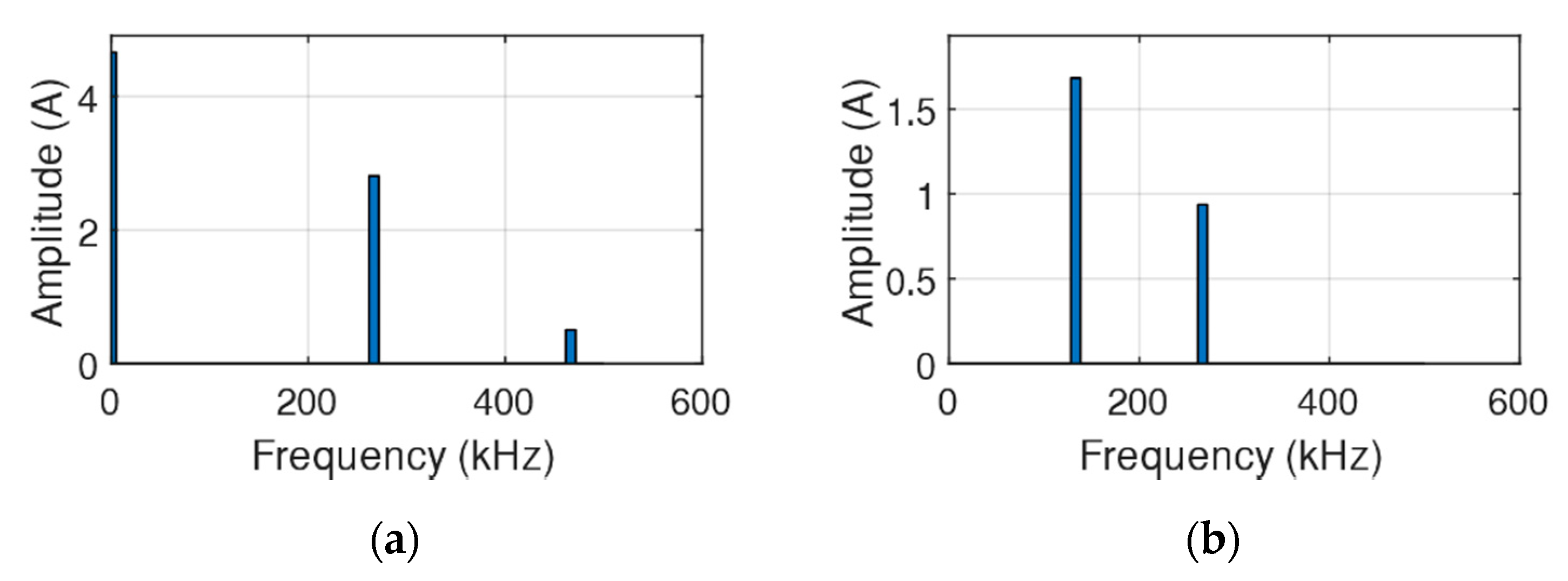
  • The lowest frequency in the input current (fac_in),
  • The lowest frequency in the output current (fac_out),
  • Voltage pulsation on capacitors (UC1p-p, UC2p-p, UC3p-p),
  • rms values of inductor currents (IL1_rms, IL2_rms, IL3_rms),
  • Maximum values of inductor currents (IL1_max, IL2_ max, IL3_ max),
  • Symmetry of inductor currents (Sym_iL).
The data are presented in Table 3, where the parameters of the SCVM (on the basis of Reference [14] for an appropriate strategy) are included as well.
Figure 8, Figure 9 and Figure 10 present a comparison between the values of parameters of the discussed converters, and the corresponding parameter of the SCVM.
In Figure 8, the coefficients 0.06 and 0.4 are used respectively, to better visualize the undesired output voltage decrease in regard to the theoretical value of 200 V, and the lowest frequencies in the input and output current of the discussed converters compared to those in the SCVM. In each case, a lower value on the graph is better.
From the chart presented in Figure 9a, it follows that the lowest peak-to-peak (p-p) voltages, in all the strategies, are equal the voltage across capacitor C3. Moreover, the strategies C3 and C5 show the lowest p-p voltages for all the internal capacitors (C1C3). Figure 9b demonstrates that the currents of inductor L3 are the lowest, and the strategies with the lowest inductor currents are C3 and C5.
The same qualities are visible in charts presented in Figure 10, which clearly demonstrate that the parameters of strategy C4 are nearly the same as those of strategy C2. The same refers to strategies C5 and C3.
The LCSCVMa and LCSCVMb converters can be further extended to units of higher voltage gain, similarly as in the case of the converters presented in References [13,22,25,26,29]. Taking into consideration the number of switches and diodes, as well as the frequency of the input current, both the proposed converters are very attractive for high-voltage-gain (Table 4). It should be noticed that the converter extension is very effective in the case of the LCSCVMb concept. For voltage gain GU = 8, it requires only four switches, which is an excellent result in comparison to other pure SC converters. Other parameters such as voltage stresses on the switches can be found in the literature.

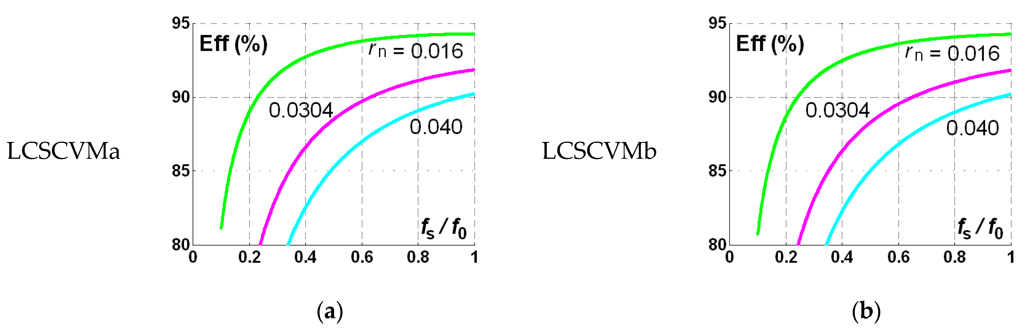
3. Efficiency Model of the LCSCVM Converters

The analysis below concerns the LCSCVMa operating under the strategy C3 (Table 1) and LCSCVMb operating under the strategy C5 (Table 2). In both cases, there are two stages of operation. Figure 11 depicts the current paths in the LCSCVMa. In the LCSCVMb, the switch S1 conducts the sum of currents iL1 and iL3 in the stage 1, whereas the current paths in the stage 2 are the same as in the LCSCVMa.
Assuming ideal power electronic switches, and a constant value of the input (Uin) and the output (Uout) voltage, as well as neglecting parasitic resistances and voltage drops across the power electronic devices, the currents in the stage 1 (Figure 11a) can be described as follows:
i L 1 ( t )   =   i C 1 ( t )   =   U in   U C 11 ρ   sin ω 0 t   =   I 1 m   sin ω 0 t
i L 3 ( t )   =   i C 3 ( t )   =   U in   U C 11 2 ρ   sin ω 0 t =   I 1 m 2   sin ω 0 t
i L 2 ( t )   =   i C 2 ( t )   =   i L 3 ( t )
With the characteristic impedance and the angular resonant frequency given by
ρ   =   L / C ,   ω 0   =   1 / L C
where UC11 is the initial voltage across capacitor C1, and I1m and I2m/2 are the current amplitudes. Equation (8) presents the current of a typical series LC circuit supplied from a voltage source, and Equation (9) was obtained also taking into account the initial values of the capacitor voltages.
The values of the passive components depend on the assumed nominal power (Pnom), switching frequency (fS), and the volume of the resonant inductor. The values of time Tpulse (1), and finally T0 (2) and ω0 (11), are assumed taking into account the limit of the switching losses in the converter. The capacitance of the switched capacitors is determined by the charge required to be transferred in a single switching pulse. The maximum power of the SCVM-type converter is achieved when the switched capacitors are fully discharged in a switching cycle (and then charged to the voltage equal to 2Uin). This determines the minimum capacitance, which in the SCVM composed of n switching cells is defined as follows:
Cmin= 2nfSUin2/Pnom.
In a quasi inductiveless SCVM-type converter, the value of resonant inductance (L) is very small (L can be designed as a PCB air choke). Therefore, to achieve the assumed switching frequency, the capacitance of the switched capacitors can be selected considerably bigger than Cmin (as in the case of the experimental setup presented in this paper). In the stage 2 (Figure 11b), the currents of capacitors C1C3 and inductances L1L3 have the same values (Equations (8)–(10)) as in the stage 1, but with the opposite signs. The voltages across the capacitors C1, C2, and C3 in the stage 1 are given by
u C 1 ( t )   =   ( U in   U C 11 )   ( 1     cos   ω 0 t )   +   U C 11
u C 2 ( t ) =   ( U in   U C 11 ) 2   ( 1     cos   ω 0 t )   +   U C 21
u C 3 ( t ) =   ( U in   U C 11 ) 2   ( 1     cos   ω 0 t )   +   U C 31
where UC21 and UC31 are the initial voltages across capacitors C2 and C3, respectively.
In the stage 2 (Figure 11b), the expressions for voltages have similar forms with appropriate signs and initial values.
Based on the formulas mentioned above, all the voltage initial values and the output voltage can be computed as a function of UC11. For example, we obtain
U out   =   5 U in   U C 11
UC11 can be calculated taking into account (8) and the following relation
I in - av   =   I L 1 av   =   2 π   I 1 m f S n   =   P in U in
U C 11   =   U in     π   ρ   P in 2 f Sn U in
where
f Sn =   f S / f 0
From Equations (16) and (18), we have
U out   =   4 U in +   π   ρ   P in 2 f Sn U in
In practical converters, there are voltage drops across the circuit elements like the diodes and the transistors, which result in a variation of the output voltage with power and frequency.
The efficiency of an SCVM-type converter is determined by the resistances of its components, voltage drops on the diodes and transistors, the input voltage, power, and by the relation between the switching period TS and period T0 (2), which can be expressed by fSn (19). Therefore, it is necessary to calculate the average and rms values of the currents. It is assumed that transistors S1 and S3 are IGBTs, and S2 and S4 are MOSFETs.
I D 1 av =   I D 2 av =   I L 1 av 2   =   1 π   I 1 m f S n   =   P in 2 U in ,   I D 3 av =   I D out - av =   I L 2 av 2   =   I L 3 av 2   =   I L 1 av 4   =   P in 4 U in
  I S 2 =   1 2 I 1 m f Sn   =   π P in 4 U in f Sn ,   I S 4 =   1 4 I 1 m f Sn   =   π P in 8 U in f Sn
For the LSCVMa, we have:
I S 1 av =   I D 1 av   =   P in 2 U in ,   I S 3 av =   I D 3 av =   P in 4 U in
Conduction losses, ΔPc, in both converters are
Δ P c   =   k r k I S k 2 +   l Δ U D l I D l av +   m Δ U S m I S m av + n r T I n 2
where rk denotes the total resistance of the branch with MOSFET transistor Sk (k = 2, 4), including the resistance of the transistor. ΔUDl is the voltage drop across diode Dl, ΔUSm is the voltage drop across IGBT transistor Sm, rT is the resistance of each circuit with an IGBT transistor, and In is its rms current.
It is assumed that the voltage drops across the devices remain constant in the conducting state.
We assume that all the resistances and voltage drops are the same, i.e.
r 2   = r 4   =   r ,   Δ U S 1   =   Δ U S 2   = Δ U S ,   Δ U D 1   =   Δ U D 2   =   Δ U D 3   =   Δ U D 4   =   Δ U D out   =   Δ U D
The efficiency of the LSCVMa converter can be calculated as follows. The resistive losses in the circuits containing IGBTs are:
Δ P c 2   = r T I L 11 2   +   2 r T I L 31 2   = 3 π 2 P in 2   r T 32 U in 2 f Sn
Taking (21)–(26) into account, the conduction losses can be presented as
Δ P c   =   5 π 2 P in 2   r 64 U in 2 f Sn   +   3 π 2 P in 2   r T 32 U in 2 f Sn   +   3 P in 2 U in ( Δ U D   +   1 2 Δ U S )
The turn-off switching loss is zero, due to the ZCS switching. However, there is a turn-on switching loss, associated with charging and discharging the transistors’ output capacitances. The total switching power loss, ΔPsw, is
Δ P sw =   Δ W sw f S   =   Δ P sw 0 f Sn
where ΔWsw is the energy lost at turn-on in the transistor’s resistances in a single switching cycle, and ΔPsw0 = ΔWsw·f0 is power loss at resonant frequency. A way of calculating these losses is presented in Reference [31].
The efficiency is (Equations (27) and (28))
η =   1     Δ P c P in     Δ P sw P in   =   1   5 π 2 P in 2 r 64 U in 2 f Sn     3 π 2 P in 2 r T 32 U in 2 f Sn   3 P in 2 U in ( Δ U D   +   1 2 Δ U S )     Δ W s w f S P in
Introducing normalized quantities:
r n   =   r U in 2 / P in ,   r T n   =   r T U in 2 / P in ,   Δ U D n   =   Δ U D U in ,   Δ U S n   =   Δ U S U in ,   Δ P sw 0 n   =   Δ P sw 0 P in
We can simplify the efficiency formula to the form
η   =   1     5 π 2 r n 64 f Sn     3 π 2 r T n 32 f Sn     3 2 ( Δ U D n   +   1 2 Δ U S n )     Δ P sw 0 n f Sn
The efficiency of the LSCVMb can be calculated with the use of the following components:
I S 1 av =   I D 1 av   +   I D 3 av   =   3 P in 4 U in ,   I D 4 av =   I D 1 av = P in 2 U in
where D4 is the LSCVMb additional diode (Figure 1b).
Conduction losses, ΔPc, of LSCVMb are as follows:
Δ P c = 5 π 2 P in 2 r 64 U in 2 f Sn + 3 π 2 P in 2 r T 32 U in 2 f Sn + P in U in ( 2 Δ U D + 3 4 Δ U S )
and the efficiency of the LSCVMb is
η   =   1     5 π 2 r n 64 f Sn     3 π 2 r T n 32 f Sn     ( 2 Δ U D n +   3 4 Δ U S n )     Δ P sw 0 n f Sn
It can be seen from (30), (31), and (34) that the impact of the voltage drops across the diodes on the efficiency depends only on the ratio of these voltage drops to the supply voltage. The impact of the losses in the resistances is more complex. They increase with rising resistances and rising power, and decrease with rising input voltage and frequency fS. Switching losses are proportional to switching frequency fS.
The relationship between the efficiency and normalized frequency fSn = fS/f0 for three values of rn (30): 0.016, 0.0304, and 0.040, ΔUDn (30) = 0.008 for the LCSCVMa and the LCSCVMb is shown in Figure 12. The value of rn = 0.0304 corresponds to, e.g., Uin = 50 V, Pin = 200 W, L = 500 nH, C = 1.5 μF, r = 380 mΩ, and ΔUDn is equal to 0.008 for, e.g., ΔUD = 0.40 V and Uin = 50 V. The value of relative switching losses Psw0n (30) = 0.0101 (Figure 12b) is valid, e.g., for ΔWsw (28) = 11 μJ, f0 = 183.8 kHz, and Pin = 200 W. The efficiency of the LCSCVMb is slightly lower. In both cases, it increases with increasing normalized frequency, fSn, and strongly depends on the circuit parasitic resistances. Therefore, it is important to minimize them, and use transistors with low values of RDS(on) and VCE(on).
The efficiency can be computed in a similar way for the other switching strategies. However, the calculations will be more complex in the case of the strategies with more than 2 stages.

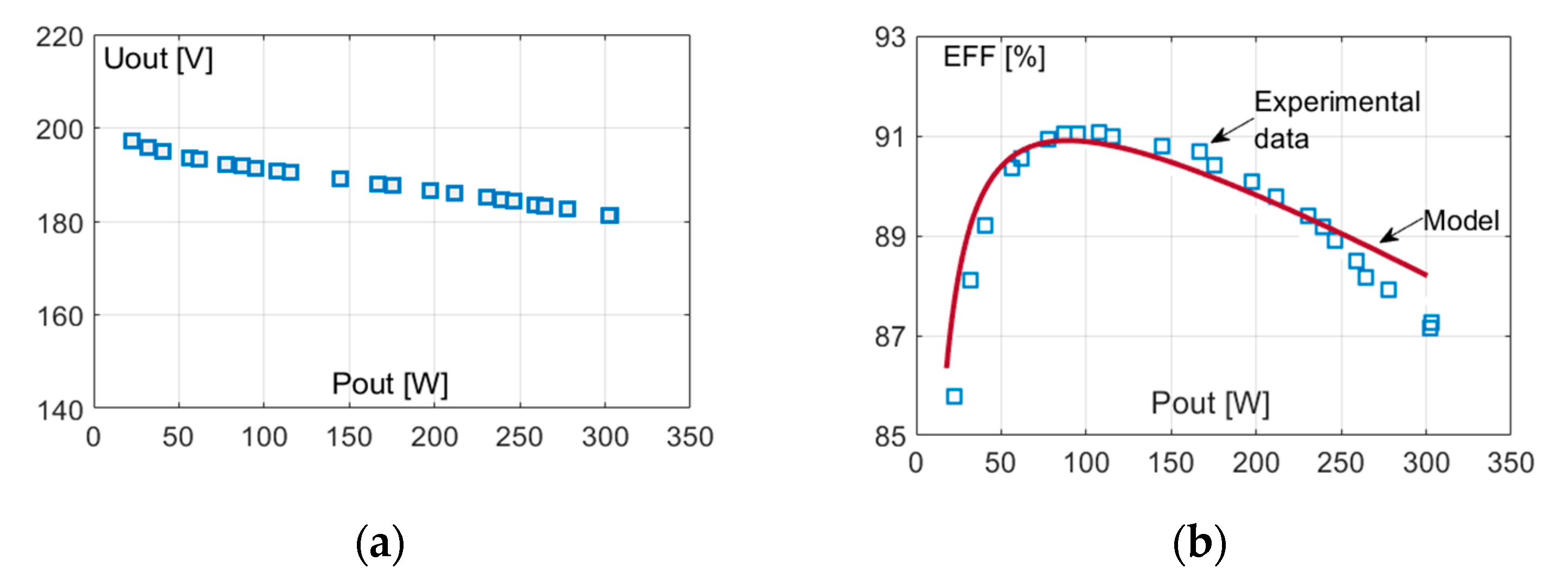
4. Experimental Verification

This chapter presents the experimental results of the LCSCVMb converter operation. All the tests were carried out under switching strategy C5. The experimental verification confirms the proper operation of the converter, according to its concept. The measured voltage gain was on the expected level, and all the relevant waveforms were consistent with the simulation results as well.

4.1. Experimental Setup
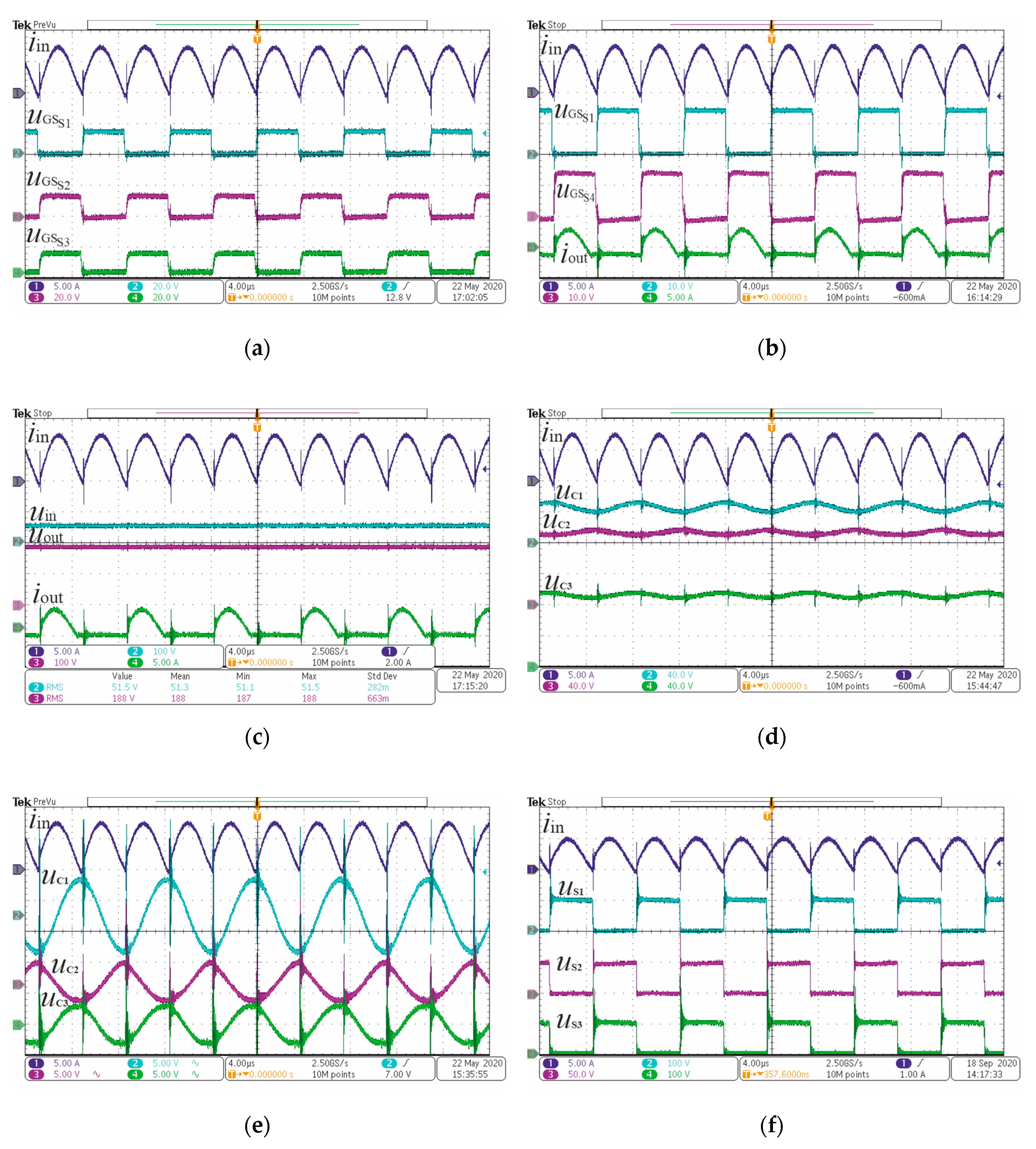
All the parameters of the converter used during the experimental research, as well as a photograph of the investigated converter, are collected in Table 5. The parameters of the experimental setup correspond to the simulation model, and the major difference can be found in the inductance of the planar PCB choke. The switching frequency in the experimental measurements has been adjusted to the oscillation period of the switched capacitor currents and differs from the value selected for the simulation tests. An IGBT switch was selected as S1 in the LSCVMb, as this switch conducts the total charging current. This current can be significant, especially when the converter contains a larger number of the switching cells. In order to generate appropriate control signals, an FPGA evaluation board (INTEL DE0) was utilized. The basic clock frequency of this device was set at 200 MHz, and the time resolution of the generated signals was 5 ns. The test setup is an example design of the converter prepared for the purpose of research, to verify its concepts and feasibility. The tests were conducted with 50 V at the input; however, the voltage range as well as power and the design concept can be rescaled to the parameters of a target application. Moreover, it is important that the prospective applications of the non-isolated DC-DC converter should comply with safety standards.

4.2. Test Results

Figure 13a,b presents the waveforms of the switching signals with the input and output current. They confirm that the converter operates correctly according to strategy C5. From the waveforms presented in Figure 13c, it follows that the converter boosts the input voltage. The measured voltage ratio is 3.65. Figure 13d,e presents the input current waveform and the voltages across the resonant capacitors. From the waveforms presented in Figure 13d, the average voltage across the capacitors can be seen. To demonstrate more clearly the magnitude of the oscillation around the average voltage value of each resonant capacitor, the voltage traces in AC coupling mode were recorded as well (Figure 13e). Figure 13f presents voltage stresses across the switches. From these results, it follows that the voltage stresses on switches are significantly below the output voltage of the converter, which is very favorable from the switching losses standpoint.
During the experimental research, the basic operation concept of the investigated converter has been checked. Furthermore, the working correctness of the examined device under different output loads was verified. The tests were carried out for three output load values: 62, 146, and 290 W, focusing especially on the transistor currents and voltages. Figure 14 present the results of the conducted tests for different output load conditions. From the results, it follows that the converter operates properly in low and medium load conditions.
Figure 15 presents the results of the spectral analysis calculated for the input and output currents. The calculations have been carried out with the use of MATLAB software, based on the recorded experimental data. The data was collected by the digital oscilloscope (Tektronix MDO3104) with the sampling rate of 1 MS/s.
The experimental results of the output voltage of the LCSCVMb converter and its efficiency are presented in Figure 16. The efficiency is on an acceptable level. The voltage and efficiency drop versus power is typical for such SC-based converters, and results from their resistive losses. It should be noticed that the presented experimental setup is optimized towards the converter cost reduction. It was designed on a two-layer PCB of 35 μm. To increase the efficiency by reducing the parasitic resistance, a more expensive PCB and switches can be selected.

5. Conclusions

The presented concepts of the new topologies, as well as the comparison of parameters presented in Table 3, and charts in Figure 8, Figure 9 and Figure 10, lead to the following conclusions:
  • The major idea of the proposed new converters is based on the elimination of the number of switches in a voltage multiplier (SCVM), while maintaining its proper operation. By the modification of an SCVM, the new topology concepts LCSCVMa and LCSCVMb were proposed, with a reduced number of switching cells and redesigned functions of the diodes. Depending on the technology of practical implementation, either of these converters can be more attractive than the other.
  • Various switching strategies are possible for the converters, which affect the parameters of operation related to switching losses and the sizing of the passive components of the converter, but also the required input and output filters.
  • The converter operates properly with a wide range of output loads.
  • From the compared results, it follows that the most effective topology, the LCSCVMb, can operate with nearly the lowest parameters of AC component in the voltages on capacitors, and the highest frequency in the input and output current. This allows for a reduction of the converter volume, especially by optimizing the input and output filters.
  • The discussed converters demonstrated an improvement in the SCVM topology, which may result in a prospective cost reduction.

Author Contributions

Conceptualization, R.S.; methodology, R.S. and Z.W.; software, R.S., Z.W. and S.F.; validation, R.S., Z.W. and S.F.; formal analysis, R.S. and Z.W.; investigation, R.S., Z.W. and S.F.; resources, R.S.; data curation, R.S., Z.W. and S.F.; writing—original draft preparation, R.S., Z.W. and S.F.; writing—review and editing, visualization, supervision, R.S., Z.W. and S.F.; project administration, R.S. All authors have read and agreed to the published version of the manuscript.

Funding

This research received no external funding.

Conflicts of Interest

The authors declare no conflict of interest.

References

  1. Ioinovici, A. Switched-capacitor power electronics circuit. IEEE Circuits Syst. Mag. 2001, 1, 37–42. [Google Scholar] [CrossRef]
  2. Tofoli, F.L.; de Castro Pereira, D.; de Paula, W.J.; Júnior, D.S.O. Survey on non-isolated high-voltage step-up dc–dc topologies based on the boost converter. IET Power Electron. 2015, 8, 2044–2057. [Google Scholar] [CrossRef] [Green Version]
  3. Forouzesh, M.; Siwakoti, Y.P.; Gorji, S.A.; Blaabjerg, F.; Lehman, B. Step-Up DC–DC Converters: A Comprehensive Review of Voltage-Boosting Techniques, Topologies, and Applications. IEEE Trans. Power Electron. 2017, 32, 9143–9178. [Google Scholar] [CrossRef]
  4. Wu, G.; Ruan, X.; Ye, Z. Nonisolated High Step-Up DC–DC Converters Adopting Switched-Capacitor Cell. IEEE Trans. Ind. Electron. 2015, 62, 383–393. [Google Scholar] [CrossRef]
  5. Li, W.; He, X. Review of Nonisolated High-Step-Up DC/DC Converters in Photovoltaic Grid-Connected Applications. IEEE Trans. Ind. Electron. 2011, 58, 1239–1250. [Google Scholar] [CrossRef]
  6. Raghavendra, K.V.G.; Zeb, K.; Muthusamy, A.; Krishna, T.N.V.; Kumar, S.V.S.V.P.; Kim, D.-H.; Kim, M.-S.; Cho, H.-G.; Kim, H.-J. A Comprehensive Review of DC–DC Converter Topologies and Modulation Strategies with Recent Advances in Solar Photovoltaic Systems. Electronics 2020, 9, 31. [Google Scholar] [CrossRef] [Green Version]
  7. Liu, W.; Niazi, K.A.K.; Kerekes, T.; Yang, Y. A Review on Transformerless Step-Up Single-Phase Inverters with Different DC-Link Voltage for Photovoltaic Applications. Energies 2019, 12, 3626. [Google Scholar] [CrossRef] [Green Version]
  8. Xiao, H. Overview of Transformerless Photovoltaic Grid-Connected Inverters. IEEE Trans. Power Electron. 2020, 36, 533–548. [Google Scholar] [CrossRef]
  9. Alluhaybi, K.; Batarseh, I.; Hu, H. Comprehensive Review and Comparison of Single-Phase Grid-Tied Photovoltaic Microinverters. IEEE J. Emerg. Sel. Top. Power Electron. 2020, 8, 1310–1329. [Google Scholar] [CrossRef]
  10. Tran, V.-T.; Nguyen, M.-K.; Choi, Y.-O.; Cho, G.-B. Switched-Capacitor-Based High Boost DC-DC Converter. Energies 2018, 11, 987. [Google Scholar] [CrossRef] [Green Version]
  11. Lee, J.; Jeong, Y.; Han, B. An Isolated DC/DC Converter Using High-Frequency Unregulated LLC Resonant Converter for Fuel Cell Applications. IEEE Trans. Ind. Electron. 2011, 58, 2926–2934. [Google Scholar] [CrossRef]
  12. Cao, D.; Peng, F.Z. A family of zero current switching switched-capacitor dc-dc converters. In Proceedings of the 2010 25th Annual IEEE Applied Power Electronics Conference and Exposition (APEC), Palm Springs, CA, USA, 21–25 February 2010; pp. 1365–1372. [Google Scholar]
  13. Waradzyn, Z.; Stala, R.; Mondzik, A.; Penczek, A.; Skala, A.; Pirog, S. Efficiency analysis of MOSFET-based air-choke resonant DC–DC step-up switched-capacitor voltage multipliers. IEEE Trans. Ind. Electron. 2017, 64, 8728–8738. [Google Scholar] [CrossRef]
  14. Penczek, A.; Mondzik, A.; Waradzyn, Z.; Stala, R.; Skała, A.; Piróg, S. Switching strategies of a resonant switched-capacitor voltage multiplier. In Proceedings of the 2017 19th European Conference on Power Electronics and Applications (EPE’ 17 ECCE Europe), Warsaw, Poland, 11–14 September 2017; pp. 1–10. [Google Scholar]
  15. Xie, W.; Li, S.; Zheng, Y.; Smedley, K.; Wang, J.; Ji, Y.; Yu, J. A Step-up Series-parallel Resonant Switched-capacitor Converter with Extended Line Regulation Range. In Proceedings of the 2019 IEEE Applied Power Electronics Conference and Exposition (APEC), Anaheim, CA, USA, 17–21 March 2019; pp. 2150–2154. [Google Scholar]
  16. Stala, R.; Waradzyn, Z.; Mondzik, A.; Penczek, A.; Skała, A. DC–DC High Step-up Converter with Low Count of Switches Based on Resonant Switched-Capacitor Topology. In Proceedings of the 2019 21st European Conference on Power Electronics and Applications (EPE’ 19 ECCE Europe), Genova, Italy, 3–5 September 2019; pp. 1–10. [Google Scholar]
  17. Xie, H.; Li, R. A Novel Switched-Capacitor Converter with High Voltage Gain. IEEE Access 2019, 7, 107831–107844. [Google Scholar] [CrossRef]
  18. Lei, H.; Hao, R.; You, X.; Li, F. Nonisolated High Step-Up Soft-Switching DC–DC Converter with Interleaving and Dickson Switched-Capacitor Techniques. IEEE J. Emerg. Sel. Top. Power Electron. 2020, 8, 2007–2021. [Google Scholar] [CrossRef]
  19. He, L.; Zheng, Z. High step-up DC–DC converter with switched-capacitor and its zero-voltage switching realization. IET Power Electron. 2017, 10, 630–636. [Google Scholar] [CrossRef]
  20. Chen, M.; Li, K.; Hu, J.; Ioinovici, A. Generation of a Family of Very High DC Gain Power Electronics Circuits Based on Switched-Capacitor-Inductor Cells Starting from a Simple Grap. IEEE Trans. Circuits Syst. 2016, 63, 2381–2392. [Google Scholar] [CrossRef]
  21. Kawa, A.; Stala, R. A multilevel switched capacitor DC–DC converter. An analysis of resonant operation conditions. Power Electron. Drives 2016, 1, 35–53. [Google Scholar]
  22. Kawa, A.; Stala, R. SiC-Based Bidirectional Multilevel High-Voltage Gain Switched-Capacitor Resonant Converter with Improved Efficiency. Energies 2020, 13, 2445. [Google Scholar] [CrossRef]
  23. Li, S.; Zheng, Y.; Wu, B.; Smedley, K.M. A Family of Resonant Two-Switch Boosting Switched-Capacitor Converter with ZVS Operation and a Wide Line Regulation Range. IEEE Trans. Power Electron. 2018, 33, 448–459. [Google Scholar] [CrossRef]
  24. Qian, W.; Cao, D.; Cintron-Rivera, J.G.; Gebben, M.; Wey, D.; Peng, F.Z. A Switched-Capacitor DC–DC Converter with High Voltage Gain and Reduced Component Rating and Count. IEEE Trans. Ind. Appl. 2012, 48, 1397–1406. [Google Scholar] [CrossRef]
  25. Xiong, S.; Tan, S. Cascaded High-Voltage-Gain Bidirectional Switched-Capacitor DC–DC Converters for Distributed Energy Resources Applications. IEEE Trans. Power Electron. 2017, 32, 1220–1231. [Google Scholar] [CrossRef]
  26. Stala, R.; Piróg, S. DC–DC boost converter with high voltage gain and a low number of switches in multisection switched capacitor topology. Arch. Electr. Eng. 2018, 67, 617–627. [Google Scholar]
  27. Kumar, A.; Wang, Y.; Pan, X.; Raghuram, M.; Singh, S.K.; Xiong, X.; Tripathi, A.K. Switched-LC Based High Gain Converter with Lower Component Count. IEEE Trans. Ind. Appl. 2020, 56, 2816–2827. [Google Scholar] [CrossRef]
  28. Li, S.; Smedley, K.M.; Caldas, D.R.; Martins, Y.W. Hybrid Bidirectional DC–DC Converter with Low Component Counts. IEEE Trans. Ind. Appl. 2018, 54, 1573–1582. [Google Scholar] [CrossRef]
  29. Waradzyn, Z.; Stala, R.; Skała, A.; Mondzik, A.; Penczek, A. A cost-effective resonant switched-capacitor dc-dc boost converter—Experimental results and feasibility model. Power Electron. Drives 2018, 3, 75–83. [Google Scholar] [CrossRef] [Green Version]
  30. Wu, G.; Ruan, X.; Ye, Z. High Step-Up DC–DC Converter Based on Switched Capacitor and Coupled Inductor. IEEE Trans. Ind. Electron. 2018, 65, 5572–5579. [Google Scholar] [CrossRef]
  31. Kazimierczuk, M.K.; Czarkowski, D. Resonant Power Converters, 2nd ed.; Wiley: Hoboken, NJ, USA, 2011. [Google Scholar]
Figure 1. Proposed new resonant converters with low count of switches and common input/output negative point: (a) LCSCVMa, (b) LCSCVMb.
Energies 13 05657 g001
Figure 2. Steady-state operation of the LCSCVMa converter under switching strategy C1: (a) waveforms of the gate to source signals of transistors (presented with level shift), input current (in amperes), and voltages (in volts) on capacitors C1, C2, and C3. (b) Spectrum of the input current, and currents of switched capacitors and output capacitor. The results were obtained with the use of ICAP/4 simulation software.
Energies 13 05657 g002
Figure 3. Steady-state output current and voltage waveforms of the LCSCVMb converter under switching strategy C1 (4 A/div and 100 mV/div). The results were obtained with the use of ICAP/4 simulation software.
Energies 13 05657 g003
Figure 4. Steady-state operation of the LCSCVMa converter under switching strategy C2: (a) waveforms of the gate to source signals of transistors (presented with level shift), input current (in amperes), and voltages (in volts) on capacitors C1, C2, and C3. (b) Spectrum of the input current, and currents of switched capacitors and output capacitor. The results were obtained with the use of ICAP/4 simulation software.
Energies 13 05657 g004
Figure 5. Steady-state operation of the LCSCVMa converter under switching strategy C3: (a) waveforms of the gate to source signals of transistors (presented with level shift), input current (in amperes), and voltages (in volts) on capacitors C1, C2, and C3. (b) Spectrum of the input current, and currents of switched capacitors and output capacitor. The results were obtained with the use of ICAP/4 simulation software.
Energies 13 05657 g005
Figure 6. Steady-state operation of the LCSCVMb converter under switching strategy C4: (a) Waveforms of the input current, inductor currents, and the current of the output diode (in amperes). (b) Voltages (in volts) on capacitors C1, C2, and C3. The results were obtained with the use of ICAP/4 simulation software.
Energies 13 05657 g006
Figure 7. Steady-state operation of the LCSCVMb converter under switching strategy C5: (a) Waveforms of the input current, inductors currents, and the current of the output diode (in amperes). (b) Voltages (in volts) on capacitors C1, C2, and C3. The results were obtained with the use of ICAP/4 simulation software.
Energies 13 05657 g007
Figure 8. Comparison of converters’ parameters under strategies C1–C5: Ratios of number of switches (axis 1) and number of diodes (axis 2) to those in SCVM (on the basis of data in Table 3). Quantity proportional to undesired output voltage decrease: 0.06·(200 – Uout) (axis 3). Ratios of the lowest frequencies in the input and output current: 0.4·fac_in SCVM/fac_in (axis 4), 0.4·fac_out SCVM/fac_out (axis 5).
Energies 13 05657 g008
Figure 9. Ratios of the following parameters of strategies C1–C5 (axes 1–5): (a) Peak-to-peak voltages across capacitors C1C3, (b) rms and maximum values of currents in inductances L1L3. The results are based on the data in Table 3.
Energies 13 05657 g009
Figure 10. Ratios of the following parameters (strategies C1–C5) to the corresponding parameter of SCVM: (a) Peak-to-peak voltages across capacitors C1C3, (b) rms (axes 1–3) and maximum values of currents in inductances L1L3 (axes 4–6). The results are based on the data in Table 3.
Energies 13 05657 g010
Figure 11. Current paths in the LCSCVMa: (a) in the stage 1 and (b) in the stage 2.
Energies 13 05657 g011
Figure 12. Theoretical charts of efficiency vs. fSn = fS/f0 for three values of rn: 0.016, 0.0304, and 0.040, and ΔUDn = 0.008: (a) LCSCVMa at switching losses ΔPsw0n = 0.0138, (b) LCSCVMb at switching losses ΔPsw0n = 0.0101.
Energies 13 05657 g012
Figure 13. A set of recorded waveforms during experimental tests: (a) Switching signals of transistors and the input current, (b) input and output current of the converter on the background of switching signals, (c) input and output waveforms of the converter (current and voltage traces), (d) converter input current and voltages across resonant capacitors recorded in DC coupling mode, (e) converter input current and voltages across resonant capacitors recorded in AC coupling mode, and (f) voltage stresses across the switches on the background of converter input current. Switching strategy C5.
Energies 13 05657 g013
Figure 14. Waveforms of the input current as well as the currents and voltages across switches, during experimental test proceeded with different values of converter output power: (ac) Pout = 62 W, 2A/div, 100V/div, (df) Pout = 146 W, 5A/div, 100V/div, (gi) Pout = 290 W, 10A/div, 100V/div. Switching strategy C5.
Energies 13 05657 g014
Figure 15. Results of spectral analysis for: (a) The input current and (b) the output current.
Energies 13 05657 g015
Figure 16. Experimental and simulation results for LSSCVMb under strategy C5 at Uin = 50 V, fS = 133 kHz: (a) Measured output voltage Uout vs. Pout, (b) measured efficiency vs. Pout with comparison to theoretical results obtained from (34) for r = 380 mΩ, VF = 400 mV, VCE(on) = 1 V, Wsw = 11 μJ.
Energies 13 05657 g016
Table 1. Switching strategy concepts of the LCSCVMa. States of switches S1S4.
The Concept for Switching Strategy of LCSCVMaDescription—Stages of Charge Transfer in the Converter
Strategy C1 Energies 13 05657 i0011.Simultaneous charging of all the switched capacitors
2. Discharging of the capacitor that is the nearest to the source (C1) to the internal branch (C2)
3. Charging C1, and discharging C2 and the next SC capacitor (C3) to the output
4. Discharging C1 to the internal branch (as in 2)
5. Discharging C2 and C3 to the output
Strategy C2 Energies 13 05657 i0021. Simultaneous charging of all the switched capacitors
2. Discharging C1 to the internal branch (C2)
3. Discharging C2 and C3 to the output
Strategy C3 Energies 13 05657 i0031. Simultaneous charging of all the switched capacitors (C1 and C3)
2. Simultaneous discharging of all the switched capacitors and charging the internal branch capacitor (C2)
Table 2. Switching strategy concepts of the LCSCVMb. States of switches S1, S2, and S4.
The Concept for Switching Strategy of LCSCVMbDescription—Stages of Charge Transfer in the Converter
Strategy C4 Energies 13 05657 i004Similarly to strategy C2 for the LCSCVMa, strategy C4 gives the following characteristic in the LCSCVMb:
1. Simultaneous charging of all the switched capacitors
2. Discharging C1 to the internal branch (C2)
3. Discharging C2 and C3 to the output
Strategy C5 Energies 13 05657 i005Similarly to strategy C3 for the LCSCVMa, strategy C5 gives the following characteristic in the LCSCVMb:
1. Simultaneous charging of all the switched capacitors
2. Simultaneous discharging of all the switched capacitors and charging the internal branch (C2)
Table 3. Major parameters comparison among the parameters of LCSCVMa and LCSCVMb converters in the tests of 200 W operation.
Parameter LCSCVMa Strategy LCSCVMb Strategy SCVM
C1 C2 C3 C4 C5
No. of switches444336
No. of diodes444554
Uout, V178.0177.0185.0172.1181.4191.2
TS, μs21.012.68.412.68.48.4
fac_in, kHz47.679.4238.179.4238.1238.1
fac_out, kHz47.679.4119.079.4119.0119.0
UC1p-p, V21.0219.4112.419.812.65.98
UC2p-p, V21.6119.416.5419.86.655.98
UC3p-p, V16.089.76.189.926.295.98
IL1_rms, A6.757.255.657.415.752.73
IL2_rms, A6.226.282.926.422.972.73
IL3_rms, A4.113.632.753.712.802.73
IL1_max, A16.114.89.4615.19.604.57
IL2_ max, A13.214.85.0115.25.094.57
IL3_ max, A12.37.434.747.564.804.57
Symmetry of current iL1noyesyesyesyesyes
Symmetry of current iL2nonoyesnoyesyes
Symmetry of current iL3noyesyesyesyesyes
Table 4. Comparison of the number of switches and diodes, and the lowest frequency of the input current in selected topologies versus the voltage gain. Ref. = Reference.
ParameterToplogy
GainLCSCVMaLCSCVMbRef. [13]Ref. [22]Ref. [16]Ref. [25]Ref. [26]Ref. [27]
No. of switches(and diodes)44 (4)3 (5)6 (4)8 (0)-8 (0)4 (4)4 (6)
7--12 (7)14 (0)7 (5)--7 (12)
86 (6)4 (7)14 (8)16 (0)-12 (0)6 (6)8 (14)
fiin_min/fSmax for all gains(fSmax—in (1))110.511/4110.5
Table 5. The most important parameters of the laboratory converter.
ParameterValueThe Laboratory Setup
Input voltage50 V Energies 13 05657 i006
Output load200 W
Switching frequency133 kHz
Resonant capacitors1.5 µF (KEMET R76 series)
Resonant inductancesPlanar chokes: L = 500 nH, RESR = 18 mΩ @ 100 kHz
TransistorsIKB15N65EH5 (VDS = 650 V, VCE = 1.65 V) as S1
IPB50R140CP (VDS = 550 V, RDSon = 0.14 Ω) as S2 and S4
DiodesSTTH30L06G (IF = 30 A, VF = 1.0 V, VRRM = 600 V)
PCB2 layers, 35 µm
Laboratory equipmentDigital scope: Tektronix MDO3104, current probes: Tektronix TCP0030 150 MHz (input current measurement), Rogowsky coil (switch current measurements) voltage probes: Tektronix THDP0200 200 MHz, Tektronix P5205 100 MHz, power analyzer: Yokogawa WT 1801
Publisher’s Note: MDPI stays neutral with regard to jurisdictional claims in published maps and institutional affiliations.

