Article

Phototransistor Behavior in CIGS Solar Cells and the Effect of the Back Contact Barrier

1
Instituto de Energía Solar—ETSIT, Universidad Politécnica de Madrid, Avenida Complutense 30, 28040 Madrid, Spain
2
Institute of Mechatronics and Medical Engineering, Ulm University of Applied Sciences, Albert-Einstein-Allee 55, 89081 Ulm, Germany
3
Zentrum für Sonnenenergie und Wasserstoff, Meitnerstr. 1, 70563 Stuttgart, Germany
4
Nice Solar Energy GmbH, Alfred-Leikam-Str. 25, 74523 Schwäbisch Hall, Germany
*
Author to whom correspondence should be addressed.
Energies 2020, 13(18), 4753; https://doi.org/10.3390/en13184753
Submission received: 12 August 2020 / Revised: 4 September 2020 / Accepted: 9 September 2020 / Published: 11 September 2020
(This article belongs to the Special Issue Recent Advances in Thin Film Solar Cells)

Abstract

:
In this paper, the impact of the back contact barrier on the performance of Cu (In, Ga) Se2 solar cells is addressed. This effect is clearly visible at lower temperatures, but it also influences the fundamental parameters of a solar cell, such as open-circuit voltage, fill factor and the efficiency at normal operation conditions. A phototransistor model was proposed in previous works and could satisfactorily explain specific effects associated with the back contact barrier, such as the dependence of the saturated current in the forward bias on the illumination level. The effect of this contribution is also studied in this research in the context of metastable parameter drift, typical for Cu (In, Ga) Se2 thin-film solar cells, as a consequence of different bias or light soaking treatments under high-temperature conditions. The impact of the back contact barrier on Cu (In, Ga) Se2 thin-film solar cells is analyzed based on experimental measurements as well as numerical simulations with Technology Computer-Aided Design (TCAD). A barrier-lowering model for the molybdenum/Cu (In, Ga) Se2 Schottky interface was proposed to reach a better agreement between the simulations and the experimental results. Thus, in this work, the phototransistor behavior is discussed further in the context of metastabilities supported by numerical simulations.

Graphical Abstract

1. Introduction

The exponential increase in the demand of green energy is one of the environmental challenges which are currently faced in the energy sector. One of the most reliable sources of green energy is the generation of electricity from the sun, a field in which different technologies compete for the lowest energy production cost. Cu (In, Ga) Se2 (CIGS)-based thin-film solar cells are one of the most promising technologies due to their rapid efficiency improvement. Some of the latest breakthroughs, such as the record efficiency over 23% achieved in a laboratory [1] or an 18% efficiency on a large area module [2], put this material at the same level as crystalline silicon devices in terms of photovoltaic potential.
The attractiveness of CIGS as a thin-film technology can be explained by the small amount of materials required to produce a solar panel, because the thickness of the device layers is typically in the range of a few microns. The layers that are normally present in thin-film solar cells are as follows: (i) a transparent front contact (TCO), which in CIGS devices is usually an n-type doped zinc oxide (ZnO) film of around 0.3 µm [3], although other alternatives are possible; (ii) a buffer layer as an interface between the front contact and the absorber—in CIGS, a thin cadmium sulfide (CdS) layer of 20 to 50 nm is used [4], although there is ongoing research to replace this toxic material with a more environmentally friendly one [1,5,6]; (iii) the absorber, in this case, is a Cu (In, Ga) (S, Se)2 compound semiconductor with a thickness between 1–3 µm, and in some cases even lower thicknesses are reported, such as in [7,8]; (iv) the absorber is deposited on top of the back contact, which is usually a molybdenum (Mo) layer of 0.2 to 1 µm [9]; (v) all these materials are deposited on a soda-lime glass substrate that supplies sodium (Na) to the sample to enhance its performance [10,11]. However, excess Na was reported to degrade the performance of the solar cell [12]. Na was also found to play an important role in the degradation of CIGS solar cells when exposed to detrimental operation conditions, such as high temperatures, high humidity or externally applied biases, which lead to one of the most damaging mechanisms for CIGS solar cells, referred to as potential-induced degradation (PID) [13,14].
Improving CIGS solar cells over the current efficiency record requires a better understanding of loss mechanisms and the underlying physical principles [15]. A barrier at the back contact interface (Mo/CIGS) is known to be a potential loss mechanism due to the formation of a second junction, but with opposite polarity. The effect of this barrier can be seen in low-temperature current–voltage (I–V) measurements as blocking behavior of the current under forward bias, also named as the roll-over effect [16,17,18,19,20]. Moreover, it affects other parameters of the solar cell, such as the fill factor and the open-circuit voltage (Voc) of the device, and thereby, the efficiency. Other barriers, induced by bandgap gradients or a band offset at the CIGS/CdS interface, are a plausible source of performance losses in CIGS solar cells, although they typically present their own unique signatures in low-temperature I–V measurements, such as the S-kink [21,22] or a complete blocking of the current under forward bias [23].
The impact of these barriers on the electronic transport can be diminished or enhanced in CIGS solar cells as a consequence of a metastable behavior that is typical for this technology. In [24], for instance, CIGS samples with different buffer layers are treated with light soaking and reverse bias at room temperature. The results of [24] show that a reverse-bias treatment induces a distortion, or roll-over, of the I–V curve that is more pronounced at low temperatures, where the metastable changes are not reversible. When the samples were left to relax at room temperatures, the distortion of the I–V curve was not found. The barrier was correlated in [24] with the N1 defect that is found in CIGS solar cells with admittance spectroscopy as a step in the capacitance–frequency curve.
The fill factor of the cell is also affected depending on the treatment; for instance, in [25,26] a reverse-bias treatment was found to induce a shunt in the I–V curve that resembles the S-kink previously mentioned. At low temperatures of 120 K, this metastable behavior is frozen, which means that it does not relax to the initial state. Light soaking, on the other hand, increases the fill factor and decreases the shunts in the I–V curves [25]. These two effects are correlated in [26,27] with redistributions of charges in the absorber; the reverse-bias treatment, for instance is suggested to enhance an already existing barrier in the form of a p+ -type “defected” layer that is found at the ZnO/CdS/CIGS heterointerface on the absorber’s side. Light soaking and forward-bias treatments reduce the amount of accumulated charges in this layer according to [25,28]. Both treatments are also known to increase the apparent carrier concentration that is found in capacitance–voltage (C–V) measurements calculated from the Mott–Schottky equation [28]. Redistribution of charges is explained in [26] and [29] as a change of the configuration of VSe–VCu complexes. Reverse-bias treatments, for instance, convert those complexes near the heterointerface from the donor into the acceptor configuration, while in the bulk, the opposite happens. With light soaking and forward bias [29], the situation is reversed. These changes could explain the variations in the net-doping level extracted from the C–V profile using the Mott–Schottky equation, and the shunts induced in the I–V curve by means of the p+ type “defect” layer previously mentioned. However, the effects of the changes induced by these treatments should also be considered regarding the Schottky back contact interface, as in [30].
The origin of the Schottky barrier is still up for debate because of the existence of a thin MoSe2 layer between the Mo/CIGS layers. Although the Mo/MoSe2 interface behaves as a Schottky barrier for holes, the Mo/CIGS junction is quasi-ohmic when a thin MoSe2 layer exists [17]. The thickness and other physical properties of this thin MoSe2 layer depend primarily on the fabrication process. In [17], two deposition processes for CIGS are compared, namely the two-step selenization after sulfurization (SAS), and the sequential sputtering/selenization process [31]. The latter process was found in [17] to create no MoSe2, and a Schottky barrier appeared at the Mo/CIGS interface reducing the performance of the cell. In the SAS process, on the other hand, a thin MoSe2 layer was formed according to [17], and the negative effect of the barrier on the performance was diminished.
The simplest model that considers this blocking behavior at low temperatures in thin-film solar cells is based on the five-parameter model [32], which includes an additional diode with a polarity that opposes that of the pn junction [33]. Notwithstanding, this model with two opposing diodes presents some limitations, such as its inability to reproduce the dependence of the saturated forward current on the illumination level, a side effect of the back contact barrier that is also visible in experimental results. A phototransistor model was proposed in [19,34,35] to account for this effect; in this model, the solar cell is presented in a similar manner as an npn bipolar phototransistor, in which the absorber is the equivalent of the (very thick) base, while ZnO/CdS represents the emitter, and Mo is the collector. With a forward bias applied to the solar cell, the ZnO/CdS/CIGS pn junction is polarized in the forward direction, while the Mo/CIGS junction is polarized in the reverse direction, which means that the photogenerated carriers are separated by the latter junction. The current extracted in the forward bias is modulated by the illumination level, and the relation between both is represented by a gain factor in the same manner as in a normal transistor [34].
Other issues related to the phototransistor model can be also seen in the I–V curves of CIGS solar cells, such as the Early effect or the punch-through effect. The first consists of a linear increase in the emitter–collector current when the bias between both terminals increases, instead of a perfect saturation because of the proximity between both space charge regions (SCR) that reduces the carrier recombination. It can be found in the I–V curves of CIGS solar cells under certain conditions, for instance, in very thin absorbers or in a low-doping absorber concentration [36]. The punch-through is the extreme case of the Early effect; when both SCRs overlap, the current increases exponentially with the applied bias, and a significant decrease in Voc is also found in solar cells when this effect takes place under normal conditions [37]. The punch (or reach)-through effect was first reported in cadmium telluride (CdTe) solar cells [38] but is also known to occur in CIGS devices [37].
The phototransistor effect is mostly visible in the I–V curves measured at low temperatures in the range from 100 to 200 K. However, it was also reported that accelerated ageing tests might induce this effect even at room temperature [30] because of the oxidation of the Mo back contact, and a decrease in the apparent doping due to the metastable redistribution of charges that was previously mentioned. According to [39], this decrease in doping level is responsible for an increase in non-radiative recombination at the heterointerface on the absorbers side.
This article discusses the effect of the back contact barrier on the performance of CIGS solar cells from the perspective of the phototransistor model introduced in [34]. The results hereby presented provide strong evidence in support of this phototransistor model. Moreover, the effect of the back contact barrier is considered in the broader context of metastable changes typical for CIGS solar cells, induced by certain operation conditions dependent on the temperatures or electrical biases. The gain factor in the phototransistor model was also found to be affected depending on the applied treatment, and, in some cases, the treatment could induce the phototransistor behavior even at high temperatures (350 K). A barrier-lowering effect was proposed for the simulation model presented in this paper to explain a slight exponential increase in the current under forward bias that appears in the experimental I–V measurements on some of the samples. The punch-through effect is described in this paper as a side effect of the phototransistor model that could influence the performance of CIGS solar cells detrimentally, especially in very thin absorbers where the SCRs of both junctions are very close each other.
In summary, the effect of the back contact barrier on the phototransistor behavior was discussed in detail in this contribution. Furthermore, a relation between metastabilities and the phototransistor effect is established and supported by numerical modelling. Finally, barrier lowering as a consequence of high electric fields is proposed within the phototransistor model in order to account for experimental findings.
The article is divided into five parts. The introduction provides the reader with a concise context of the paper and a comprehensive literature review of the topic. The third chapter describes the results and is divided into two sections. The first section demonstrates the experimental results obtained from the characterization of CIGS solar cells, in particular the I–V curves of samples that were treated under different operation conditions (high temperatures and electrical biases), and other parameters extracted from the aforementioned samples, such as activation energies and barrier heights. The second section of part three discusses the I–V curves obtained from the simulation cases corresponding to the experiments, and also provides the calculated values of the activation energies and barrier heights mentioned above; the effect of the barrier-lowering in the model and the punch-through effect are also discussed with respect to the corresponding I–V curves. The fourth part discusses the results presented in chapter three in the framework of the phototransistor model. Finally, the conclusions summarize the findings of this paper and discuss the applications and research questions that are still open.

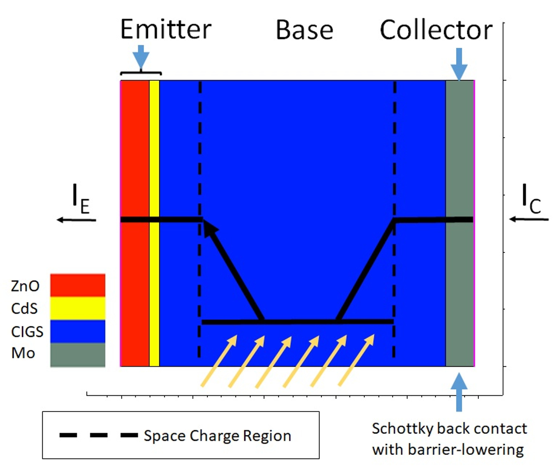
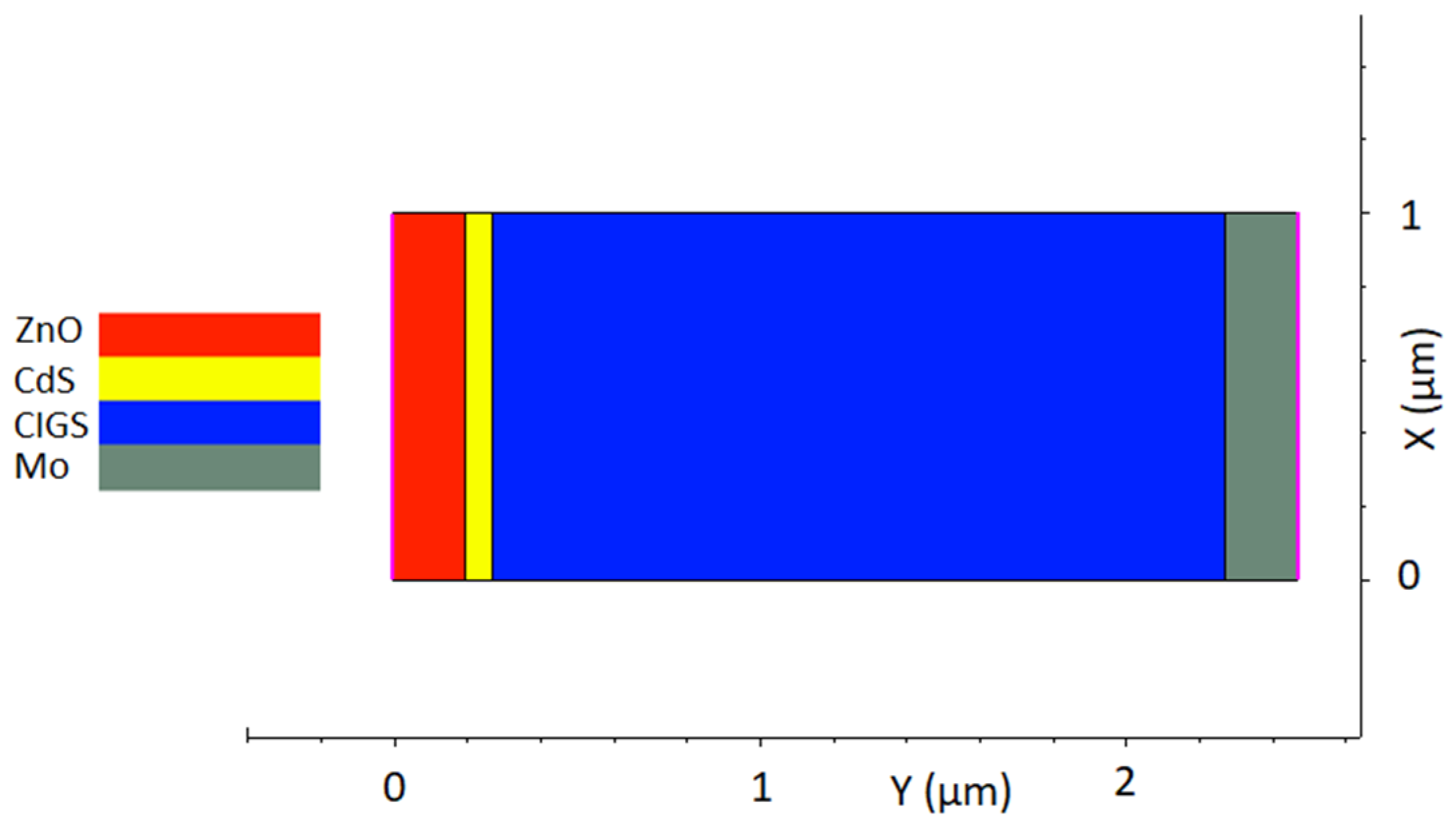
2. Materials and Methods
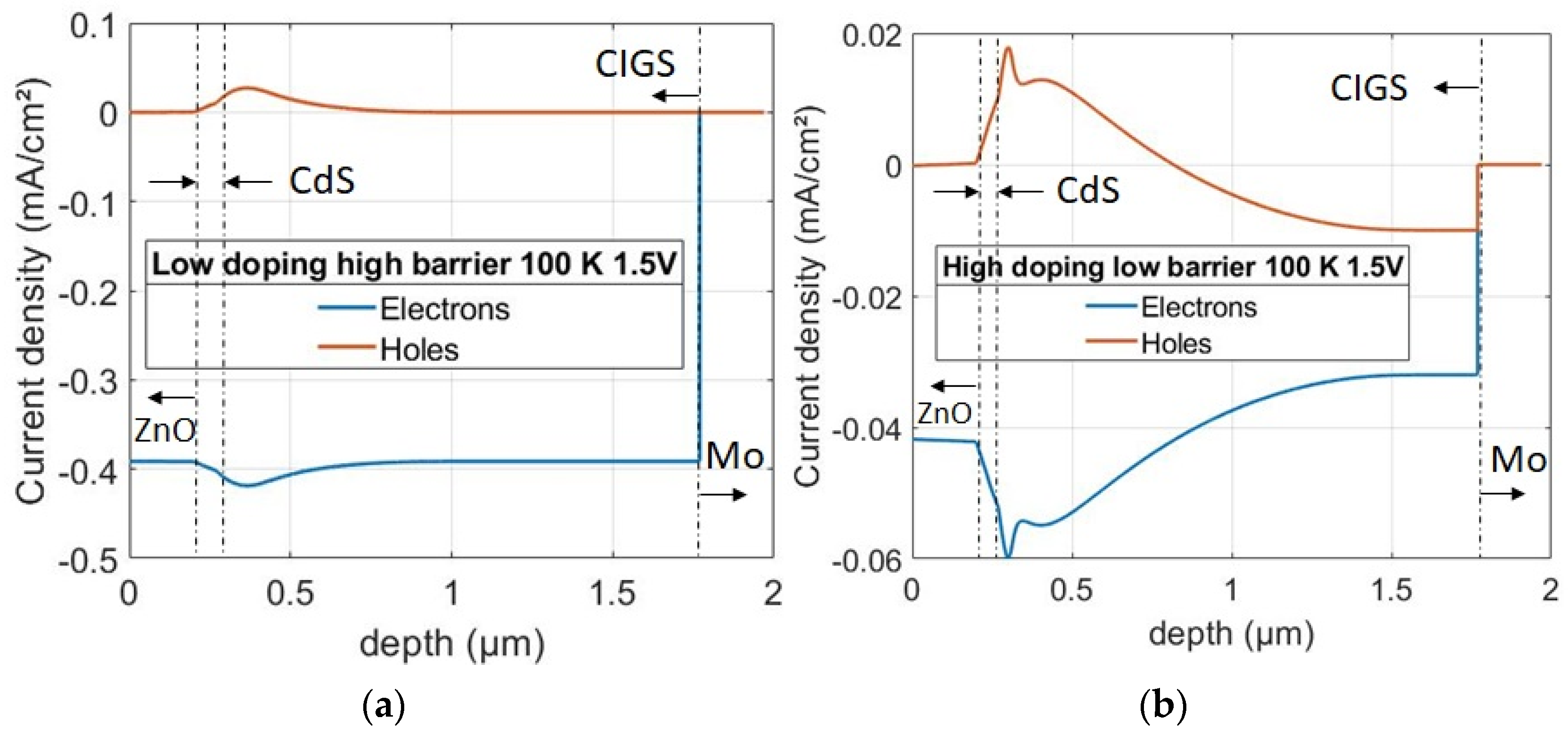
Both numerical simulations and experimental characterization were used in the development of this work, and their findings are in good agreement.
All the experimental results involve the electrical characterization of the samples in a wide range of temperatures, mainly because the phototransistor behavior is visible only in low-temperature regimes. From temperature-dependent current–voltage (I–V) characterization, it is possible to extract the activation energy and the height of the potential barrier at the back contact [40]. Both parameters are calculated from the extrapolation of the Voc (T) values to 0 K in the low- and high-temperature regimes, as the results will show.
Three CIGS samples from the same batch grown by a three-stage co-evaporation process, with similar behavior of the I–V curves, were characterized in this work. An accelerated ageing test consisting of a high temperature treatment and different biases was applied to two of the samples (+0.4 V to one of the treated samples and −0.4 V to the other) over a period of 16 h at 100 °C to assess how these detrimental conditions alter the effect of the back contact barrier and the phototransistor behavior. These treatments were performed by placing two of the samples in a WKL 34/40 climate chamber [41] (Weiss Umwelttechnik, Stuttgart, Germany) with an external connection to a Keithley 4200-SCS Semiconductor Analyzer [42] (Tektronix, Beaverton, OR, USA) that was applied to the sample the appropriate bias and monitored the I–V curve every hour. The third sample was only kept at room temperature.
After these treatments, each sample was characterized in the temperature range from 100 K to 400 K in steps of 25 K. This was achieved by placing the samples in an OptistatDN-V model cryostat (Oxford Instruments-Nanoscience [43], Oxford, UK) cooled with liquid nitrogen. The cryostat includes an external connector to perform the electrical measurements. The I–V curves were measured with a 4155 C Semiconductor Analyzer [44] (Keysight, Santa Rosa, CA, USA). The cryostat also has a small glass aperture in the measurement chamber to illuminate the sample when needed. In this case, the external illumination for light I–V measurements was provided by a LOT-Oriel LSE 340 solar simulator (Quantum Design GmbH, Darmstadt, Germany), and a set of transmission filters was used to regulate the illumination level. The effective doping concentration was calculated based on the Mott–Schottky equation [28] from the capacitance–voltage profiles measured at 300 K with 4192 LF Impedance Analyzer [45] (Keysight, Santa Rosa, CA, USA) with a frequency and magnitude of alternating current (AC) signal of 100 kHz and 50 mV, respectively. A parallel circuit model consisting of a resistor and a capacitor was selected in the instrument for the extraction of the capacitance from the solar cell.
The simulations were performed by means of the Sentaurus TCAD suite [46] (Synopsys, Palo Alto, CA, USA). The simulation model consists of a vertical stack of ZnO/CdS/CIGS/Mo, each material with the properties presented in Table 1, including the physical dimensions of each layer, doping levels, bandgap energies and electron affinities where appropriate and other parameters that are relevant for the simulations in the scope of this work.
Apart from these layers, the Mo/CIGS interface is defined as a Schottky interface with a barrier that is adjusted through the work function of Mo and a surface recombination velocity of 1 × 107 cm2/s for electrons and holes. The interface model also includes a barrier-lowering effect [36] to represent another minor effect found in the experimental results presented in this work. In this model, the height of the barrier decreases when the component of the electric field that is perpendicular to the Mo/CIGS interface increases. Barrier lowering is a known property of Schottky barriers that could be attributed to tunneling or to a force exerted by image charges at the Mo/CIGS interface according to [36]. The equation in [36] that describes the barrier-lowering mechanism is presented in Equation (1).
Δ Φ B = q · E n o r m 4 · π · ε s
In this equation, ∆ΦB is the barrier lowering in eV, q is the elementary electric charge, Enorm is the component of the electric field that is normal to the metal–semiconductor interface and εs is the dielectric permittivity of CIGS at the Mo/CIGS interface; a value of 10 was selected for the relative permittivity of CIGS. However, when tunneling is considered instead, the equation might be slightly different. In the presented simulations, the empirical model provided by Synopsys TCAD was used. This model includes a multiplicative factor of 2.2 × 10⁻⁴ eV and an exponential factor of 0.5, both of which are applied to the component of the electric field that is normal to the Mo/CIGS interface.
The model of the solar cell stack used for the simulation is presented in Figure 1 with a horizontal orientation and an absorber thickness of 2.0 µm. Simulations are performed in the range of temperatures between 100 K to 400 K with steps of 50 K.
Finally, the punch-through effect that was mentioned in the introduction will be discussed in the context of simulations by adjusting the thickness of the absorber and its doping concentration in order to increase the proximity between the SCRs of the main pn junction and the metal–semiconductor junction of the Mo/CIGS interface. A lower thickness of the absorber and two different p-type doping levels are considered, one of 1 × 1016 cm−3 and the other of 7 × 1014 cm−3 for CIGS.
The simulation cases were designed based on the experimental results relative to the changes of two electronic parameters, namely the p-type doping concentration of the absorber and the height of the back contact barrier. Therefore, three simulation cases have been identified: (i) low doping (7 × 1014 cm−3) and a high barrier (460 meV); (ii) intermediate doping and barrier (1 × 1015 cm−3 and 300 meV); and (iii) high doping (1 × 1016 cm−3) and a low barrier (200 meV). These cases correspond to the experimental results of (i) the reverse bias-treated sample (with −0.4 V at 100 °C); (ii) the untreated sample; and (iii) the sample treated with a forward bias (+0.4 V at 100 °C), respectively. Experimental and simulated I–V curves for the three mentioned cases are presented for low (100 K) and high temperature (350 K). The curves that represent the temperature dependence of Voc are also provided for each experimental and simulation case; the activation energies and barrier heights calculated from these curves are also compared. Two additional simulated I–V curves at 100 K based on the high-doping (1 × 1016 cm−3) and low-barrier (200 meV) case are presented to study the barrier-lowering effect in more detail. The first corresponds to the simulation model without the barrier-lowering effect included, and the second I–V curve corresponds to the simulation model that considers the barrier-lowering effect. Finally, two more simulation results based on the low-doping (7 × 1014 cm−3) high-barrier case (460 meV) and the high-doping (1 × 1016 cm−3) low-barrier (200 meV) case, but with a thinner absorber (1.5 µm instead of 2 µm), are included to discuss the punch-through effect in CIGS solar cells associated with the phototransistor model.

3. Results

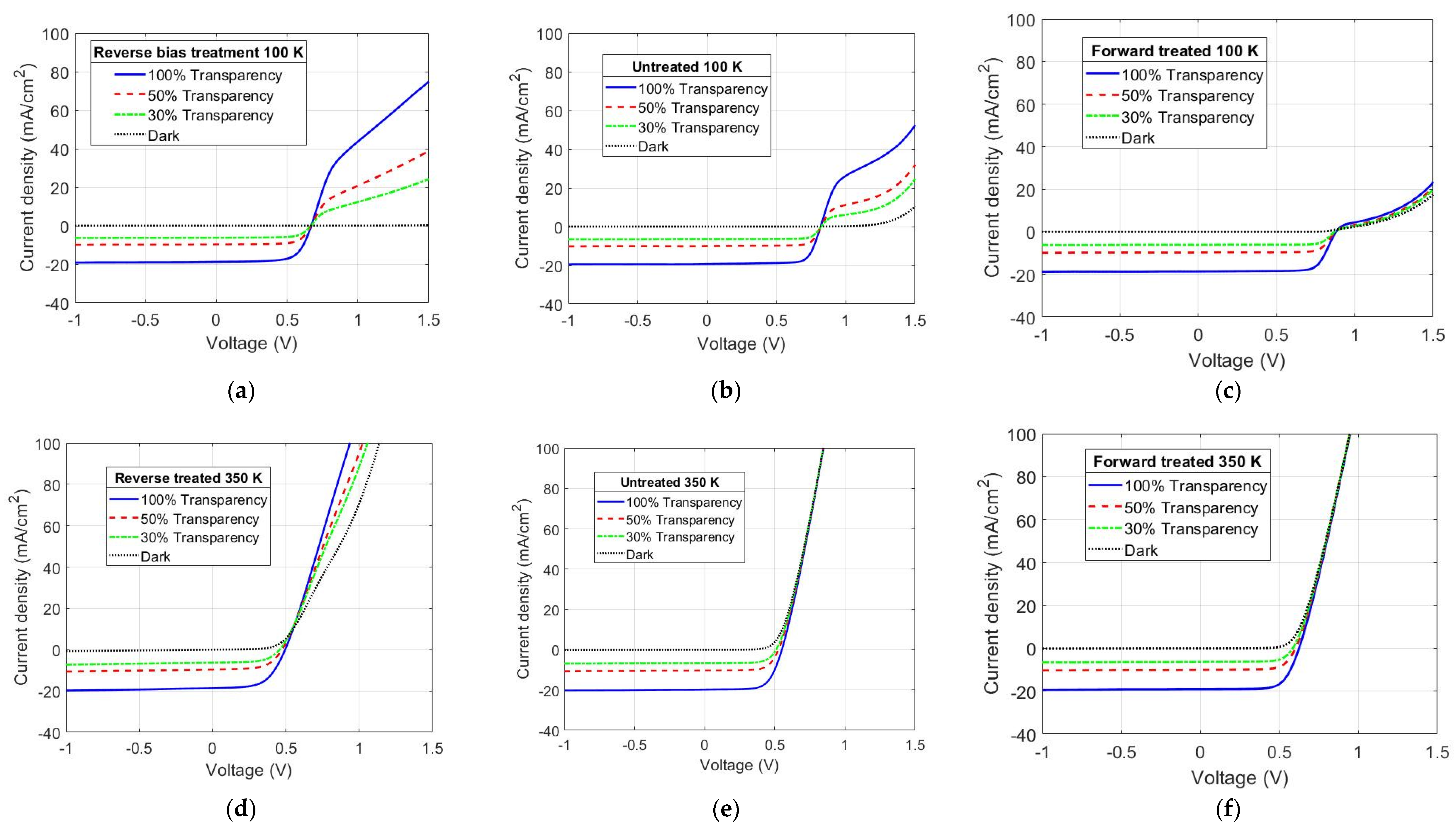
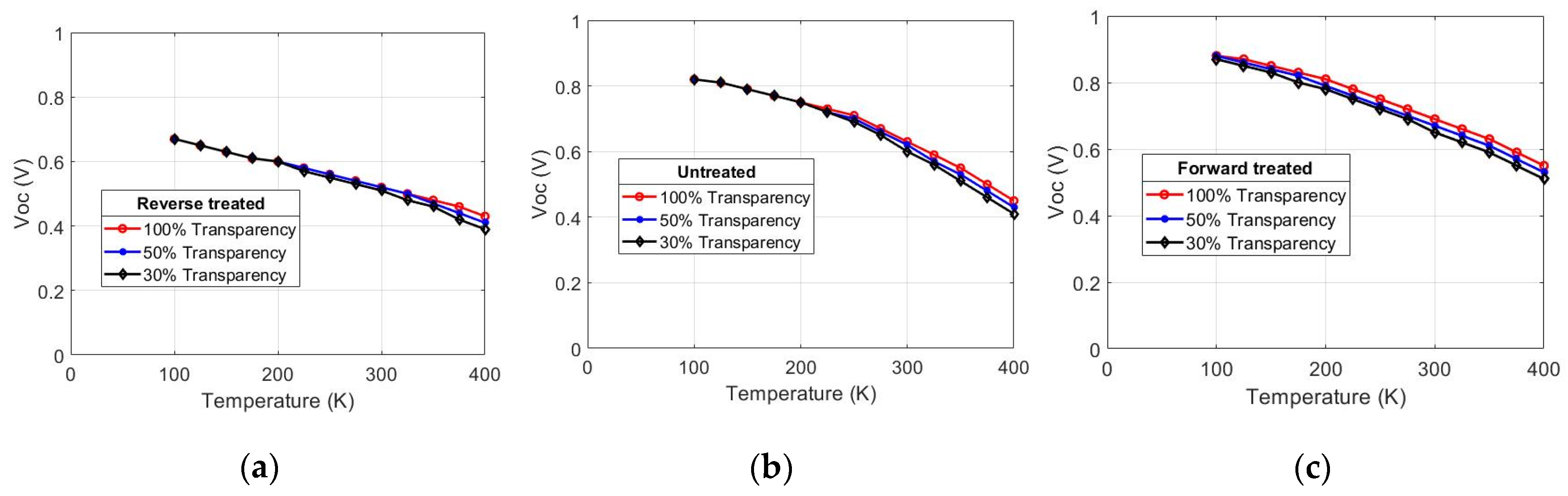
3.1. Experimental Results

Current density–voltage (J–V) curves measured at different temperatures and different illumination values are presented in Figure 2. These curves show that in the lower temperature regime, the current density in the forward bias depends on the applied treatment.
At 100 K, the gain factor of the phototransistor model increases when a reverse-bias treatment is applied to the cell, and the opposite happens with a forward-bias treatment. At 350 K, the superposition principle holds for the untreated sample and the sample treated with forward bias, but not for the reverse bias-treated sample. In the latter, the current density in forward bias still presents a distortion that depends on the illumination level. However, the curves at 100 K also present some interesting behavior. For instance, the sample treated with a forward bias shows a slight exponential increase in the current in forward bias, which could be attributed to the barrier-lowering effect mentioned in the previous chapter due to the strong electric field created by the accumulation of charges at the Mo/CIGS interface. This could also explain the lower exponential or even linear increase in the forward current for the untreated and the reverse-treated samples which have a lower doping level and, in turn, a weaker electric field in the Mo/CIGS junction.
These curves also show another aspect of the phototransistor effect related to the value of Voc. If Voc is different, at a given temperature, for each illumination level, the phototransistor behavior is not present in the cell. On the other hand, if Voc for all illumination levels tends to converge at one point, the J–V curve is influenced by the phototransistor behavior, as described in [35]. In this case, the sample treated in reverse bias shows the phototransistor behavior for a wide range of temperatures, even as high as 300 K, while the sample treated with a forward bias does not show this behavior even in the lower temperature regime, and only in the lowest temperatures (lower than 100 K) can this effect be perceived. The effect of the phototransistor behavior on Voc can be better seen in a Voc vs. temperature plot for all the illumination levels, as visualized in Figure 3.
Figure 4 shows the extrapolation of Voc to 0 K in the low- and high-temperature regimes to obtain the corresponding activation energies. The extrapolated value of Voc to 0 K divided by the elemental charge represents the activation energy. The extrapolation based on the high-temperature regime shows an activation energy of 1.2 eV for both the untreated sample and the sample treated in forward bias. However, for the sample treated with a reverse bias, this activation energy is lower (0.8 eV). This could be attributed to the presence of the phototransistor behavior even at high temperature, which is also evident in Figure 2d.
In the low-temperature regime, Voc does not increase linearly with temperature as in the high-temperature regime. The effect of the back contact barrier, according to [35], is a plausible explanation for this non-linear dependence. The difference between the activation energies extrapolated to 0 K from the high- and the low-temperature regimes corresponds, according to [35], to the height of the potential barrier at the back contact. The untreated sample has an apparent barrier height of 340 meV, and the forward-bias treatment reduces it to 290 meV. These barrier heights calculated from both activation energies could, however, be slightly overestimated as a result of the non-linear dependence of the absorbers bandgap on temperature [47].
For the sample treated in reverse bias, the phototransistor behavior is present even in the high-temperature regime. This makes the calculation of the apparent barrier height based on the activation energies not possible. If an activation energy of 1.2 eV is supposed for the high-temperature regime, as in the other two samples, the calculated barrier height is 460 meV, which represents an increase of more than 100 meV with respect to the untreated sample.
Capacitance profiling also provides information about the causes behind the phototransistor behavior. As shown in Figure 5, the apparent doping level in the absorber calculated from the C–V profile is reduced with the reverse-bias treatment, which partly explains the decrease in Voc. The opposite occurs with the forward-bias treatment.

3.2. Simulation Results

The simulated J–V curves shown in Figure 6 resemble the experimental results of Figure 2. The low-doping high-barrier case (7 × 1014 cm−3 in CIGS and a barrier height of 460 meV for Mo/CIGS) presents the same trend at 100 K as that of Figure 2a, with a saturated current in forward bias and Early effect that leads to an almost linear increase in the current with the applied bias. The current in forward bias also presents a strong dependence on the illumination level. On the other hand, the case with a CIGS doping of 1 × 1016 cm−3 and a barrier of 200 meV, considered as a high-doping low-barrier case from here onwards, presents a much lower gain than the previous case, as well as a more pronounced saturation of the current in forward bias. However, it is possible to see that the current in forward bias does not have a complete linear dependence on the applied voltage but shows a slight exponential increase due to the barrier-lowering effect that was introduced in the model.
Figure 6b presents the intermediate case, with a doping of 1 × 1015 cm−3 and a barrier of 300 meV at 100 K. The gain in this case has an intermediate value between the low-doping high-barrier case and the high-doping low-barrier case. The forward current only exhibits a linear Early effect in contrast with the J–V curve presented in Figure 2b. In Figure 6e, it can be seen that at 300 K, the phototransistor behavior is no longer evident for the intermediate case, as shown in Figure 2e because the superposition principle holds, as well as in the high-doping low-barrier case (Figure 6f).
In Figure 7, Voc curves against temperature are presented similarly to those of Figure 3 for different illumination levels. The three simulation cases were discussed before, namely the low-doping high-barrier case (7 × 1014 cm−3 for CIGS and a barrier of 460 meV), the intermediate case (1 × 1015 cm−3 and 300 meV) and the high-doping low-barrier case (1 × 1016 cm−3 and 200 meV).
It is possible to see in Figure 7a similar behavior as that shown in Figure 3. The low-doping high-barrier case does not exhibit a variation of Voc with temperature in the low-temperature regime, and only at 300 K or higher does Voc depend on the illumination level. In contrast, the intermediate case shows a dependence of Voc on the illumination level over 200 K. Meanwhile, for the high-doping low-barrier case, there is a splitting of Voc with the illumination level in almost the whole range of temperatures that increases linearly with temperature from the lowest temperature where no splitting can be observed.
To calculate the apparent barrier heights of the three simulated cases, the extrapolations of the Voc curves in the low- and high-temperature regimes are required for the illumination level corresponding to 100% transparency. The situation presented in Figure 8 is slightly different when compared to that of Figure 4. For instance, the low-doping high-barrier case exhibits a lower saturation in the high-temperature regime as compared to the reverse bias-treated sample in Figure 4a, and the value of the barrier is 460 meV approximately, as in the experimental case. The intermediate case is closer to the Voc curve of the untreated sample, with a barrier of 330 meV approximately, which is slightly higher than the expected value. The high-doping low-barrier case does not present a saturation of Voc over the whole temperature range, which leads to a barrier height of 150 meV, lower than the expected value.
The effect of the barrier lowering is shown in Figure 9 for two different cases for comparison.
In the high-doping low-barrier case presented in Figure 9b, the barrier-lowering effect is clearly visible as a slight exponential increase in the current with the applied voltage. The situation in Figure 9a for the low-doping high-barrier case is different, as the difference in the current level between the simulation with and without the barrier-lowering model is almost negligible.
Two final simulations are presented to discuss the Early effect and the punch-through effect in CIGS solar cells. These consist on the simulation model presented in Figure 1 but with an absorber thickness of 1.5 µm instead of 2.0 µm to reduce the distance between both SCRs. The low-doping high-barrier case and the high-doping low-barrier case are considered in these two simulations. I–V curves at 100 K are shown in Figure 10 for both cases with different illumination levels.
It is possible to see in Figure 10a how the current exhibits a second exponential increase when the bias is higher than 0.7 V instead of the linear Early effect presented in Figure 6a. The high-doping low-barrier case shown in Figure 9b on the other hand does present an almost linear increase with a slight deviation induced by the barrier-lowering model previously mentioned, although the current density at 1.5 V is higher than that presented for the calculation with a 2 µm absorber thickness in Figure 7c.
To obtain a better understanding of the principle behind the second exponential increase in the current for the low-doping high-barrier case presented in Figure 10a, the band diagram of both cases presented in Figure 10 is shown in Figure 11 at 1.5 V and a transparency of 100%.
The band diagram of the low-doping high-barrier case presents a pronounced bending towards the back contact as shown in Figure 11a, and the flat or quasi-neutral region is very thin. On the other hand, in Figure 11b, the energy bands in the absorber are mostly flat except near the Mo/CIGS interface due to the applied bias, and a large quasi-neutral region is found instead. In the second case, the absorber is not depleted of holes, which means that the hole current in the device should be comparable to the current of electrons. However, in the punch-through effect seen in Figure 11a, the absorber is almost totally depleted of holes, and the electron current is dominant. These two situations can be seen in Figure 12 for the same cases shown in Figure 11 at 100 K and a bias of 1.5 V.
Figure 12b shows that for the high-doping low-barrier case, the electron and hole currents are comparable in magnitude. However, in the low-doping high-barrier case shown in Figure 12a, the electron current is dominant and differs from the hole current by an order of magnitude, which is a feature of the punch-through effect.

4. Discussion

These results provide further evidence of the phototransistor behavior in CIGS solar cells. As previously discussed in [34,35], this behavior depends on the doping level in the absorber and the height of the barrier at the Mo/CIGS interface. These premises are also verified here with the experimental results presented in Figure 2 and the simulations of Figure 6. For instance, the sample treated in reverse bias, which corresponds to the low-doping high-barrier simulation case presented in Figure 2a and Figure 6a, respectively, shows a strong dependence of the current in the forward-bias regime on the illumination level. The gain factor that represents this dependence increases when the doping level of the absorber decreases with respect to that of ZnO/CdS, when the barrier height of the Mo/CIGS junction increases or when the width of the absorber decreases. When a normal transistor is considered, the gain depends on the doping levels of the emitter and the base, on the width of both quasi-neutral regions and on the diffusion lengths of holes and electrons in the emitter and the base, respectively [36]. In CIGS solar cells, the doping level of the absorber was found to decrease when a reverse-bias treatment was applied, and the width of the SCR in CIGS increased at the same time, according to Figure 5; thus, the width of the absorbers quasi-neutral region decreased, which leads to the higher gain factor in the phototransistor model.
Non-idealities of BJT transistors were also found in CIGS solar cells under certain conditions as a side effect of the phototransistor behavior. For instance, the Early effect is clearly visible in Figure 2a,b for experimental results, and also in Figure 6a,b in simulations. An extreme Early effect was found in Figure 10a where the current increases exponentially; this increase can be explained by an almost non-existent quasi-neutral region in the absorber as shown in Figure 11a. This extreme case of the Early effect is known as punch-through, and it implies a very high current flowing between the emitter and collector. In Figure 10a, the current flowing when a bias of 1.5 V is applied in the simulation is around 500 mA/cm2, but with a thinner absorber, it could reach values of 1 × 10⁴ mA/cm2 (not shown), which is an extremely high value.
The phototransistor model in CIGS solar cells presented in [34] considers the Mo/CIGS junction as the collector/base junction, which is a Schottky junction instead of a normal pn junction. The polarity of this junction opposes that of the main pn junction, which leads to a decrease in Voc of the solar cell. This explains the saturation of the Voc curve over temperature found in Figure 3 and Figure 7, because the effect of this Schottky barrier increases when temperature decreases. At low temperatures, depending on the treatment applied to the sample or the parameters considered for the simulation, Voc was found to be independent of the illumination level, which is another indicator of the phototransistor effect [34]. In Figure 3a, for the sample treated in reverse bias, this independence of the illumination level is present over a wide range of temperatures, in contrast with the sample treated in forward bias, where Voc behaves as in a normal pn junction solar cell at temperatures as low as 200 K. The metastable nature of the phototransistor behavior, as a redistribution of charges in the absorber, is also shown in Figure 5. The change in the effective doping also explains the differences in the forward current presented by each sample. A lower net doping level in the absorber, as in the reverse-treated sample case in Figure 5, means a smaller effective base width in the phototransistor model, which, in turn, leads to a higher gain. Moreover, as the net doping level near the Mo/CIGS interface is smaller, the blocking of the current by this junction will be lower. Therefore, the current density in the forward bias under illumination will be higher, as shown in Figure 2a. The opposite situation occurs in the forward-treated sample with a forward bias, as shown in Figure 2c.
However, the simulated Voc curves shown in Figure 8 diverge somewhat from the experimental ones of Figure 4. For instance, the Voc curve of the sample treated in reverse bias in Figure 3a has a smaller slope in the high-temperature regime, which leads to an extrapolated value of 0.8 eV instead of 1.2 eV because the phototransistor behavior was still present in the high-temperature regime. On the other hand, the simulation of the low-doping high-barrier case does not display this saturation of Voc in the high-temperature regime, which leads to an extrapolated value at 0 K slightly higher than 1.2 eV in Figure 8a. The curve of the untreated sample in Figure 4b is in good agreement with the simulation of the intermediate case presented in Figure 8b. Finally, the simulation of the high-doping low-barrier case shows a diminished saturation of Voc in the low-temperature regime in contrast with the results of the sample treated in forward bias, which yields a calculated barrier height that is lower than the defined value (150 meV instead of 200 meV). This could be explained by the barrier-lowering model that was used in the simulations. The extrapolation of the activation energies from the high-temperature regime in the simulations of the intermediate case and the high-doping low-barrier case lead to a value that is around 1.3 eV, which is higher than the defined value of the bandgap (1.2 eV). The temperature dependence of the effective density of states Nc and Nv, according to [48], could explain the difference between both values.
It was already mentioned that a barrier-lowering model for the Mo/CIGS interface was considered to explain some details of the experimental results. An example of this is seen in Figure 2c, with the sample treated in forward bias. This treatment increases the effective doping according to C–V profiles, as shown in Figure 5, through a metastable redistribution of charges, and the apparent barrier height that is calculated from I–V–T measurements is decreased at the same time. These two changes also lead to a higher effective width of the base, and the result is a lower gain of the phototransistor in the model, but also a lower current in forward bias. However, a less pronounced Early effect and a more saturated forward current density are expected as a result of the lower gain and the higher doping, which Figure 2c seems to contradict. Instead, these curves present a slight exponential increase in the current density with a forward bias. The need for a mechanism that reconciles both findings in the experimental J–V curves can be solved with the barrier lowering, because this mechanism is independent of the base width of the phototransistor, and also explains the non-linear increase in the forward current density with the applied bias, as shown in Figure 9. The J–V curves of the untreated sample in Figure 2b exhibit more pronounced phototransistor behavior, but also a non-linear increase in the forward current density with the applied bias; the reason behind this increase could be attributed to a non-linear Early effect, but also to the barrier lowering at the Mo/CIGS interface. In this case, the barrier-lowering mechanism seems a better explanation regarding this non-linear increase in the forward current in the untreated sample, because the sample treated with reverse bias only shows a linear Early effect with a lower effective doping and a higher calculated apparent barrier height. The simulated I–V curve of the intermediate case in Figure 6b only exhibits a linear Early effect in contrast with the experimental results of the untreated samples in Figure 2b. In this case, the doping concentration used in the simulations for the absorber is not sufficiently high for the barrier lowering to be significant, but it is high enough to prevent a non-linear Early effect due to a reduced effective width of the base.

5. Conclusions

The aim of this paper is to further discuss the phototransistor behavior in CIGS solar cells and how it is affected by the back contact barrier; the phototransistor model explains the behavior of the I–V curves in low-temperature measurements. Experimental and numerical simulation results were presented to support this model and expand it with the incorporation of additional elements, such as the barrier-lowering effect and the impact of the metastabilities on the phototransistor behavior. The key findings are:
  • The gain factor of the phototransistor model, as seen in the I–V curves, is affected differently depending on the applied treatment. A forward-bias and high-temperature treatment (+0.4 V and 100 °C) reduces the gain while a reverse-bias treatment (−0.4 V and 100 °C) increases it.
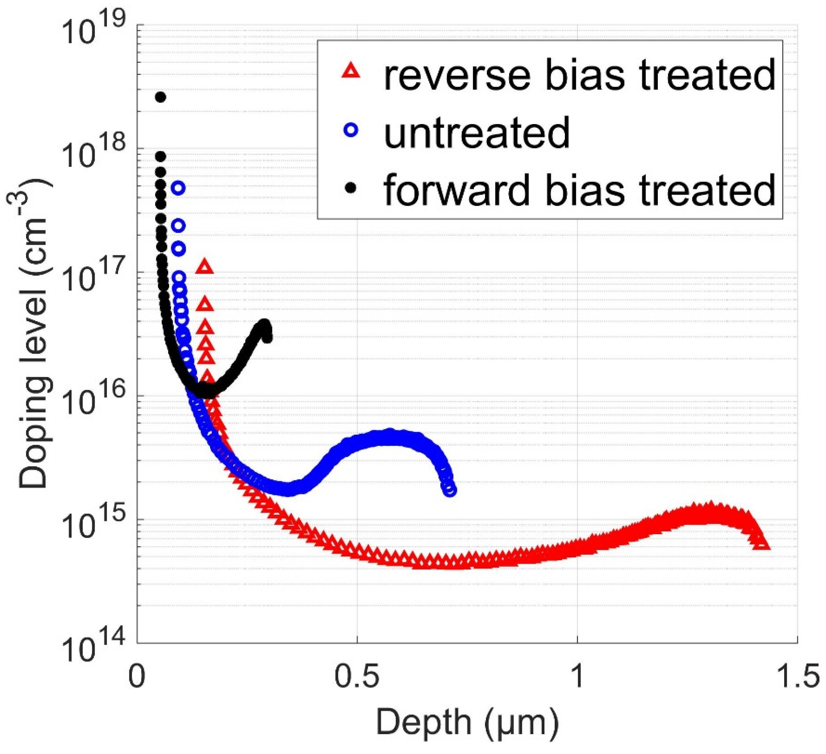
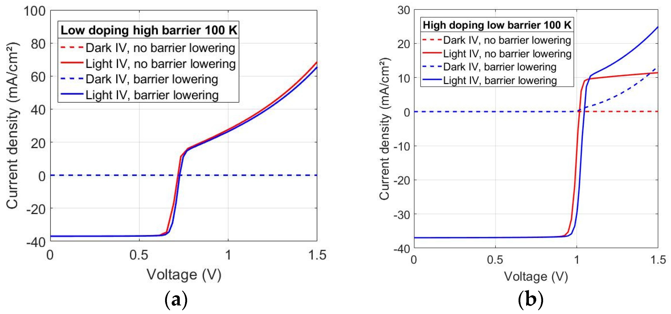
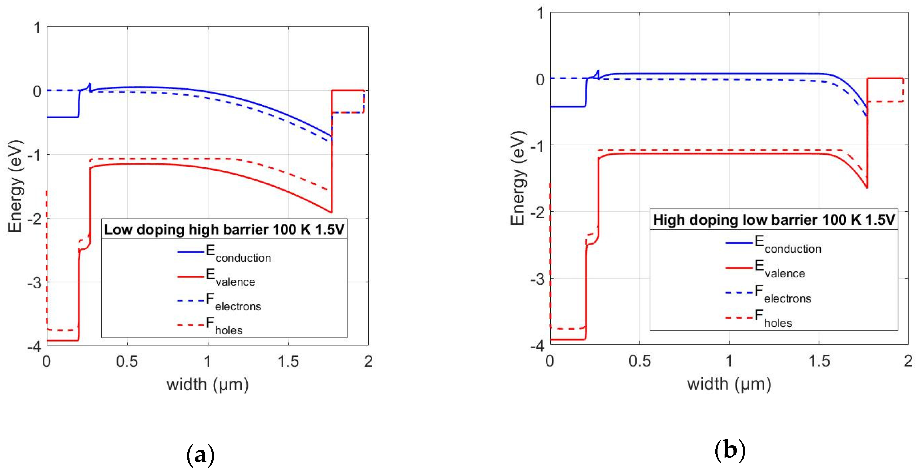
  • The change in the gain of the phototransistor is directly related to a metastable redistribution of charges in the absorber and the apparent height of the back-contact barrier. In particular, the forward-bias treatment increases the apparent doping level of CIGS and decreases the barrier height, while the reverse-bias treatment does the opposite.
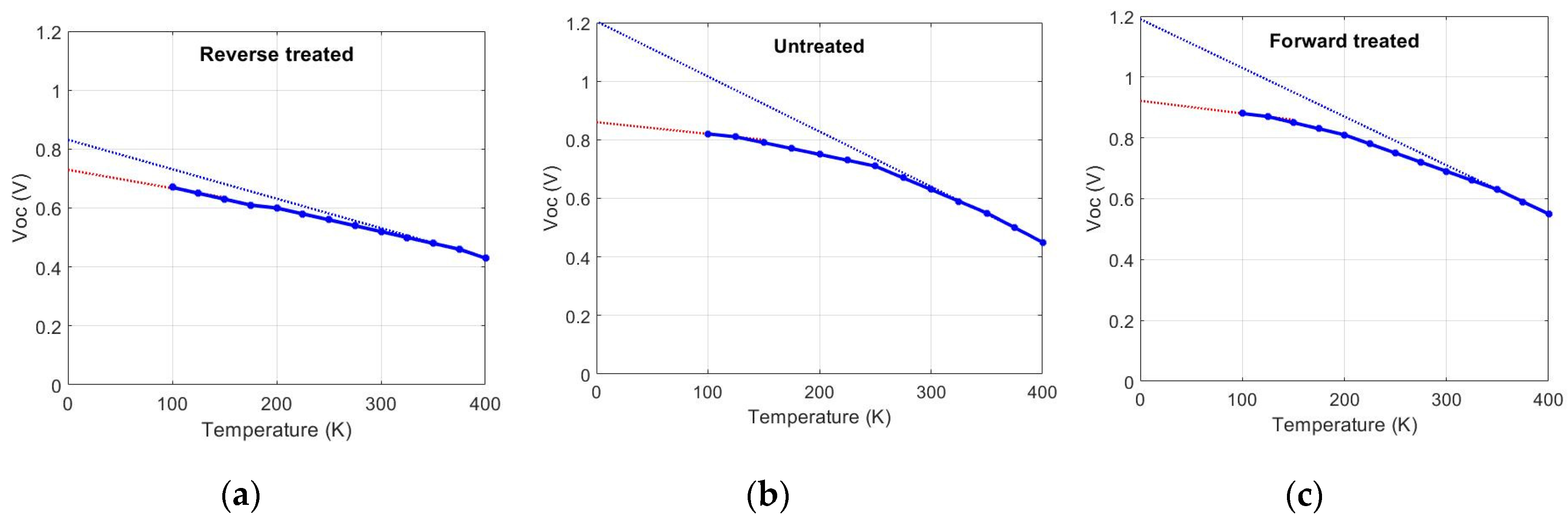
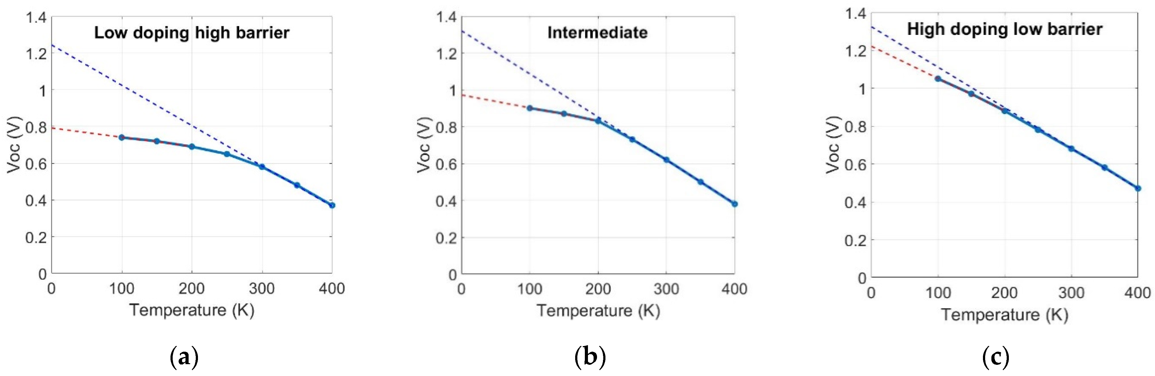
  • It could be shown in this paper how metastabilities induced by different treatments affect other aspects of the phototransistor model. Two of the affected aspects are as follows: (i) how the value of Voc saturates, instead of linearly increasing, when the temperature decreases, and (ii) how Voc does not depend on the illumination level. The reverse-bias treatment extends this temperature range even up to 400 K. The forward-bias treatment, on the other hand, reduces this temperature range.
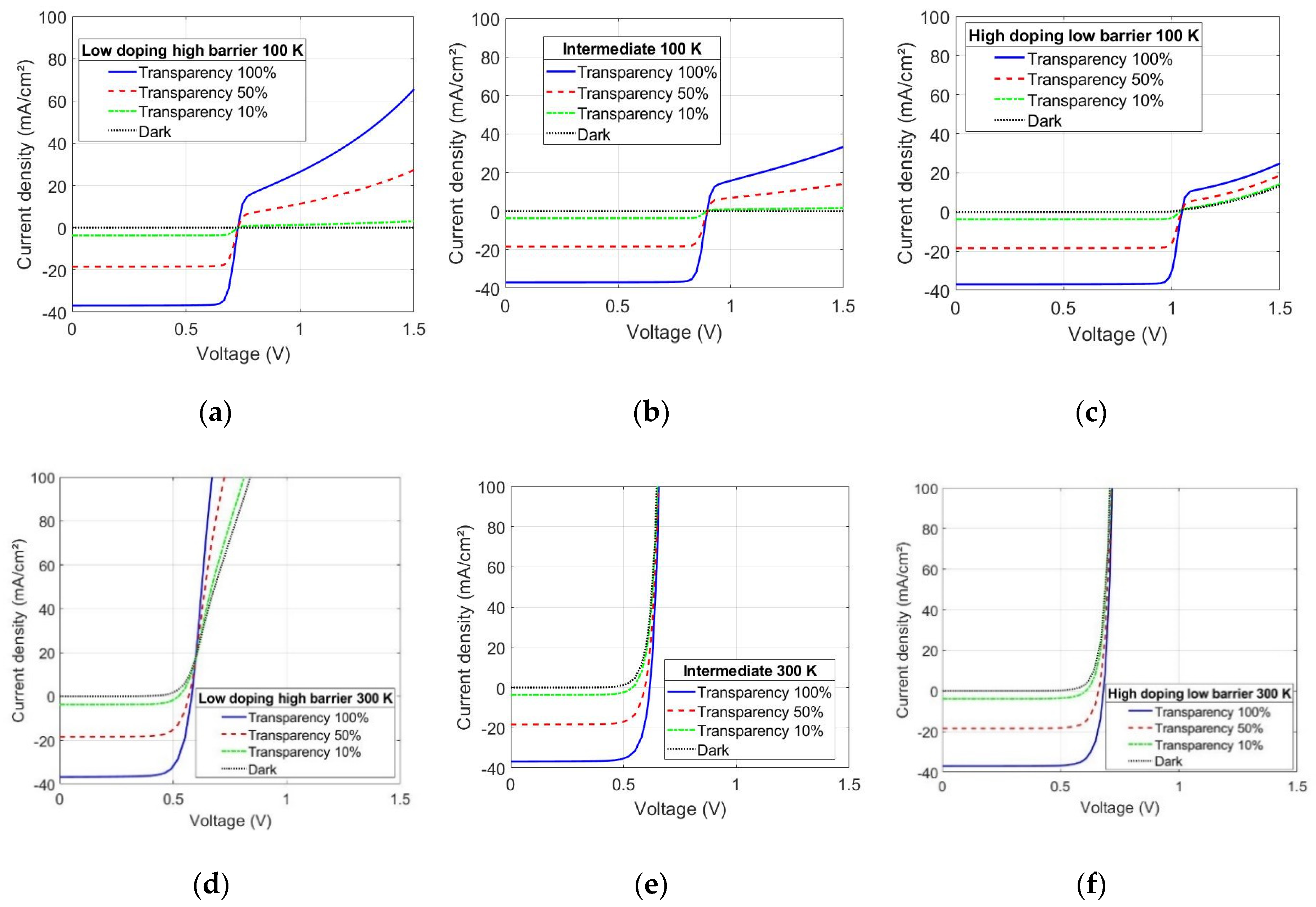
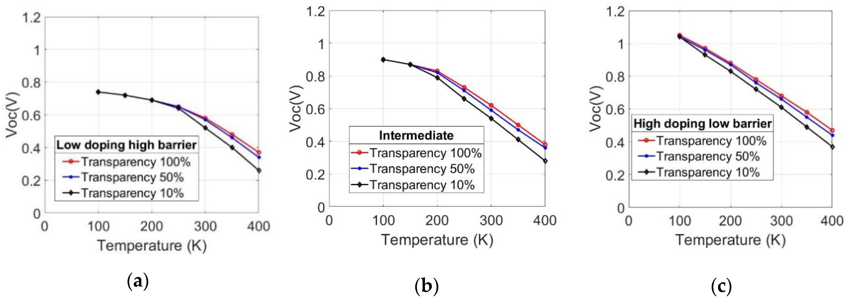
  • Numerical simulations of a thin-film CIGS device model are in good agreement with the experimental results; a lower doping level in CIGS in combination with a higher back contact barrier increases the gain factor of the phototransistor, while a high doping level with a lower barrier decreases it.
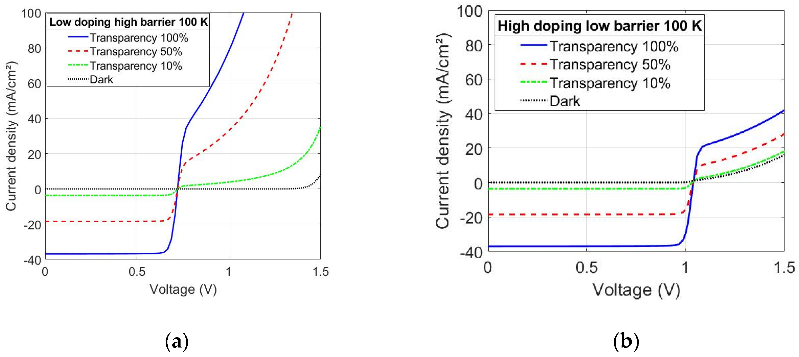
  • The barrier-lowering effect is necessary in order to explain the slight exponential increase in the saturated current density under forward bias that is found in low-temperature I–V measurements for the forward-treated sample. Without the barrier-lowering behavior, a linear Early effect is predicted by the simulation of the corresponding case (high-doping, low-barrier).
  • The punch-through effect was found to affect devices with thin and low-doping absorbers, as both SCRs overlap. The consequence is a rapid increase in the electron current, affecting Voc in turn.
There are, however, some issues that should be addressed in further research. For instance, the dependence of the bandgap energy on temperature could also affect the Voc (T) curves, as has been mentioned in the Results Section, which, in turn, affects the calculated barrier heights. Furthermore, the origin of the barrier-lowering effect is also not clear, as both the force of the image charges and tunneling could be plausible explanations for it. The research results presented in this paper could be extended by considering the characteristics of more complex devices, such as gradients of the absorbers bandgap and doping, or how CIGS solar cells produced by different processes (such as sequential processes) are affected by the metastabilities induced by different treatments with respect to the phototransistor behavior. Moreover, the phototransistor model only deals with a specific barrier in the CIGS solar cell, the back contact one; other barriers such as the band offset in the CdS/CIGS interface or a bandgap gradient in the absorber may affect the behavior of the solar cell in a manner that is not considered in this work. Finally, other degradation mechanisms such as PID or damp heat might induce other unexpected behavior of the I–V curves at low temperatures.

Author Contributions

Conceptualization, R.V.L. and T.W.; methodology, R.V.L. and T.W.; software, R.V.L.; validation, D.F.M., D.M., T.L. and O.S.; formal analysis, R.V.L.; investigation, R.V.L.; resources, T.W. and R.S.; data curation, R.V.L.; writing—original draft preparation, R.V.L.; writing—review and editing, D.F.M., T.L., D.M. and O.S.; visualization, T.W.; supervision, T.W. and D.F.M.; project administration, T.W. and R.S.; funding acquisition, T.W. and R.S. All authors have read and agreed to the published version of the manuscript.

Funding

This research was funded by the German Ministry of Energy and Economics under contract number 0324070 (proCIGS).

Acknowledgments

The authors acknowledge the support of the University of Applied Sciences of Ulm (THU) and Universidad Politecnica de Madrid, the CIGS team at ZSW and the NICE Solar GmbH team in the development of this work.

Conflicts of Interest

The authors declare no conflict of interest. The funders had no role in the design of the study; in the collection, analyses, or interpretation of data; in the writing of the manuscript, or in the decision to publish the results.

References

  1. Nakamura, M.; Yamaguchi, K.; Kimoto, Y.; Yasaki, Y.; Kato, T.; Sugimoto, H. Cd-Free Cu(In,Ga)(Se,S)2 Thin-Film Solar Cell With Record Efficiency of 23.35%. IEEE J. Photovolt. 2019, 9, 1863–1867. [Google Scholar] [CrossRef]
  2. Stoelzel, M.; Algasinger, M.; Zelenina, A.; Weber, A.; Sode, M.; Schubbert, C.; Eraerds, P.; Lechner, R.; Dalibor, T.; Palm, J. Absorber Optimization in CIGSSe Modules with a Sputtered ZnOS Buffer Layer at 19% Efficiency. In Proceedings of the 36th European Photovoltaic Solar Energy Conference and Exhibition, Marseille, France, 9 September 2019. [Google Scholar] [CrossRef]
  3. Zhu, H.; Niu, X.; Wan, M.; Mai, Y. A study of ZnO:Al thin films reactively sputtered under the control of target voltage for application in Cu(In,Ga)Se2 thin film solar cells. Vacuum 2019, 161, 297–305. [Google Scholar] [CrossRef]
  4. Zhang, W.; Demirkan, K.; Zapalac, G.; Spaulding, D.; Titus, J.; Mackie, N. Optimizing CdS Buffer Layer For CIGS Based Thin Film Solar Cell. In Proceedings of the 44th Photovoltaic Specialist Conference (PVSC), Washington, DC, USA, 25–30 June 2017. [Google Scholar] [CrossRef]
  5. Garris, R.L.; Mannsfield, L.M.; Egaas, B.; Ramanathan, K. Low-Cd CIGS Solar Cells Made With a Hybrid CdS/Zn(O,S) Buffer Layer. IEEE J. Photovolt. 2017, 7, 281–285. [Google Scholar] [CrossRef]
  6. Kim, S.; Mina, M.S.; Kim, K.; Gwak, J.; Kim, J. Application of a Sn4+ doped In2S3 thin film in a CIGS solar cell as a buffer layer. Sustain. Energy Fuels 2020, 4, 362–368. [Google Scholar] [CrossRef]
  7. Peterson, J.; Torndahl, T.; Platzer-Bjorkman, C.; Hultqvist, A.; Edoff, M. The Influence of Absorber Thickness on Cu(In,Ga)Se2 Solar Cells With Different Buffer Layers. IEEE J. Photovolt. 2013, 3, 1376–1382. [Google Scholar] [CrossRef]
  8. Edoff, M.; Chen, W.C.; Gordon, I.; Vermang, B.; Bolt, P.J.; Deelen, J.; Simor, M.; Flandre, D.; Lontchi, J.; Kovacic, M.; et al. Ultrathin CIGS Solar Cells with Passivated and Highly Reflective Back Contacts—Results from the ARCIGS-M Consortium. In Proceedings of the 36th European Photovoltaic Solar Energy Conference and Exhibition, Marseille, France, 9 September 2019. [Google Scholar] [CrossRef]
  9. Kamikawa-Shimizu, Y.; Shimada, S.; Watanabe, M.; Yamada, A.; Sakurai, K.; Ishizuka, S.; Komaki, H.; Matsubara, K.; Shibata, H.; Tampo, H.; et al. Effects of Mo back contact thickness on the properties of CIGS solar cells. Phys. Status Solidi 2009, 206, 1063–1066. [Google Scholar] [CrossRef]
  10. Nakada, T.; Iga, D.; Ohbo, H.; Kunioka, A. Effects of sodium on Cu(In,Ga)Se2-based thin films and solar cells. Jpn. J. Appl. Phys. 1997, 36, 732–737. [Google Scholar] [CrossRef]
  11. Hariskos, D.; Hempel, W.; Menner, R.; Witte, W. Influence of Substrate Temperature during InxSy Sputtering on Cu(In,Ga)Se2/Buffer Interface Properties and Solar Cell Performance. Appl. Sci. 2020, 10, 1052. [Google Scholar] [CrossRef] [Green Version]
  12. Theelen, M.; Barreau, N.; Hans, V.; Steijvers, H.; Vroon, Z.; Zeman, M. Degradation of CIGS solar cells due to the migration of alkali-elements. In Proceedings of the 42nd Photovoltaic Specialist Conference (PVSC), New Orleans, LA, USA, 14–19 June 2015. [Google Scholar] [CrossRef]
  13. Salomon, O.; Hempel, W.; Kiowski, O.; Lotter, E.; Witte, W.; Ferati, A.; Schneikart, A.; Kaune, G.; Schäffler, R.; Becker, M.; et al. Influence of Molybdenum Back Contact on the PID Effect for Cu(In,Ga)Se2 Solar Cells. Coatings 2019, 9, 794. [Google Scholar] [CrossRef] [Green Version]
  14. Muzzillo, C.P.; Glynn, S.; Hacke, P.; Moutinho, H.R.; Young, M.R.; Teeter, G.; Repins, I.L.; Mansfield, L.M. Potential-Induced Degradation of Cu(In,Ga)Se2 Solar Cells: Alkali Metal Drift and Diffusion Effects. IEEE J. Photovolt. 2018, 8, 1337–1342. [Google Scholar] [CrossRef]
  15. Siebentritt, S. What Limits the Efficiency of Chalcopyrite Solar Cells? Sol. Energy Mater. Sol. Cells 2011, 95, 1471–1476. [Google Scholar] [CrossRef]
  16. Kato, T.; Kitani, K.; Tai, K.F.; Kamada, R.; Hiroi, H.; Sugimoto, H. Characterization of the Back Contact of CIGS Solar Cell as the Origin of “Rollover” Effect. In Proceedings of the 32nd European Photovoltaic Solar Energy Conference and Exhibition, Munich, Germany, 21–24 June 2016. [Google Scholar] [CrossRef]
  17. Hsiao, K.-J.; Liu, J.-D.; Hsieh, H.-H.; Jiang, T.-S. Electrical Impact of MoSe2 on CIGS Thin-Film Solar Cells. Phys. Chem. Chem. Phys. 2013, 15, 18174. [Google Scholar] [CrossRef] [PubMed]
  18. Eisenbarth, T.; Unold, T.; Caballero, R.; Kaufmann, C.A.; Schock, H.-W. Interpretation of Admittance, Capacitance-Voltage, and Current-Voltage Signatures in Cu(In,Ga)Se2 Thin Film Solar Cells. J. Appl. Phys. 2010, 107, 34509. [Google Scholar] [CrossRef]
  19. Rockett, A.; van Duren, J.K.J.; Pudov, A.; Shafarman, W.N. First Quadrant Phototransistor Behavior in CuInSe2 Photovoltaics. Sol. Energy Mater. Sol. Cells 2013, 118, 141–148. [Google Scholar] [CrossRef]
  20. Theys, B.; Klinkert, T.; Mollica, F.; Leite, E.; Donsanti, F.; Jubault, M.; Lincot, D. Revisiting Schottky Barriers for CIGS Solar Cells: Electrical Characterization of the Al/Cu(InGa)Se2 Contact. Phys. Status Solidi 2016, 213, 2425–2430. [Google Scholar] [CrossRef]
  21. Sites, J.R. Quantification of Losses in Thin-Film Polycrystalline Solar Cells. Sol. Energy Mater. Sol. Cells 2003, 75, 243–251. [Google Scholar] [CrossRef]
  22. Roland, P.J.; Bhandari, K.P.; Ellingson, R.J. Electronic Circuit Model for Evaluating S-Kink Distorted Current-Voltage Curves. In Proceedings of the 43rd Photovoltaic Specialists Conference (PVSC), Portland, OR, USA, 5–10 June 2016. [Google Scholar] [CrossRef]
  23. Muecke, D.; Lavrenko, T.; Lorbada, R.V.; Walter, T. On the Determination of the Back Contact Barrier Height of Cu(In,Ga)(S,Se)2 Thin Film Solar Cells. In Proceedings of the 7th World Conference on Photovoltaic Energy Conversion (WCPEC) (A Joint Conference of 45th IEEE PVSC, 28th PVSEC & 34th EU PVSEC), Waikoloa Village, HI, USA, 10–15 June 2018. [Google Scholar] [CrossRef]
  24. Macielak, K.; Igalson, M.; Spiering, S. Comparison of Metastabilities in CIGS Solar Cells with In2S3 and CdS Buffer Layers. In Proceedings of the 37th IEEE Photovoltaic Specialists Conference, Seattle, WA, USA, 19–24 June 2011. [Google Scholar] [CrossRef]
  25. Igalson, M.; Bodegård, M.; Stolt, L.; Jasenek, A. The “defected Layer” and the Mechanism of the Interface-Related Metastable Behavior in the ZnO/CdS/Cu(In,Ga)Se2 Devices. Thin Solid Films 2003, 431–432, 153–157. [Google Scholar] [CrossRef]
  26. Igalson, M.; Zabierowski, P.; Prządo, D.; Urbaniak, A.; Edoff, M.; Shafarman, W.N. Understanding Defect-Related Issues Limiting Efficiency of CIGS Solar Cells. Sol. Energy Mater. Sol. Cells 2009, 93, 1290–1295. [Google Scholar] [CrossRef]
  27. Igalson, M.; Cwil, M.; Edoff, M. Metastabilities in the Electrical Characteristics of CIGS Devices: Experimental Results vs Theoretical Predictions. Thin Solid Films 2007, 515, 6142–6146. [Google Scholar] [CrossRef]
  28. Scheer, R.; Schock, H.-W. Chalcogenide Photovoltaics; Wiley-VCH Verlag GmbH & Co. KGaA: Weinheim, Germany, 2013. [Google Scholar] [CrossRef]
  29. Lany, S.; Zunger, A. Light- and Bias-Induced Metastabilities in Cu(In,Ga)Se2 Based Solar Cells Caused by the (VSe-VCu) Vacancy Complex. J. Appl. Phys. 2006, 100, 113725. [Google Scholar] [CrossRef] [Green Version]
  30. Ott, T.; Walter, T.; Hariskos, D.; Kiowski, O.; Schaffler, R. Accelerated Aging and Contact Degradation of CIGS Solar Cells. In Proceedings of the IEEE 38th Photovoltaic Specialists Conference (PVSC), Austin, TX, USA, 3–8 June 2012. [Google Scholar] [CrossRef]
  31. Nakada, T.; Kunioka, A. Sequential Sputtering/Selenization Technique for the Growth of CuInSe2 Thin Films. Jpn. J. Appl. Phys. 1998, 37, L1065–L1067. [Google Scholar] [CrossRef]
  32. Bronzoni, M.; Colace, L.; De Iacovo, A.; Laudani, A.; Lozito, G.; Lucaferri, V.; Radicioni, M.; Rampino, S. Equivalent Circuit Model for Cu(In,Ga)Se2 Solar Cells Operating at Different Temperatures and Irradiance. Electronics 2018, 7, 324. [Google Scholar] [CrossRef] [Green Version]
  33. Demtsu, S.H.; Sites, J.R. Effect of Back-Contact Barrier on Thin-Film CdTe Solar Cells. Thin Solid Films 2006, 510, 320–324. [Google Scholar] [CrossRef]
  34. Ott, T.; Walter, T.; Unold, T. Phototransistor Effects in Cu(In,Ga)Se2 Solar Cells. Thin Solid Films 2013, 535, 275–278. [Google Scholar] [CrossRef]
  35. Ott, T.; Schönberger, F.; Walter, T.; Hariskos, D.; Kiowski, O.; Salomon, O.; Schäffler, R. Verification of Phototransistor Model for Cu(In,Ga)Se2 Solar Cells. Thin Solid Films 2015, 582, 392–396. [Google Scholar] [CrossRef]
  36. Sze, S.M.; Ng, K.K. Physics of Semiconductor Devices, 3rd ed.; John Wiley & Sons, Inc.: Hoboken, NJ, USA, 2006. [Google Scholar] [CrossRef] [Green Version]
  37. Ott, T.; Walter, T.; Schäffler, R.; Fecht, H.-J. Punch-Through Effect in CIGS Thin Film Solar Cells. In Proceedings of the 32nd European Photovoltaic Solar Energy Conference and Exhibition, Munich, Germany, 21–24 June 2016. [Google Scholar] [CrossRef]
  38. Roussillon, Y.; Karpov, V.G.; Shvydka, D.; Drayton, J.; Compaan, A.D. Back Contact and Reach-through Diode Effects in Thin-Film Photovoltaics. J. Appl. Phys. 2004, 96, 7283–7288. [Google Scholar] [CrossRef]
  39. Mack, P.; Ott, T.; Walter, T.; Hariskos, D.; Schäffler, R. Optimization of Reliability and Metastability of CIGS Solar Cell Parameters. In Proceedings of the 25th European Photovoltaic Solar Energy Conference and Exhibition/5th World Conference on Photovoltaic Energy Conversion, Valencia, Spain, 6–10 September 2010. [Google Scholar] [CrossRef]
  40. Walter, T. Admittance Spectroscopy. In Capacitance Spectroscopy of Semiconductors; Li, J.V., Ferrari, G., Eds.; Jenny Stanford Publishing: Singapore, 2018; pp. 154–196. [Google Scholar] [CrossRef]
  41. Labotec. Available online: http://www.labotec.co.za/wp-content/uploads/2016/07/WTL-WKL-Compact-Chambers-Brochure.pdf (accessed on 5 August 2020).
  42. Tektronix. Available online: https://www.tek.com/document/brochure/model-4200-scs-semiconductor-characterization-system (accessed on 5 August 2020).
  43. Oxford Instruments Nanoscience. Available online: https://nanoscience.oxinst.com/products/cryostats-for-spectroscopy/optistatdn-v (accessed on 5 August 2020).
  44. Keysight. Available online: https://www.keysight.com/en/pd-153734-pn-4155C/semiconductor-parameter-analyzer (accessed on 5 August 2020).
  45. Keysight. Available online: https://www.keysight.com/de/pd-330690-pn-4192A/lf-impedance-analyzer-5-hz-to-13-mhz (accessed on 5 August 2020).
  46. Synopsys. Available online: https://www.synopsys.com/silicon/tcad.html (accessed on 5 August 2020).
  47. Levcenco, S.; Doka, S.; Tezlevan, D.; Marrón, D.F.; Kulyuk, L.; Schedel-Niedrig, T.; Lux-Steiner, M.C.; Arushanov, E. Temperature dependence of the exciton gap in monocrystalline CuGaS2. Physica B 2010, 405, 3547–3550. [Google Scholar] [CrossRef]
  48. Elanzeery, H.; Babbe, F.; Melchiorre, M.; Werner, F.; Siebentritt, S. High-Performance Low Bandgap Thin Film Solar Cells for Tandem Applications. Prog. Photovolt. Res. Appl. 2018, 26, 437–442. [Google Scholar] [CrossRef] [Green Version]
Figure 1. Model of the solar cell stack used in the simulations.
Energies 13 04753 g001
Figure 2. Measured J–V curves with different illumination values. Plots (ac) correspond to the sample treated with a reverse bias, the non-treated sample and the sample treated with a forward bias, respectively, at 100 K. Plots (df) correspond to the previously indicated samples, respectively, at 350 K. J–V results with different transmission filters are also shown.
Energies 13 04753 g002
Figure 3. Open-circuit voltage (Voc) vs. temperature plot. In (a), the sample treated with a reverse bias. In (b) the non-treated sample. In (c), the sample treated with a forward bias. In all three cases, the Voc is plotted for each illumination level according to the transparency of the optical filter.
Energies 13 04753 g003
Figure 4. Voc against temperature plots for (a) the reverse bias-treated sample, (b) the untreated sample and (c) the forward bias-treated sample with the highest illumination level (100% transparency). For each curve, a trendline is included in both the low- (red) and high- (blue) temperature regime to extrapolate the value of Voc to 0 K.
Energies 13 04753 g004
Figure 5. Curves of the apparent doping level against the depth of the space charge region at 300 K for the untreated sample and the samples treated in forward and reverse bias.
Energies 13 04753 g005
Figure 6. Simulated current density–voltage (J–V) curves at 100 K for (a) CIGS doping of 7 × 1014 cm−3 and a barrier of 460 meV, (b) doping of 1 × 1015 cm−3 and barrier of 300 meV and (c) doping of 1 × 1016 cm−3 and barrier of 200 meV. The same parameters are considered in (ce), respectively, for the simulations at 300 K.
Energies 13 04753 g006
Figure 7. Voc against temperature plot for (a) the low-doping high-barrier case, (b) the intermediate case, and (c) the high-doping low-barrier case with transparency values of 100, 50 and 10%.
Energies 13 04753 g007
Figure 8. Voc against temperature plots for (a) the low-doping high-barrier case, (b) the intermediate case and (c) the high-doping low-barrier case with the highest illumination level (100% transparency). The extrapolations of Voc to 0 K in the low- and high-temperature regime are shown in red and blue dotted lines, respectively.
Energies 13 04753 g008
Figure 9. Simulated J–V curves at 100 K for (a) the low-doping high-barrier case and (b) the high-doping low-barrier case with no barrier lowering (red) and with barrier lowering (blue), and with 100% illumination (continuous lines) and 0% illumination level (dotted lines).
Energies 13 04753 g009
Figure 10. Simulated I–V curves at 100 K for (a) the low-doping high-barrier case and (b) the high-doping low-barrier case with an absorber thickness of 1.5 µm with 100%, 50% and 10% transparency.
Energies 13 04753 g010
Figure 11. Simulated band diagrams at 100 K, a bias of 1.5 V and a transparency of 100% (a) for the low-doping high-barrier case and (b) for the high-doping low-barrier case. An absorber thickness of 1.5 µm is defined in both cases.
Energies 13 04753 g011
Figure 12. Simulated electron and hole currents at 100 K, a bias of 1.5 V and a transparency of 100% in a 1.5 µm thick absorber (a) for the low-doping high-barrier case and (b) for the high-doping low-barrier case over the whole length of the device.
Energies 13 04753 g012
Table 1. Physical properties of each material layer in the simulation model.
LayerDoping Level (cm−3)Bandgap (eV)Electron Affinity (eV)Mobility e/h (cm2/Vs)Thickness (µm)
Mo--5.6–5.3 1-0.2
CIGS7 × 1014–1 × 10161.24.6100/251.5–2.0
CdS1 × 10172.54.5100/250.05
ZnO1 × 10203.44.6100/250.2
1 The electron affinity of Mo is represented instead by the work function of this material.

