Article

Comparative Study of Control Strategies for Stabilization and Performance Improvement of DC Microgrids with a CPL Connected

by
Isaías V. de Bessa
*,
Renan L. P. de Medeiros
*,
Iury Bessa
*,
Florindo A. C. Ayres Junior
*,
Alessandra R. de Menezes
,
Gustavo M. Torres
and
João Edgar Chaves Filho
Department of Electricity, Federal University of Amazonas, Manaus-AM 69080-900, Brazil
*
Authors to whom correspondence should be addressed.
Energies 2020, 13(10), 2663; https://doi.org/10.3390/en13102663
Submission received: 28 April 2020 / Revised: 15 May 2020 / Accepted: 15 May 2020 / Published: 25 May 2020
(This article belongs to the Special Issue Microgrids 2020)

Abstract

:
The DC microgrid system is composed by converters that operate like feeders and loads. Among these loads, we highlight the constant power loads (CPLs) that may cause instability in the microgrid, observed in the form of undesired oscillations due to its negative impedance behavior. Therefore, this work proposes to use performance indices and stability margins to evaluate state and output feedback control strategies for stabilization of DC microgrids. In particular, it is proposed to evaluate the stability margin of the proposed methodologies by means of the impedance relations in the microgrid based on the Middlebrook criterion. Our simulations and tests showed the relation between the performance and stability degradation and the microgrid impedances variation.

1. Introduction

In DC distribution systems, the voltage regulation of the generation system is carried out by isolated and non-isolated power converters with classic topologies, e.g., buck and boost. The modeling of DC-DC converters is based on the average space model (ASM) as described in [1,2,3,4] leading to a non-linear model that is usually linearized around an operating point for using linear design tools.
In particular, a DC microgrid is a set of energy supply elements connected to loads. The power generation is provided by either renewable sources or through traditional generation. In addition, the DC microgrids can operate on- or off-grid [5,6,7,8,9,10]. In [5], an off-grid microgrid model is proposed where the voltage and frequency transients are evaluated by means of frequency analysis. In [8], an overview of design, control, operation, stability and protection of DC systems is provided. Similarly, [7,11] review stability criteria applied to DC microgrids to design the elements of the distribution system. In [10], a decentralized control algorithm for DC microgrids is proposed.
A relevant stability issue when connecting power converters into a DC microgrid is the negative impedance effect that results in undesired oscillations due to the interaction of an input converter with an output converter operating as a constant power load (CPL) [7,9,12,13,14,15]. In [9,15], methods to dampen the oscillations due to the connection between CPL and microgrid are presented as passive damping techniques, which performs as the design of RL or RC filters to lessen the effect of the oscillation; or active damping techniques that perform damping modification using control techniques on the load or feeder. In addition, [12] uses predictive control to perform active oscillation damping. In [16] it is investigated the voltage regulation of a microgrid connected to a CPL, obtaining robust performance conditions to ensure the regulation the existence of an equilibrium point.
These papers [2,17,18,19,20,21] used control strategies based on large-signal model (LSM) for stabilization of microgrids. The authors in [2] propose a decoupled ASM for buck, boost and buck-boost converters where the sub-modules are compensated through first-order controllers. In [17,18], a microgrid regulated by a boost converter connected to a CPL such that the oscillations are dampened through sliding mode control (SMC), while in [20], a comparative analysis of the performance of the SMC and Lyapunov redesign controller (LRC) techniques is performed under CPL power variation. In [19,21], a Lyapunov-based stability analysis for large signals is performed to estimate stability regions.
Among the stabilization strategies for microgrids connected to CPLs, the application of robust [3,22,23] and predictive [24,25,26,27] control techiniques stands out. In particular, [3] proposes a robust control technique to deal with parametric uncertainties and CPL power variation. In [22], a robust SMC is proposed to guarantee the stability of the system. Furthermore, a mathematical modeling and robust control approach for power converters operating with CPLs in continuous conduction mode (CCM) is described in [23,28,28]. In [25], the authors propose the motor speed control of a distal generator, verifying the performance of this controller under several conditions, among them, when connected to CPL, while [26] uses an extended Kalman filter to perform model predictive control for mitigation of oscillations based on the estimates of the feeder capacitor voltage. In [19] an stability analysis is performed on microgrids based on LSM of DC-DC, DC-AC and AC-DC converters.
Robust stabilization and performance are also addressed in the literature [29,30,31]. In [29], several control strategies such as distributed, optimal and robust are used for voltage regulation of a DC microgrid with multiple DC-DC converters aiming to meet a power sharing criteria. In [30], a networked control strategy is applied in a delayed system by using Smith predictor to compute state feedback controller gains. In [31], an optimal and robust nonlinear control scheme is applied in a DC microgrid for achieving trajectory tracking. This study uses a state-feedback optimal controller synthesis based on the Hamilton–Jacobi–Bellman equation.
In view of the increasing use of DC microgrids, this paper proposes a comparative investigation of control strategies to ensure the stability and desired performance when the DC microgrid is connected to a CPL subject to power variation causing an unwanted effect that might destabilize the system. Thus, the main contributions of this paper are summarized as follows.
  • A novel relative stability analysis for microgrids with CPL is proposed based on the Middlebrook criterion. Such analysis provides a quantification of the stability margin for different control methodologies and by using two microgrid topologies;
  • Experimental evaluation of different output and state feedback control techniques for stabilization and performance improvement of two different types of DC microgrid connected to a CPL;
  • Two DC microgrids topologies are used: buck-boost (buck feeder with boost CPL) and buck-buck;
  • The performance of the control strategies under CPL power variation is evaluated by performance indices whose results are related to the stability margins based on Middlebrook criterion.
The remaining of this paper is divided as follow: Section 2 performs the modeling of the converters to be used, Section 3 describes criteria for stability in microgrids as well as the operation of the converters as CPL, Section 4 describes the methodology for designing control strategies and the test environment, Section 5 analyzes the experimental results; and Section 6 draws the conclusions.

2. DC-DC Converters Modeling

The mathematical model of the power converters used in this paper is based on ASM. The converters are non-linear systems but small-signal models (SSMs) is usually employed to obtain a linearized model around the operational point (OP) [2,3,28]. In this section, the modeling of the two proposed topologies of DC-DC converters is briefly presented.

2.1. Buck Converter Modeling

The buck converter shown in Figure 1a is modeled in the operation condition of the circuit when the static switch is on (Figure 1b) and off (Figure 1c).
Considering the switch positions (on and off) illustrated in Figure 1b,c, it is possible to write the following equations by applying the circuit’s laws.
I ˙ L V ˙ C o n = 0 1 L 1 C 1 R C I L V C + 1 L 0 V i
I ˙ L V ˙ C o f f = 0 1 L 1 C 1 R C I L V C
Adopting the ASM, the following non-linear model is obtained.
I ˙ L V ˙ C = 0 1 L 1 C 1 R C I L V C + d L 0 V i V o = 0 1 I L V C
Considering that the input source V i is fixed, and adopting the controlled duty cycle d ( t ) as input, thus d ( t ) , I L ( t ) and V C ( t ) in Equation (3) are decomposed into a fixed term and a time-varying term:
d ( t ) = δ d ( t ) + d o I L ( t ) = δ I L ( t ) + I L o V C ( t ) = δ V C ( t ) + V C o
where the operation duty cycle d o is chosen by V o = d o V i , where V o is the desired output voltage. In addition, I L o = d o V i R and V C o = d o V i denote, respectively, the current in the inductor and the voltage in the capacitor. Thus, the linear SSM around the OP ( d o , I L o , V C o ) and its transfer function G ( s ) are
δ I ˙ L δ V ˙ C = 0 1 L 1 C 1 R C δ I L δ V C + V i L 0 δ d δ V o = 0 1 δ I L δ V C
G ( s ) = δ V o ( s ) δ d ( s ) = V i L C s 2 + 1 R C s + 1 L C .
The parameters R, L and C are obtained based on the buck converter steady-state equations across the current ripple Δ I L in the inductor and voltage ripple Δ V C in the capacitor such that
Δ I L = d ( V i V o ) f L Δ V o = ( 1 d ) V o 8 L C f 2
The parameters choice to ensure the conduction mode of the power converter must be observed, for this work the parameters of the system are chosen to ensure the CCM, i.e., the current in the inductive element should be greater than zero at any time.

2.2. Boost Converter Modeling

Similar to the buck converter, the modeling of the boost converter is based on the operation of the circuit of the Figure 2a when the static switch is on (Figure 2b) and off (Figure 2c). Then, the ASM is
I ˙ L V ˙ C = 0 1 d L 1 d C 1 R C I L V C + 1 L 0 V i V o = 0 1 I L V C
For a duty cycle d o , the inductor current and capacitor voltage in OP are computed by I L o = V i R ( 1 d o ) 2 and V C o = V i 1 d o respectively. Linearizing Equation (8) around the OP ( d o , I L o , V C o ) and considering that V i is constant and d ( t ) is the control input, the following SSM and transfer function H ( s ) are obtained [1]
δ I ˙ L δ V ˙ C = 0 1 d o L 1 d o C 1 R C δ I L δ V C + V C o L I L o C δ d δ V o = 0 1 δ I L δ V C
H ( s ) = I L o C s + ( 1 d o ) V C o L C s 2 + 1 R C s + ( 1 d o ) 2 L C
In the buck converter, the parameters R, L and C of the boost converter by means of Δ I L = d V i f L and Δ V C = d V C f R C in order to ensure the continuous conduction mode.

3. DC Microgrids Stability

Figure 3 illustrates a simplified model of a DC microgrid. The DC bus is powered by several energy sources that have their voltages regulated by power converters. Connected to the DC bus, for example, a consumer residence with AC and DC loads that is regulated by power converters.
The connection of several converters might affect the system stability is what motivated studies about the stability of DC distribution systems. Thus, consider the DC distribution system shown in Figure 4a. The distribution system is powered by a voltage source V i 1 that is regulated by the feeder with transfer function G 1 ( s ) feeding the load with transfer function G 2 ( s ) such as
G 1 ( s ) = V o 1 ( s ) V i 1 ( s ) , G 2 ( s ) = V o 2 ( s ) V i 2 ( s )
in addition, the feeder has an output impedance Z o 1 while the load has input impedance Z i 2 [11]. Figure 4b presents the Middlebrook criterion to ensure stability based on margin gain and phase criteria. The global transfer function T ( s ) is expressed by using Equation (12) [7,11].
T ( s ) = Z i 2 Z i 2 + Z o 1 G 1 ( s ) G 2 ( s ) = G 1 ( s ) G 2 ( s ) 1 + T o
where, T o = Z o 1 Z i 2 is minor loop gain. Considering that G 1 ( s ) and G 2 ( s ) are stable, the overall stability of T ( s ) is determined from the value of T o . Some well-known stability criteria can be used for it, such as Middlebrook criterion, the margin gain and phase margin criterion and the opposite argument criterion [7,11]. In particular, the proposed stability criteria is related to the feeder and load impedance.
Among the aforementioned criteria, the Middlebrook criterion determines the smallest stability region. It is based on the Nyquist criterion which implies that the system is stable system if the curve does not surround point ( 1 , 0 ) of the complex plane [7,9,11,15]. Thus, the Middlebrook criterion ensure that the DC distribution system is stable if the following inequality holds.
T o = Z o 1 Z i 2 < 1
Then, the Middlebrook criterion establishes a circular region of radius T o so that the gain margin ( G M ) is related to T o through the following equation.
T o = 1 G M
It is important to note that the criterion presents a sufficient condition for the stability, i.e., if the criterion is not meet it is not possible to ensure that the system is unstable. Meanwhile, this criterion is able to assess the stability margin due to the insertion of a load, so that the reduction of Z i 2 is related to an approximation of T o to the unit circle, being able to overcome this limit.

3.1. CPL Dynamic Behavior

A power converter can be used to cause a CPL behavior in a microgrid. It is observed in a system whose feeder has a slower dynamic response than the load connected to the DC bus [3,6,9,14,15,28]. Figure 5a depicts the equivalent circuit and its response for the SSM of a CPL, considering that the power consumed by the CPL is indicated in Equation (15).
P o = v C P L i C P L
For a given point of load (POL) ( I o , V o ) , an instantaneous variation in power due to an instantaneous voltage variation results in
i C P L = P o v C P L i C P L v C P L = P o V o 2
since P o = V o I o , the equation of the tangent line in Figure 5b is described as follows.
i C P L ( t ) = P o V o 2 v C P L ( t ) + I C P L
According to [9], applying the OP in Equation (17), considering that 1 R o = P o V o 2 is a negative conductance, and approximating the CPL characteristic curve by the straight line tangent at the OP, then the CPL current presents two terms that represent, respectively, the negative resistance behavior and the constant current source (cf. Figure 5a). Therefore, the following relation is obtained.
i C P L ( t ) = 1 R o v C P L ( t ) + 2 I o

3.2. DC-DC Converters Connected to CPL

Figure 6a,b depict the connection of open loop, respectively, buck and boost converters to a CPL. We aim to investigate how the insertion of the CPL modifies the dynamic behavior of the converters. The CPL power consumption is described by Equation (15), where the voltage v C P L is equal to the capacitor voltage V C , thus the current I C P L is described by depending on the state variables.
I C P L = P o V C
Thus, the SSM and transfer function for the buck converter and are expressed as follows.
δ I ˙ L δ V ˙ C = 0 1 L 1 C 1 R C 1 R o C δ I L δ V C + V i L 0 δ d δ V o = 0 1 δ I L δ V C
G ( s ) = V i L C s 2 + ( 1 R + 1 R o ) 1 C s + 1 L C
Similarly, the SSM and transfer function for the boost converter are described as follows.
δ I ˙ L δ V ˙ C = 0 1 d o L 1 d o C 1 R C 1 R o C δ I L δ V C + V C o L I L o C δ d δ V o = 0 1 δ I L δ V C
H ( s ) = I L o C s + ( 1 d o ) V C o L C s 2 + ( 1 R + 1 R o ) 1 C s + ( 1 d o ) 2 L C
where,
R o = ( V C o ) 2 P o
Through Equations (21) and (23), it is observed that the negative impedance described in (24) affects the converter damping. Therefore, G ( s ) and H ( s ) are stable if the following inequalities hold.
1 R + 1 R o > 0 R R o < 1
The above inequalities are equivalent to the Middlebrook criterion where R is the load resistance connected to the converters and the R o is the CPL input impedance. The impedance R o can be time-varying and its limits are given by Equation (25). Thus, the design of a controller for the feeder designed from converters aims to mitigate the effect of this impedance.

3.3. DC-DC Converters Operating as CPL

This section discusses the operation of a DC-DC converter as a CPL. For this, the power output P o of the converters studied in Section 2 is analyzed. In the buck and boost converters presented, the load and capacitor voltages are equivalent, then P o is described by following equation.
P o = V C 2 R
Notice that Equation (26) is non-linear, then, the following SSM is obtained by linearizing around the OP.
δ P o = 0 2 V C o R δ I L δ V C
The power is normalized for the following base P b which depends on the converter structure:
P b b u c k = ( d b V i ) 2 R , P b b o o s t = V i 2 ( 1 d b ) 2 R

3.3.1. Buck Converter Operating as CPL

The design of a CPL based on DC-DC converters may employ the output feedback structure, shown in Figure 7a, or state feedback, shown in Figure 7b. Notice that the modeling of this system does not change the dynamics of the plant, modifying only the system gain. Hence, the transfer function obtained from Equations (6), (27) and (28) is shown in Equation (29).
G ( s ) = δ P o ( s ) δ d ( s ) = 2 V C o V i R L C P b s 2 + 1 R C s + 1 L C
Finally, the design of a converter operating as a CPL is completed by computing C ( s ) in an output feedback shown in Figure 7a, where C ( s ) is designed for meeting a desired dynamic performance. Prior knowledge of the plant parameters allows the controller tuning as proposed in Section 4.

3.3.2. Boost Converter Operating as CPL

The boost converter with power output is shown in Figure 7b. The same procedure developed as the buck converter is applied to the boost converter, so the following model can be described by using the power output.
H ( s ) = 2 V C o R P b I L o C s + ( 1 d o ) V C o L C s 2 + 1 R C s + ( 1 d o ) 2 L C
To ensure that it works as a CPL, it is necessary to analyze the closed loop operation of the boost converter shown in Figure 7b. In this case, a robust tracking structure with state feedback is used in order to compute the values of gains k and k i to ensure the desired dynamic behavior.

4. Microgrid Design

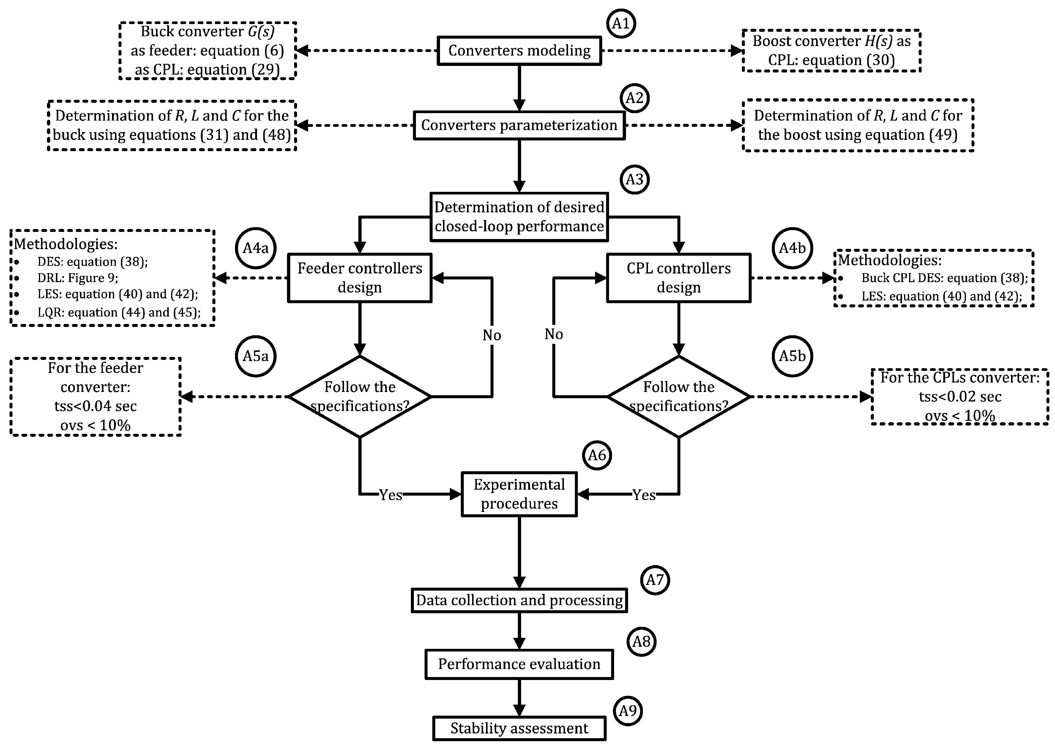
4.1. Feeder Controllers Design

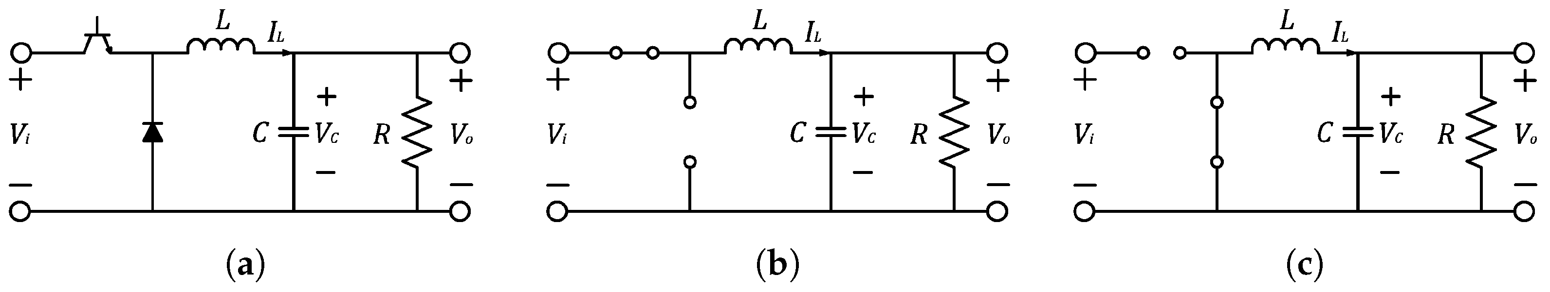
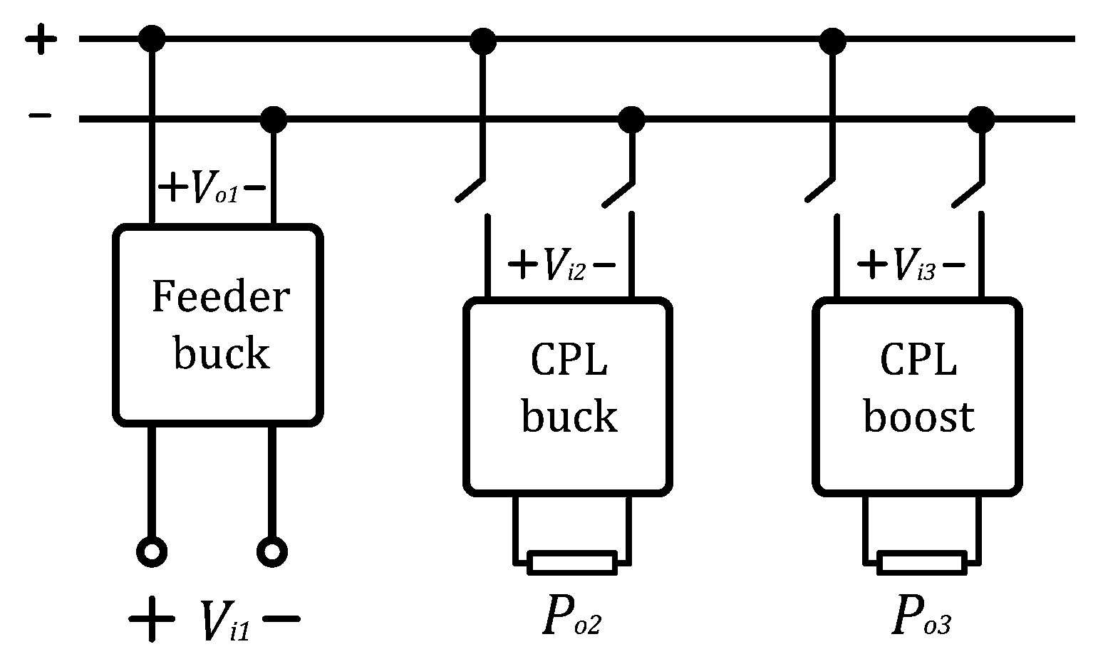
The feeder is designed from the buck converter shown in Figure 1a. The first step is to determine parameters R, L and 
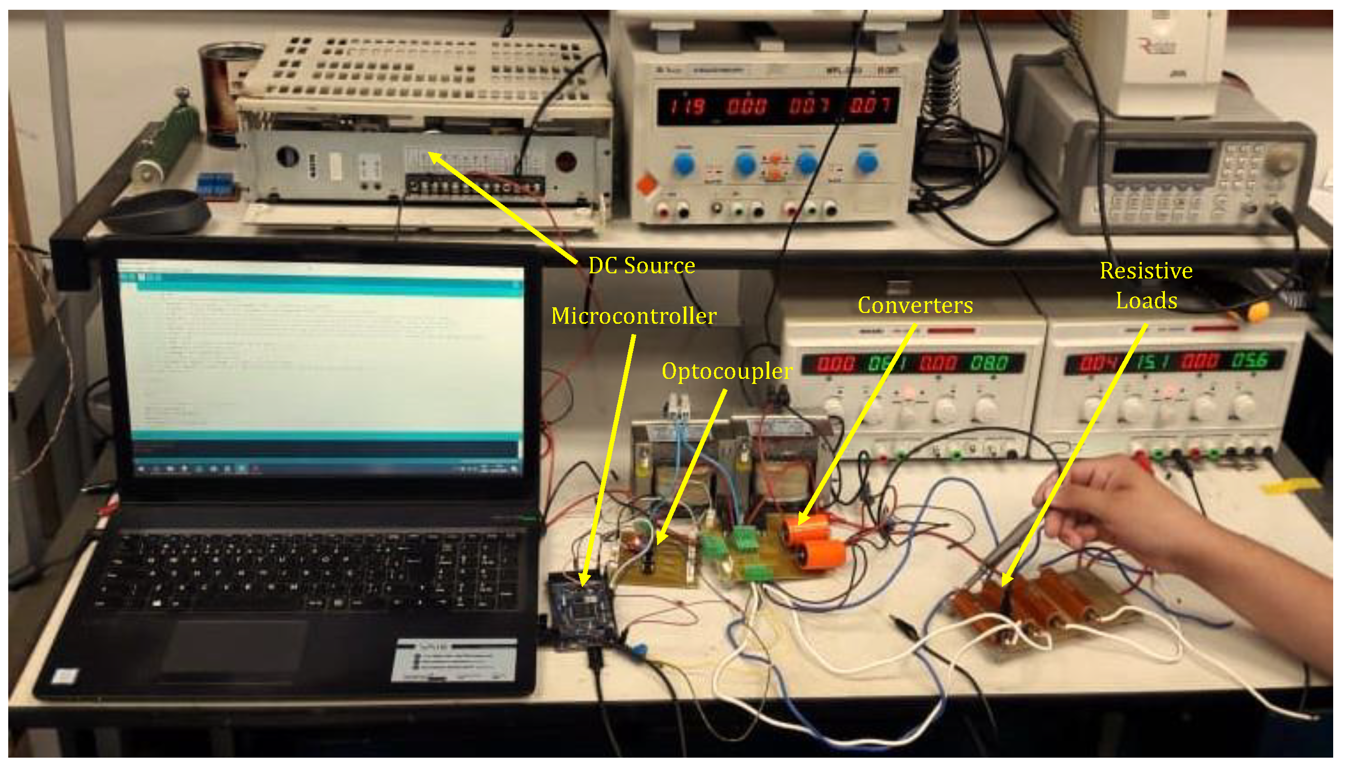
C. For this, had available a 12 V voltage source with a maximum current supply of 6 A. The buck converter regulates this voltage for the DC bus with V o = 6 V. A current ripple Δ I L in the inductor below 1 A and a voltage ripple Δ V C V C in the capacitor below 10% of the output voltage was desired. The switching frequency of 20 kHz of the converter was chosen based on the determination of the 1 mH inductor, which required a minimum frequency of 3 kHz for the CCM operation of the converter and a switching frequency below 100 kHz for correct operation of the IGBT used. Therefore, with the help of the set of equations in Equation (31), the parameters were determined as indicated in Table 1.
V o = d V i Δ I L = V o ( 1 d ) L f Δ V C V C = 1 d 8 f 2 L C
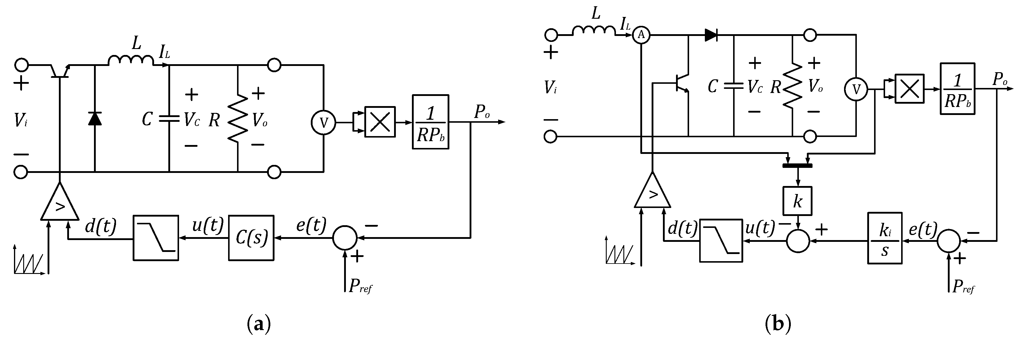
With the converter parameters determined, the next step is to design the controller that ensures system stability in addition to meeting performance specifications. In this sense, two control structures for the feeder project are addressed. The first is the output feedback shown in Figure 8a. The second structure is the state feedback shown in Figure 8b. The output feedback structure is based on determining the controller C ( s ) based on performance specification. In this paper, the controller C ( s ) is designed by using two techniques. The first is through the Diophantine equation solution (DES) and the second is using the graphical tool of the root locus (DRL). The state feedback structure is designed in order to determine the gains k and k i through the solution of the Lyapunov equation (LES) and through the solution of the Riccati’s equation for designing a linear-quadratic regulator (LQR).
The control design goal is to ensure that the converter has a settling time t s s less than 0.04 s and a maximum overshoot o v s less than 10% with the guarantee of zero error at the step. These performance specifications allows to compute the damping coefficient ζ and natural frequency ω n as follows.
o v s = 100 e ζ π 1 ζ 2 , t s s = 4.6 ζ ω n
Finally, the desired polynomial is constructed composed of an auxiliary pole p o , as follows. Notice that the gains designed depends on the chosen control structure.
Q ( s ) = ( s 2 + 2 ζ ω n s + ω n ) ( s + p o ) = s 3 + q 1 s 2 + q 2 s + q 3
The plant dynamics and the controller for the buck converter is generically described as follows.
G ( s ) = B ( s ) A ( s ) = a 0 s 2 + a 1 s + a 2
C ( s ) = N ( s ) M ( s ) = n 0 s 2 + n 1 s + n 2 s
In sequel, the closed-loop characteristic polynomial is described by Equation (36) that should be equivalent to Equation (33), resulting in the Diophantine Equations (36) and (37). The solution of Diophantine equations determines the controller gains by DES.
P c l ( s ) = A ( s ) M ( s ) + B ( s ) N ( s )
Q ( s ) = P c l ( s )
A ( s ) M ( s ) + B ( s ) N ( s ) = s 3 + q 1 s 2 + q 2 s + q 3
To ease the compute process, Equation (37) is rewritten in the matrix form, staying in the form of the Sylvester equation as indicated in Equation (38).
a 0 0 0 0 a 0 0 0 0 a 0 n 0 n 1 n 2 = q 1 b 1 q 2 b 2 q 3
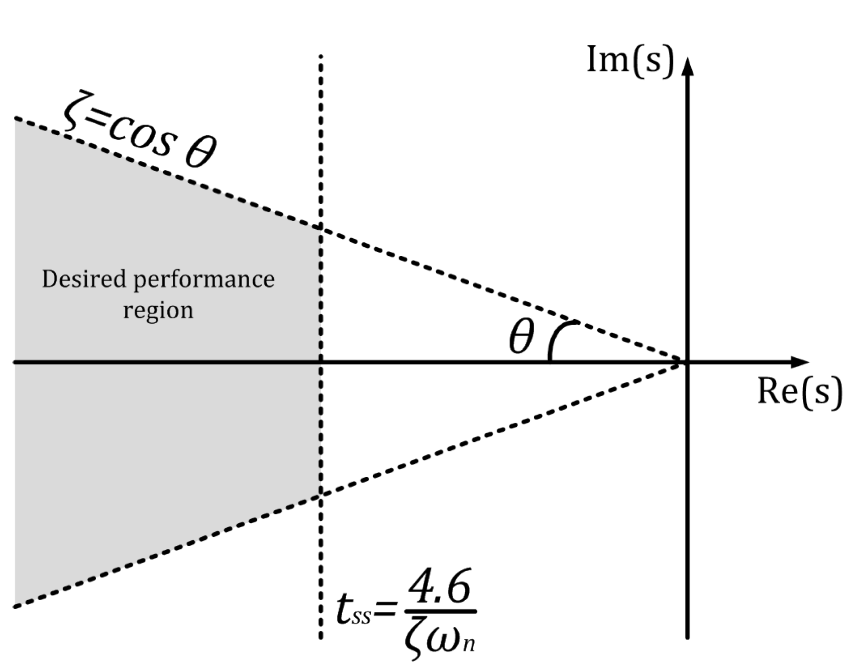
Another way to design the controller is based on the root locus, that is a graphical tool to plot the roots of the characteristic closed-loop polynomial shown in Equation (36) in s-plane. Thus, the DRL design specifies the desired performance region from a ζ and ω n as shown in Figure 9 and the gains of C ( s ) are computed to ensure that the roots are within that region.
For the state feedback structure with robust tracking, the augmented model is obtained to include the error dynamics and gains k = k 1 k 2 and k i should be computed. Therefore, the augmented model of the buck converter is described as follows
x ¯ ˙ = A ¯ G B ¯ G K x ¯ + B ¯ V V r e f
where
v = 0 t ( V r e f C x ) d t , x ¯ = x v , x = I L V C , A G = 0 1 L 1 C 1 R C , B G = V i L 0 ,
A ¯ G = A G 0 C G 0 , B ¯ G = B G 0 , C G = 0 1 , B ¯ V = 0 1 , K = k k i
thus, it is possible to compute the controller’s gains by solving the LES
A ¯ G T T F = B ¯ G K ¯
where, F R 3 × 3 is a matrix whose eigenvalues are the roots of the closed-loop characteristic polynomial and K ¯ R 1 × 3 are initial values where the set ( F , K ¯ ) is observable. In particular, the following F is chosen based on performance specifications (cf. Equation (32)) to obtain settling time and maximum overshoot lower than the specifications, since the dominant pole is real ( 1.5 ζ ω n ) and about 50 % further from the origin than the desired damped frequency circle, i.e., with radius equal to ζ ω n .
F = 4 ζ ω n 3 ω n 1 ζ 2 0 3 ω n 1 ζ 2 4 ζ ω n 0 0 0 1.5 ζ ω n , K ¯ = 1 1 1
The solution of Equation (40) determines the value of T, which allows compute the K = k k i as follows.
K = K ¯ T 1
Finally, the LQR methodology consists in optimizing the following cost function to design K:
J = t i t f ( x ( t ) Q ¯ x T ( t ) + d ( t ) R ¯ d T ( t ) ) d t
where, the matrices Q ¯ and R ¯ are gains that allow a trade-off between better performance or better control effort. Notice that Equation (43) must comply with the Lyapunov criteria described in [19,20], and the Riccati equation is derived from in Equation (44).
A ¯ G P P B ¯ G R ¯ 1 B T P + P A ¯ G = Q ¯
Considering the following matrices Q and R used to design the gains, and applying in Equation (45), it is possible to compute the gains to achieve the desired behavior established in Equations (43) and (44).
Q ¯ = 0.005 0 0 0 0.001 0 0 0 1000 , R ¯ = 5.0
K = P B R ¯ 1
Finally, the designed controllers are digitally implemented, so the controller described in Equation (35) can be expressed in digital form for a sampling period T s = 0.4 ms indicated in Equation (46) through the exact discretization of matching poles and zeros using the z = e T s s relationship.
C ( z ) = R ( z ) S ( z ) = r 0 z 2 + r 1 z + r 2 z 1
However, the integral gain in the state feedback structure was discretized by using the euler method where s = z 1 T s , therefore the integral controller is described by means in Equation (47).
C i ( z ) = R ( z ) S ( z ) = k i T s z 1
The digital controller gains for the feeder are summarized in Table 2 considering the sampling time T s = 0.4 ms. The resulting gains are presented in Table 2. Notice that the k i gain should be multiplied by the sampling time to obtain the control law to be embedded in the micro-controller.

4.2. CPL Design

After the feeder design, the next step is to design the CPLs by using the buck and boost converters. CPLs are designed to be powered by a voltage of 6V to ensure that the demanded current is within the source limitations. For the CPL buck, a current ripple Δ I L < 1 A and a voltage ripple Δ V C V C < 10 % were considered. A V i = 6 V supply with a switching frequency f = 20 kHz. For a duty cycle base d b = 1 , the output power is specified for P o = 0.3 p.u. by means of Equation (48).
P o = ( d d b ) 2 Δ I L = V o ( 1 d ) L f Δ V C V C = 1 d 8 f 2 L C
Whereas, for the CPL boost, a current ripple Δ I L < 1 A and a voltage ripple Δ V C V C < 10 % is considered and V i = 6 V supply with a switching frequency f = 20 kHz. For a duty cycle base d b = 4 2 4 , the output power was specified for P o = 0.3 p.u., then through the set of equations in Equation (49).
P o = ( 1 d b 1 d ) 2 Δ I L = d V i L f Δ V C V C = d f R C
The parameters of the designed CPL converters are summarized in Table 3. Finally, the controller gains to ensure the CPL operation of converters are computed. The buck converter is designed by using output feedback structure and the boost converter is designed by using the robust tracking state feedback structure as shown, respectively, in Figure 7a,b. The design specifications are t s s < 0.02 s and o v s < 10 % to ensure that the CPL dynamics is faster than the feeder dynamics.
The CPL buck design is carried out from DES in the same way as indicated in the previous Section 4.1. The CPL boost design is carried out through LES. The gains of CPL controllers are summarized in Table 4, considering the discretization with sampling period T s = 0.2 ms.
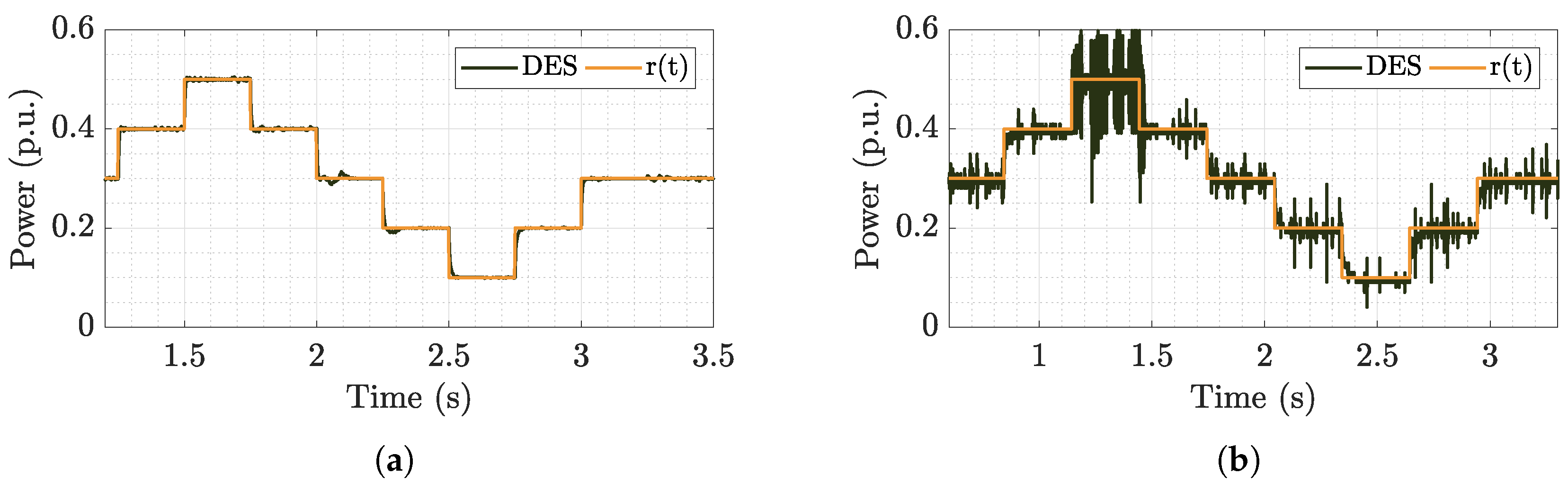
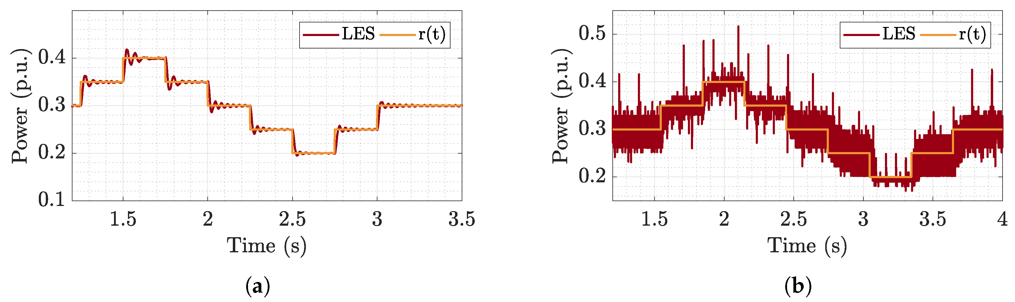
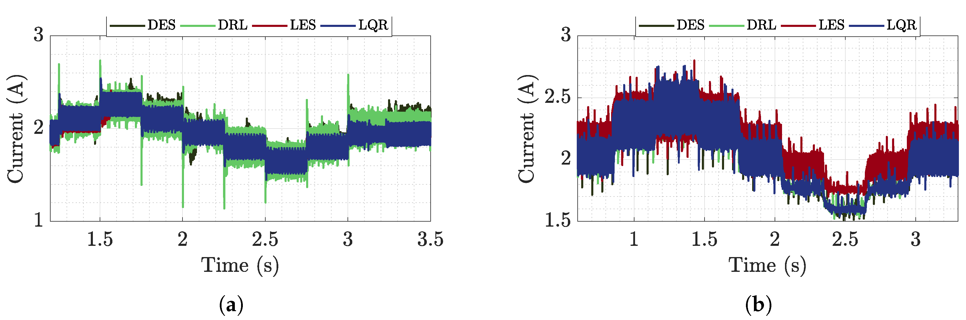
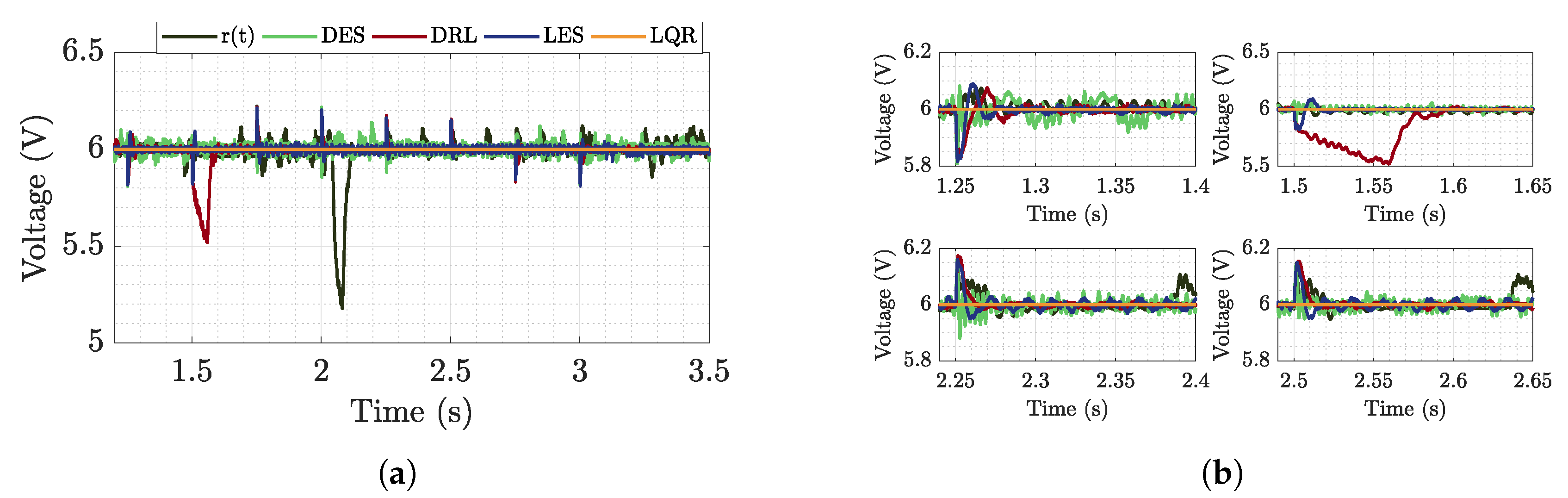
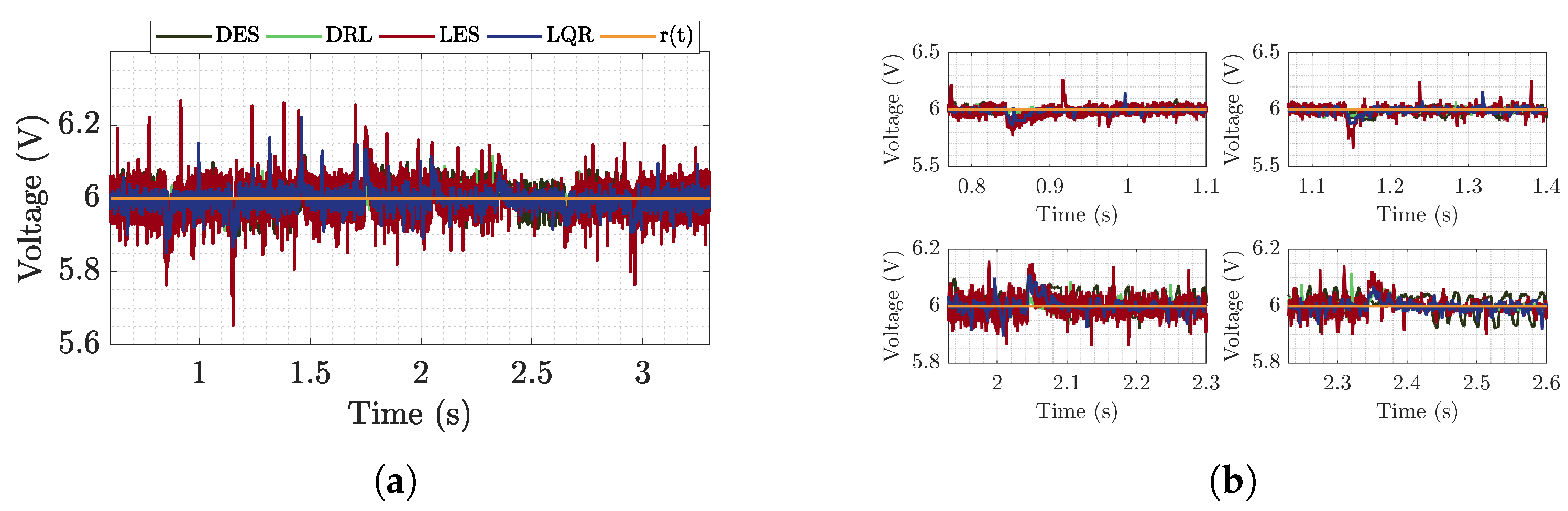
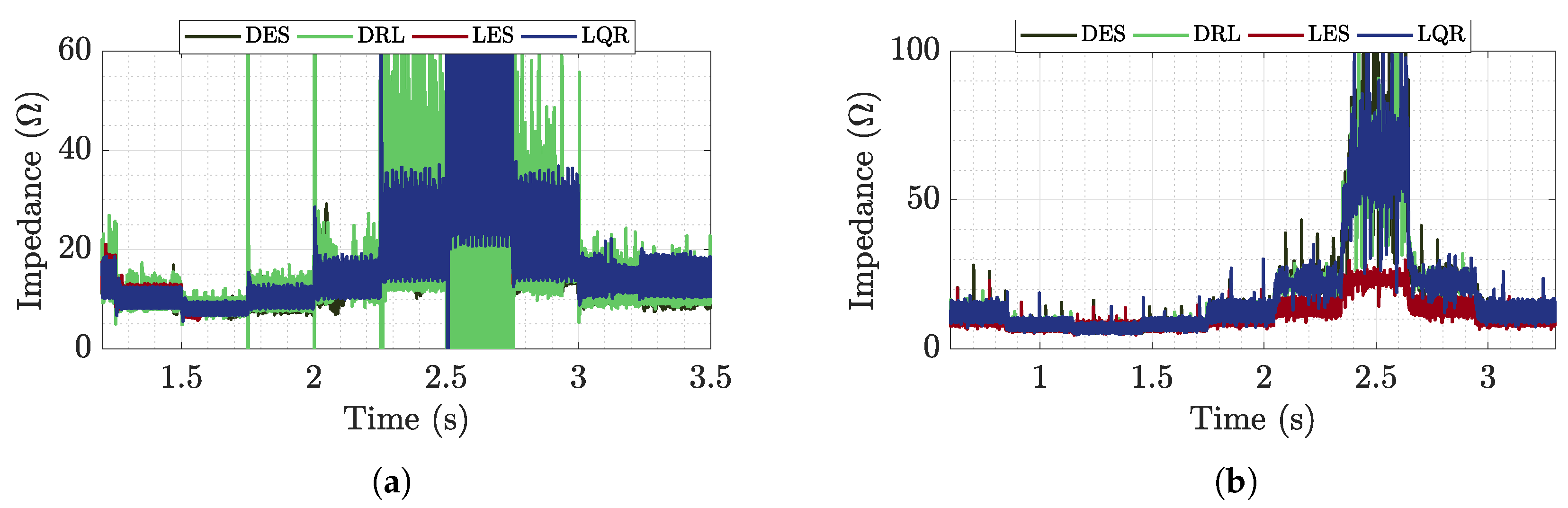
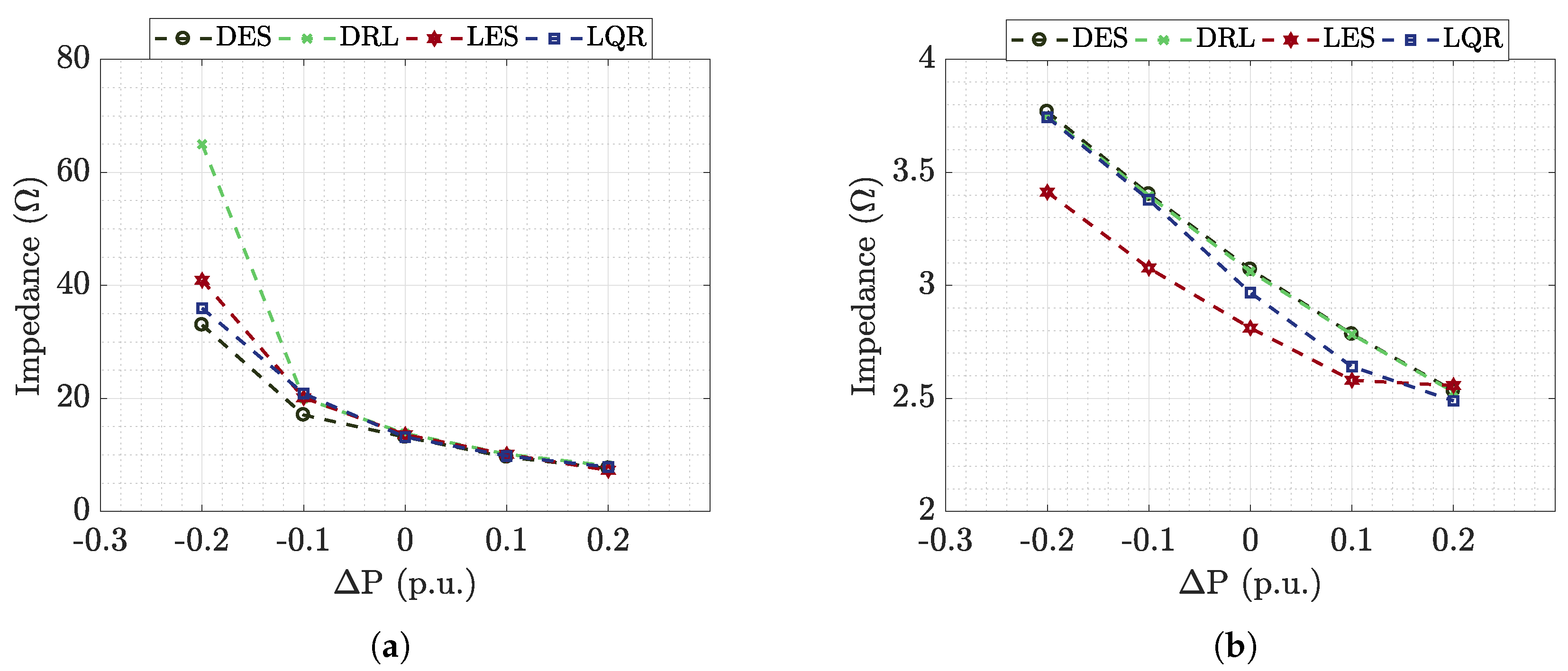
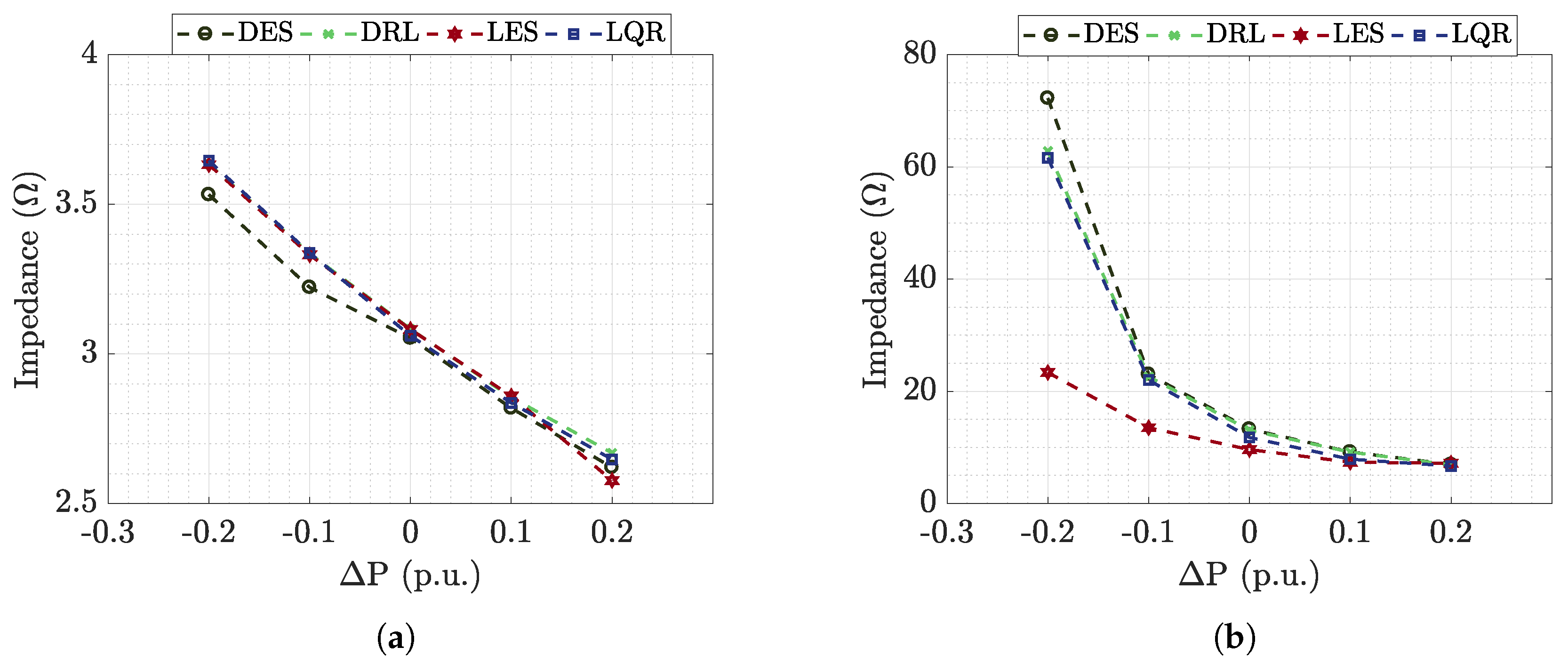
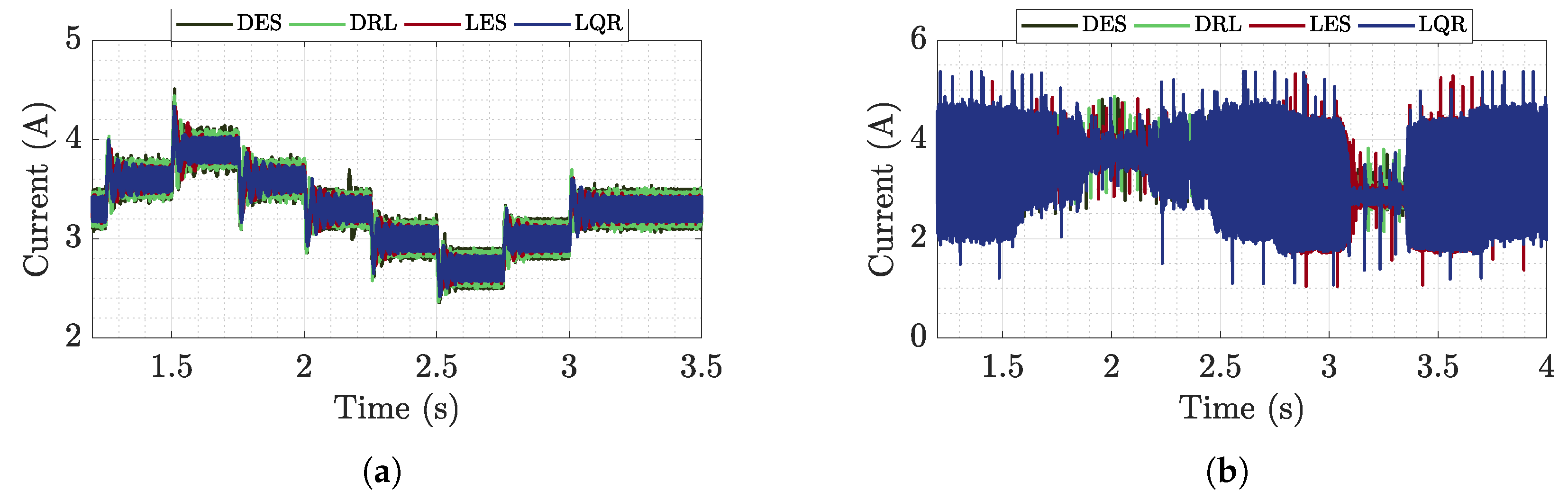
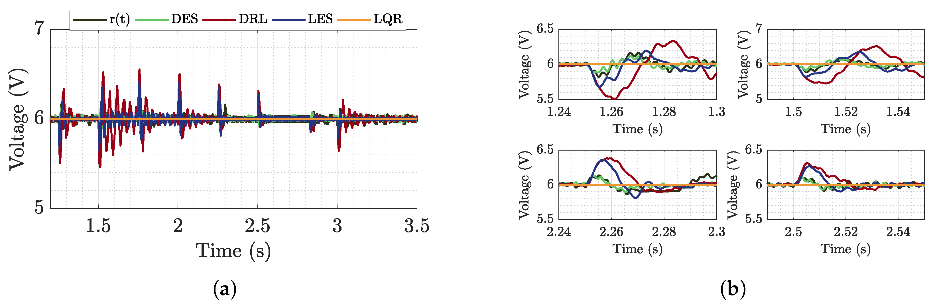
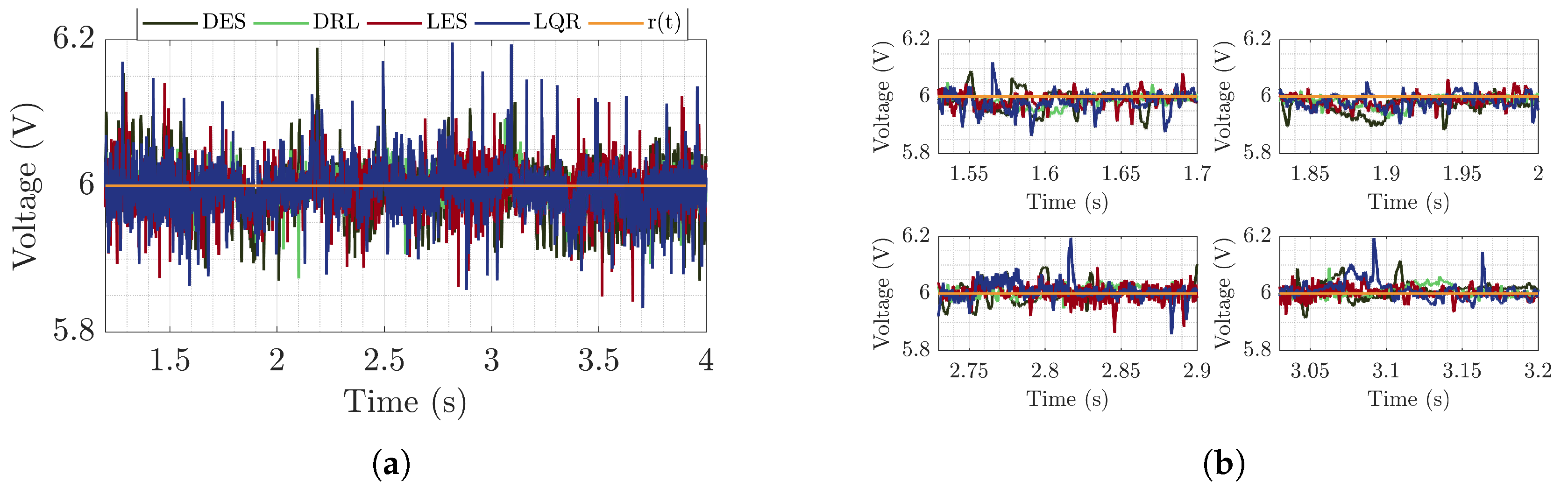
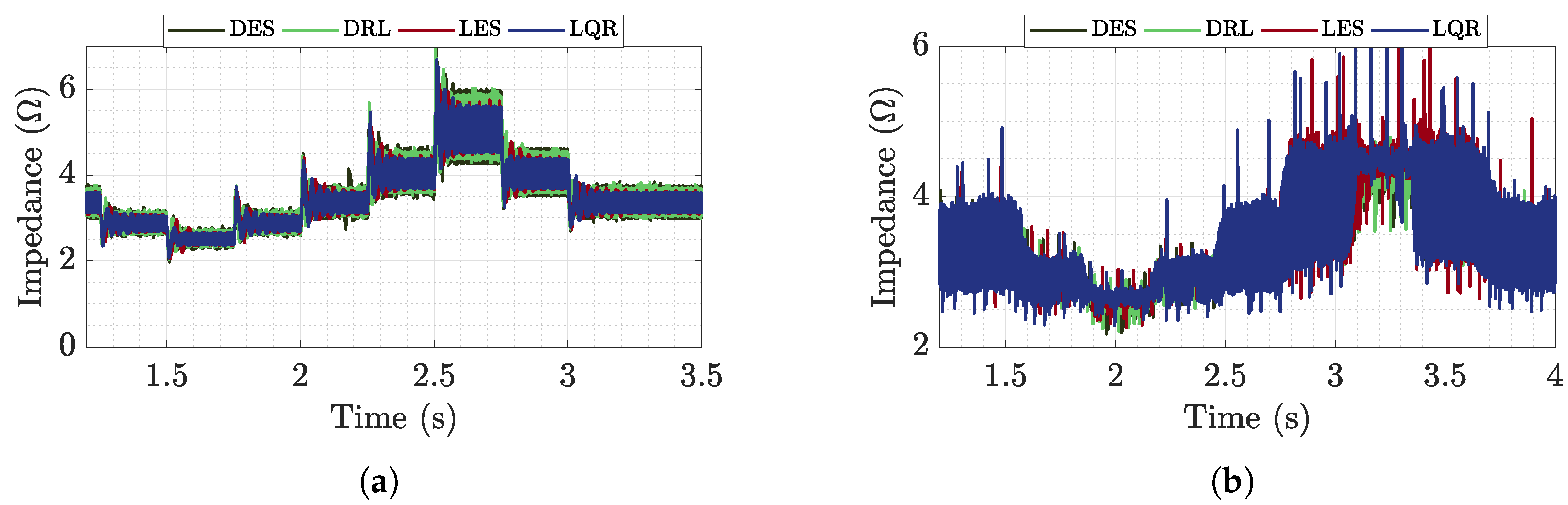
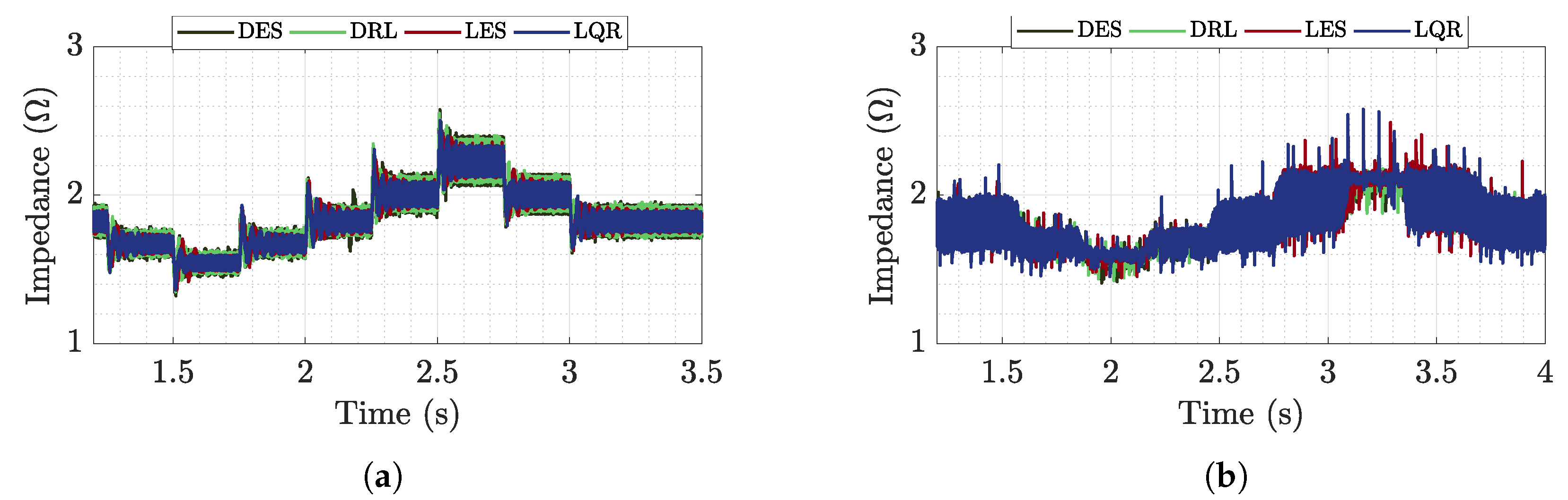
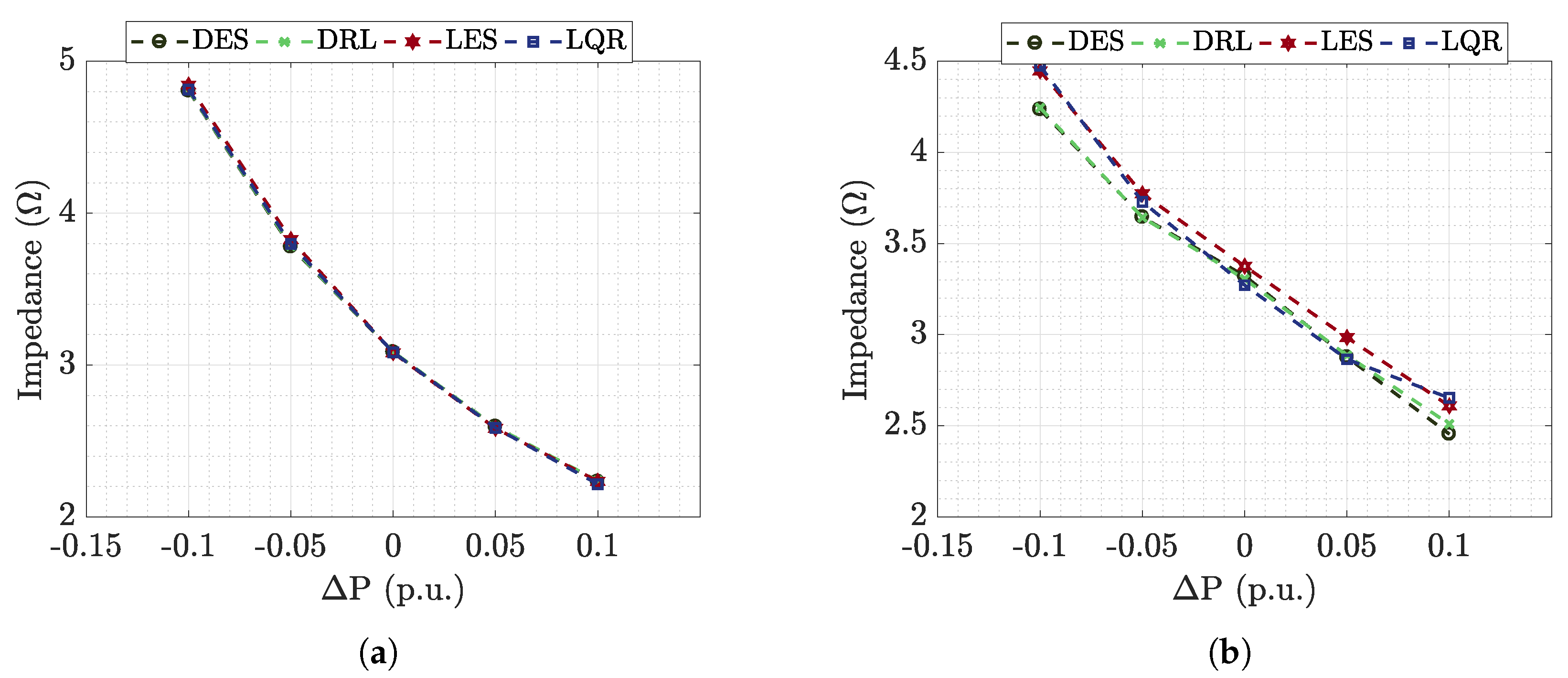
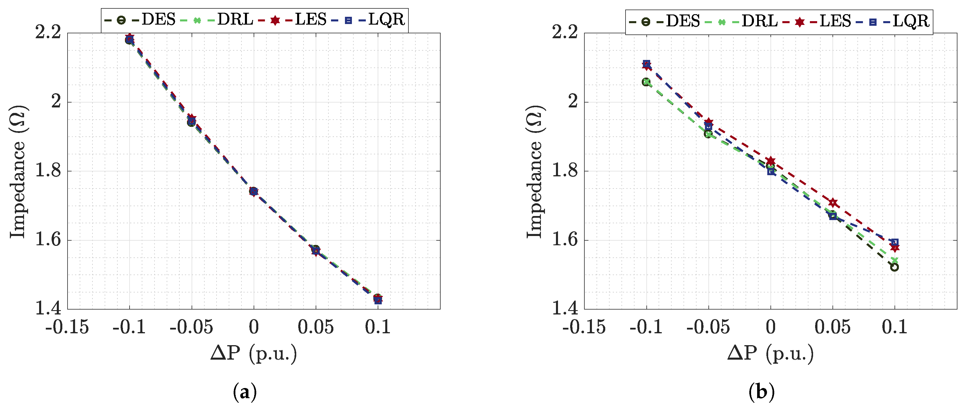
The validation of the CPL buck is shown in 
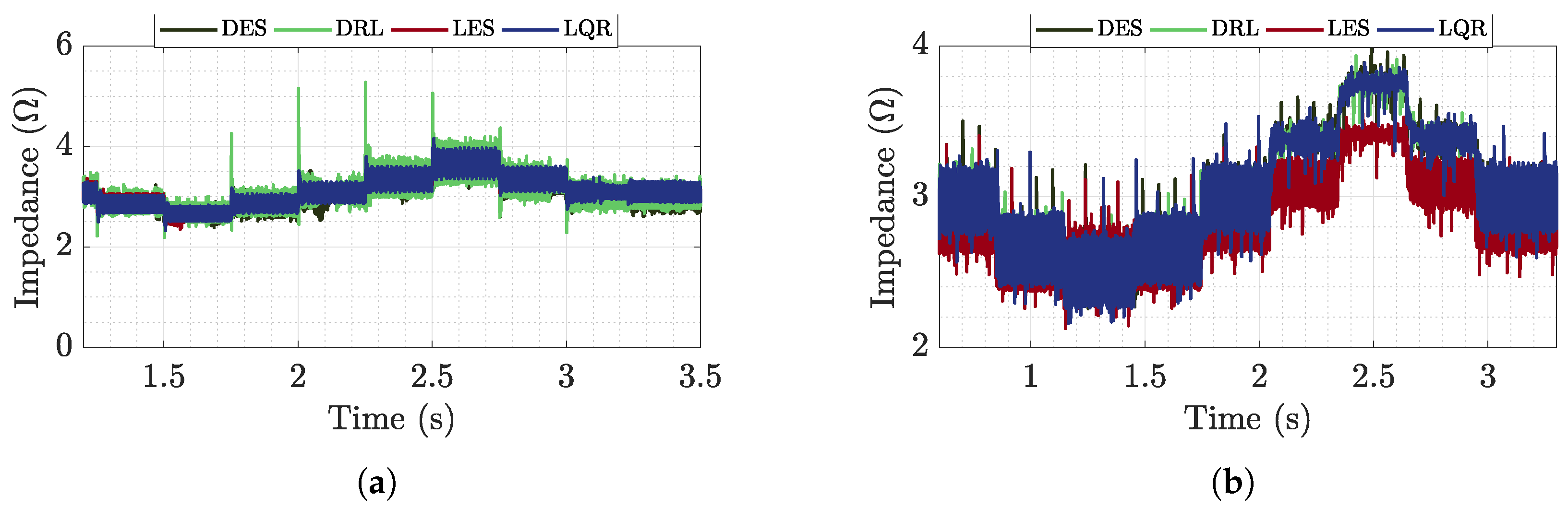
Figure 10, while the validation of the CPL boost is shown in 
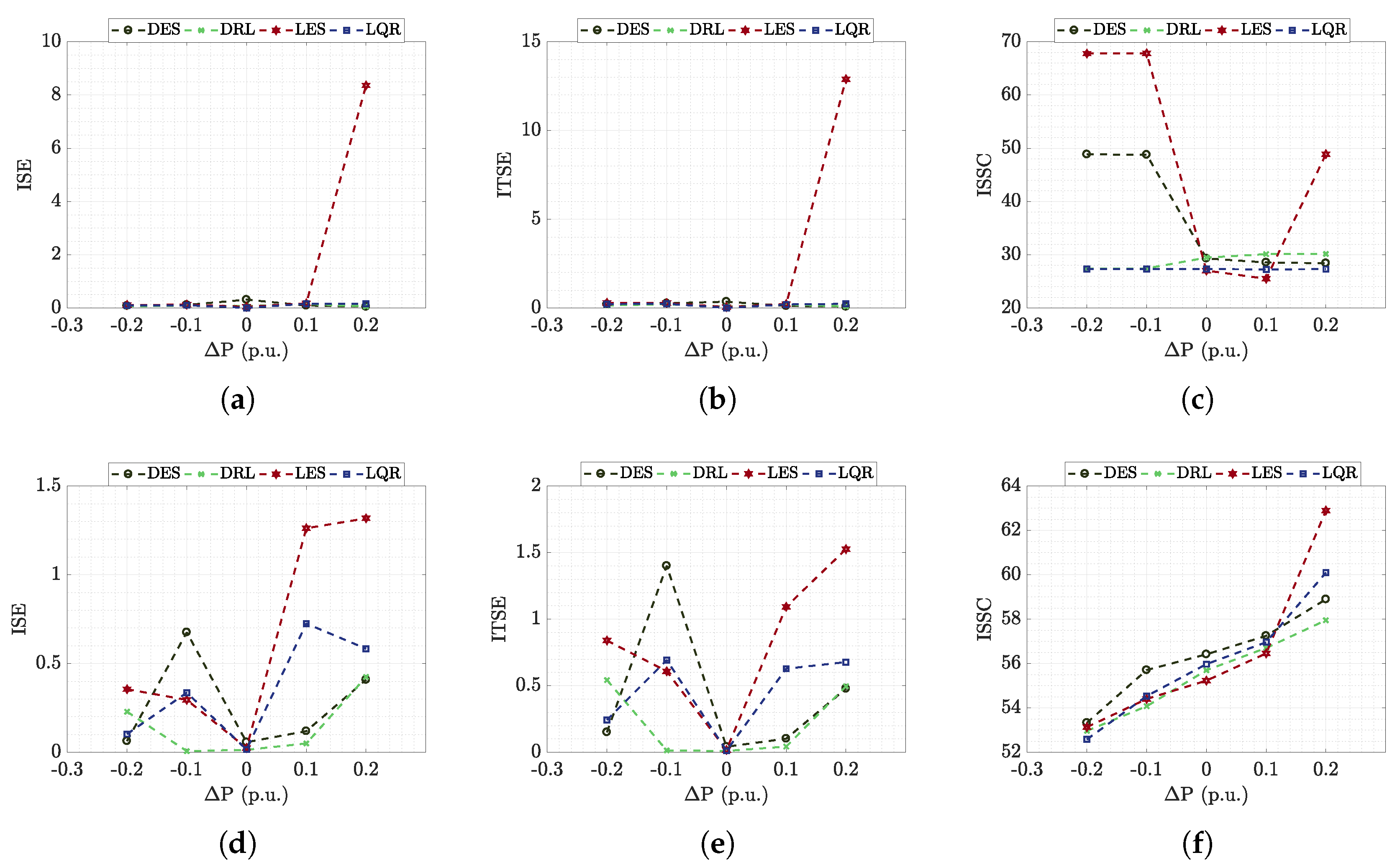
Figure 11 connected to the DC bus fed by the feeder, for each proposed methodology.
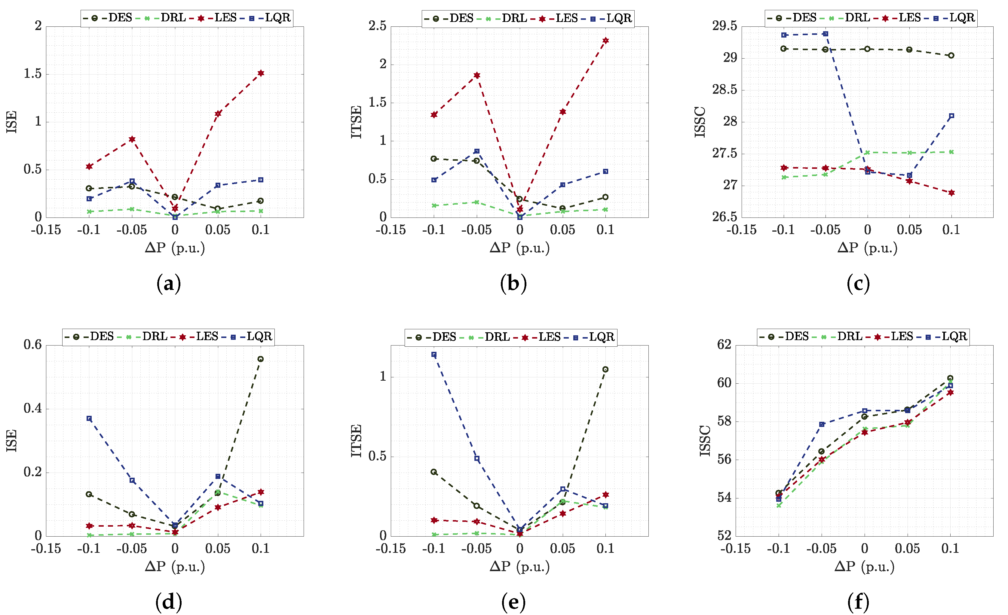
In both situations, the CPLs are validated by simulations and tests. The power variation applied to the boost converter is less than that of the buck converter due to the greater complexity of the boost converter (i.e., non-minimum-phase dynamics due to zero in the right semi-plane), which provides a higher current variation than the buck converter. The results indicate that both converters are able to operate as CPL, since the proposed performance requirements are met.

5. Methodological Procedures

This paper proposes to compare the performance and stability of the DC microgrids when the control techniques presented in Section 4 are implemented for both feeder and CPL converters. For this purpose, the methodological procedures adopted in that comparative investigation are presented in Figure 12. The implementation of the microgrid is carried out from steps A1 to A5 of the flowchart, while step A6 is described by the test environment, in addition the data treatment is presented from steps A7 to A9.

5.1. Proposed Microgrids

The use of renewable energy sources enables the growth in cascade converters usage, as shown in Figure 13 that represents the proposed microgrid, where the feeder can be connected to a CPL buck or CPL boost. The isolated operation of the microgrid is common in electric vehicles, shipboards, aircraft and submarines, as they contain the main DC bus supplying several loads [32]. The power converters (buck or boost) used to regulate these loads are designed to operate as CPL.
This work implements two microgrids topologies, buck-buck and buck-boost, to evaluate the performance of the voltage regulation provided by the buck feeder when connected both CPL. From the chosen microgrid, the state variables, i.e., the currents in the inductor and voltage in the capacitor, of the used converters are acquired. The other variables of interest are generated from the state variables.

Microgrid Implementation

According to the flowchart in Figure 12, step A1 consists of the modeling of the power converters, using the ASM and the linearization around the OP, as indicated in Equations (6), (29) and (30). In step A2, the constructive parameters of the converters are obtained based on static equations described in Equations (31), (48) and (49). The desired closed-loop polynomial based on the designer’s specifications is built in step A3. These specifications are set to ensure that CPL has a faster dynamic than the feeder aiming to allow the CPL-like behavior during the instantaneous power variation.
In step A4 the controllers are designed. In step A4a, the feeder controller gains are computed based on two control structures; output feedback and state feedback. The output feedback structures are designed by using DES (cf. Equation (38)), and DRL based on a performance region shown in Figure 9. For the state feedback structure, the gains are designed by using LES based on the solution of Equation (40), and LQR using the solution of Equation (44). In step A4b, the CPL controllers are designed. For the CPL buck the DES methodology is used, while for the CPL boost, LES is used. Finally, step A5 consists of assessing whether the controllers designed in steps A4a and A4b followed the design specifications.

5.2. Experimental Procedures and Test Environment Description

The steps A6 to A9 in the flowchart of Figure 12 are related to the performance of the proposed experiments of power variation for the evaluation of stability and performance of the microgrid. The experimental procedures are started in step A6, through the integration of the microgrid and the performance of the power variation test. The simulation is implemented in the MATLAB. In particular, the simulation of the proposed microgrid is carried out in Simulink/Powergui tool using fixed step of 10 6 s during a time of 3.5 s. The test environment is the test bench shown in Figure 14.
The converters are switched through a set of optocouplers consisting of the HCPL 3120 chip that allows the electronic circuit to be separated from the power circuit. The static switch used is the IGBT IKW75N60T in conjunction with diode 30CPH03. The measurement of the capacitor voltage and inductor current is carried out through the voltage meter module and the ACS712 current sensor module. The collected information is sent to microcontroller Atmel SAM3X8E ARM Cortex-M3 CPU where in its interface the implementation of digital controllers is performed to carry out the regulation of the microgrid. The control signal is sent to the optocoupler circuit that will activate the static switch.
The procedure for operating the microgrids is shown in the flowchart in Figure 15. Step B1 is to connect the buck converter that will operate as the feeder to the main power source. This converter is placed in the OP and then, in step B2, it is placed in closed loop, choosing one of the projected methodologies. With the closed loop converter and the POL, the CPL is connected to the system.
In the step B3, the CPL buck (step B3a) or the CPL boost (step B3b) is connected to a static switch that is initially turned off. Finally, the converters are placed in closed loop in step B4, making them operate as CPL. For the buck converter, the output feedback structure is adopted, while for the boost converter the state feedback structure is used.
With the CPL in the POL, the microgrid is implemented, and the reference variation test is carried out in step B5. When the CPL buck is connected to the feeder, the POL occurs for P o 2 = 0.30 p.u. Thus, the power variation occurs in + 0.10 p.u. until it reaches 0.50 p.u. when it returns to the POL. Then there is a negative variation of 0.10 p.u. until it reaches 0.10 p.u., returning to the POL. On the other hand, when the CPL boost is connected to the feeder, the POL occurs for P o 3 = 0.30 p.u. Thus, the power variation occurs in + 0.05 p.u. until it reaches 0.40 p.u. when it returns to the POL. Then there is a negative variation of 0.05 p.u. until it reaches 0.20 p.u., returning to the POL.
The variation of the power reference of the CPLs allows to observe the behavior of the voltage delivered to the DC bus at each instant of variation. Another point to be noticed is the level of current flowing through the feeder inductor, which is essential for determining the impedances used for estimating the stability margin of each proposed microgrid. It is worth mentioning that the increased load demand causes an increase in the current ripple in the inductor, which can result in two critical scenarios:
  • It leads the system to discontinuous conduction mode (DCM) causing the system collapse, since the controllers are not designed to deal with DCM.
  • It modifies the feeder OP, losing the DC bus voltage regulation ability.

5.3. Data Processing

Finally, the step A7 in Figure 12 consists of the data acquisition during the experiments. The state variables are collected from the power converters. In addition, the control signal applied to the static key and reference gate is observed and the error signal is calculated externally. In step A8, the performance evaluation of the proposed microgrids using figures of merits and the stability analysis of the microgrids is carried out in step A9 through the evaluation of CPL input impedance.
With the acquired data, the data treatment flow is shown in Figure 16. The processing step C1 is to set the power variation intervals in a simulated and experimental test, analyzing from the moment when the variation occurs until the moment when the DC bus voltage returns to the reference value. Then, (cf. presented in step C2 of the Figure 16), the inductor current and output voltage are acquired for calculating the impedance, control signal, reference value of the voltage and tracking error used for performance evaluation.
Then, the performance indices are calculated in parallel with the determination of the systems impedances. These steps are described below.

5.3.1. Perfomance Evaluation

In the data processing flowchart depicted in Figure 16, step C3 regards to compute the performance indices. Since the feeder operates in closed loop, the tests are performed connecting the CPL and made the power variation of the CPL aiming to investigate the behavior in DC bus (i.e., feeder’s voltage output). The acquired data obtained by means of the experiments are processed for the evaluation of the controllers’ performance. In this sensors, three performance indices are adopted as described in [33].
The indices used in this work are: the integral of squared error (ISE) which aims to evaluate accumulated error during the experiment; the integral of time-weighted squared error (ITSE) which aims to evaluate the speed of the error mitigation; and the integral of squared signal of control (ISSC) that evaluates the demanded control effort. These indices are defined as follows.
I S E = e 2 ( t ) d t , I T S E = t e 2 ( t ) d t I S S C = u 2 ( t ) d t
The indices are computed for each power variation stage and with that it is possible to carry out the performance evaluation of each controller proposed for each microgrid topology (cf. presented in step C4 of the Figure 16). The higher ISE values for a methodology indicate higher accumulated error and worse oscillation mitigation. Thus, when the converter is operating in the OP and with the CPL in POL, it is expected an error signal with approximately zero expected value. In addition, higher ITSE values indicate a slower response and oscillation mitigation, since that index is weighted by time. Finally, higher ISSC values indicate greater control efforts for ensuring voltage regulation on DC bus.

5.3.2. Stability Assessment

The right side of the flowchart in Figure 16 regards the system stability assessment. With the current and voltage data from the feeder, considering I C 0 , the time series of the CPL input impedance Z C P L is computed (step C5) as follows
Z C P L ( t ) = V C P L ( t ) I C P L ( t ) ,
V C P L = V C 1 , I C P L = I L 1 V C 1 R 1 .
In addition, the Z C P L depends only on the parameters of the feeder because the CPL design ensures a dynamics much faster than the feeder dynamics that become dominant for the microgrid dynamics. Thus, the time series of the feeder output impedance is computed as Equation (53).
Z F ( t ) = V C 1 ( t ) I L 1 ( t )
Thus, considering that for each variation interval n C P L and n F , it is possible to estimate the average input and output impedances (step C6) for each power variation and the minor loop gain T o to assess the stability of each methodology proposed in each microgrid (step C7).
Z ¯ C P L = Z C P L n C P L Z ¯ F = Z F n F
| T o | = Z ¯ F Z ¯ C P L
Finally, in step C8, the stability of each methodology is analyzed for each microgrid based on the Middlebrook criteria presented in Section 3 so that the higher the | T o | , the lower the overall stability of the system. Thus, the increase in load should imply in less stability for all proposed methodologies.

6. Results and Discussions

This section presents the results of simulations and tests. Furthermore, it is performed performance and stability analysis of the different feeder control strategies.

6.1. Buck-Buck Microgrid Analysis

6.1.1. Time Analysis

The first microgrid structure to be observed is the buck-buck which has a feeder implemented by a buck converter and a CPL operated from a buck converter. The CPL power variation test is performed in the system as shown in Figure 10. Figure 10a shows the output power of the CPL buck during the simulation while Figure 10b presented the output power during the test.
The current observed in the simulation (cf. Figure 17a) has a smaller current ripple than that observed in a test (cf. Figure 17b). In both cases, the system operates in CCM, ensuring the best operation of the controllers.
Figure 18a and Figure 19a show the regulation of the DC bus in both simulation and test environments, besides that Figure 18b and Figure 19b shows a zoom in each voltage oscillation caused by CPL power variation. However, it is possible to see the instability that a CPL causes in a DC bus in Figure 18b (for simulation) and Figure 19b (for test) where the increase in load demand causes an initial voltage reduction, while the load reduction causes an increase in voltage that is adjusted to the reference value due to the action of the proposed regulators. In addition, the largest voltage ripples are observed in experimental test, as shown in Figure 18a, for the LES approach.

6.1.2. Performance Analysis

In this section, the performance of the control strategies is evaluated by means of the performanceindices. Figure 20a–c, present the performance indices for the simulation buck-buck microgrid, and Figure 20d–f, present the performance indices for the tests.
In the simulation, the ISE and ITSE for the four methodologies are similar for most of the experiment, reflecting the same ability to mitigate oscillation in addition to similar response speed. However, for the variation of + 0.2 p.u., the LES methodology exhibits higher ISE and ITSE values as indicated by the voltage regulation response depicted in Figure 18b, where there is a large voltage dip and a greater slowdown to mitigate this effect.
Regarding the simulated ISSC depicted in Figure 20c, the LQR controller presented the most constant and lowest indices for most of the variations. It occurs due to the control design focusing on optmizing the control effort. The LES controller exhibits the higher index for negative variations and for the variation of +0.2 p.u., followed by the DES controller.
Otherwise, the ISE and ITSE indices depicted in Figure 20d,e for the test showed greater variation between methodologies. However, for positive variations, the state feedback controllers showed higher indices. It occurs because these controllers presented greater current ripple, causing a greater voltage ripple, making the oscillation mitigation smaller and slower. The DRL controller, as in the simulation, is the methodology with the most regular index, indicating a similar mitigation capacity and speed for the variation stages.
Regarding to ISSC depicted in Figure 20f, all the methodologies presented similar behaviors, with indices reduction when there is load reduction and the consequent increasing otherwise. However, for positive power variations, the state feedback methodologies exhibit greater indices increase.
Thus, in general, for both simulations and tests, the DRL methodology showed a better effort/performance ratio. On the other hand, the LES controller showed the worst performance in both environments, especially for positive variations in power. In addition, the degradation of the LQR controller is noticeable during the test. It occurs due to the greater current ripple encountered during the experiment, and as the LQR controller uses a state feedback structure, the value of the inductor current is important to ensure the correct operation of this methodology.

6.1.3. Stability Analysis

This section performs an stability analysis of the buck-buck microgrids using the calculated impedance curves. The input impedance of the CPL buck in the simulation is shown in Figure 21. While Figure 22 shows the output impedance of the buck feeder for the microgrid buck-buck.
The current required by the CPL buck is naturally lower than the current supplied by the feeder, since the feeder is responsible for supplying energy to its resistive load and to the CPL. Thus, the output impedance of the feeder is consequently lower than the input impedance of the CPL.
When the CPL requires less current from the feeder, the impedance increases. Otherwise, there is an impedance reduction for positive power variations due to a higher load demand.
In the time interval with the highest level of input impedance (cf. Figure 21) and output impedance (cf. Figure 22), it is noticed a greater ripple in the response of Figure 22. It occurs because the CPL is displaced from its OP during the power variation that coincides with highest impedance interval. During this time, the converter operation is near of discontinuous conduction mode that is the main reason of the increasing of the current ripples and the consequent increasing of the impedance.
For a better analysis, we have the CPL buck input impedance curve for each methodology obtained in the simulation (cf. presented in Figure 23a) and for a experimental test (cf. presented in Figure 23b), as well as the mean impedance of feeder output for simulation (cf. presented in Figure 24a) and practical (cf. presented in Figure 24b) during each power variation.
For the input impedance of the CPL buck during the simulation depicted in Figure 23a, the DRL and LES methodologies are observed with the highest impedance value for negative variations. For positive variations, all methodologies present similar impedance decreasing. In test environment, whose results are presented in Figure 23b, the LES controller exhibits the lowest impedance for the 0.2 p.u. variation while the methodologies with output feedback structure have the highest output impedance value. All methodologies have similar impedance.
The results of the output impedance for the feeder in a simulation are presented in Figure 24a. All methods present similar values in each variation stage. However, during the test, there is a lower impedance level of the LES methodology than the others.
Given the impedance curves for each instant of variation, we have Table 5 that indicates the minor loop gain for each variation.
It is observed that the increase in load causes an increase in | T o | , showing that the stability of the system is reduced with the increase in load. In addition, another reflection of the variation of 0.2 p.u. on the LES controller, where there is a higher value of | T o | at that moment. We also have that in terms of mean minor loop for the simulation, the DES methodology presented a lower stability margin during the test while the DRL methodology showed a higher stability margin, corroborating with its better performance observed in the previous section.
During the test, the worst performance of the LES methodology is also observed in the stability margin, presenting a greater | T o | in all variations, resulting in a mean minor loop superior to the other methodologies, as well as the degradation of the LQR controller, which presented the highest | T o | for the 0.2 p.u. variation, and again, this greater instability is related to the greater current ripple in a test environment.

6.2. Buck-Boost Microgrid Analysis

6.2.1. Time Analysis

Figure 11 shows the boost converter responses for the power variation during the simulation (Figure 11a) and test (Figure 11b). The boost converter dynamics is more complex than the buck converter due to its non-minimum-phase characteristic, in addition the connection of the converter to the DC bus already results in a current consumption (changing the OP of the feeder) even with zero duty cycle. It causes greater voltage and current ripple during the test when compared to simulation due to the higher degree of non-linearity presented in this system.
Figure 25 shows the current in the feeder inductor during the power variation test. During the simulation, shown in Figure 25a, the current levels occurred within the projected, however, during the test a high current ripple is obtained. Figure 26 and Figure 27 show the voltage level on the DC bus regulated by the feeder buck during the simulation and experimental test. Figure 26a shows the feeder’s regulation ability in the simulation with the effect of the power variation on the DC bus shown in Figure 26b. Thus, it is shown that when the boost CPL is used, there are more oscillations during power variation steps, although the controllers are still able to mitigate this effect.
Likewise, during the test, the controllers are able to mitigate oscillations by adequately regulating the voltage delivered to the DC bus, as shown in Figure 27a. However, looking at each variation window shown in Figure 27b, there are poorer mitigation performance and more oscillations. Anyway, the effect of a CPL using the boost converter is less noticeable, this can be due to two facts:
  • The boost converter causes greater voltage and current ripples in the system, thus the regulatory effect of CPL converter is spoiled;
  • The boost converter dynamics during the test, for the same gains, is distinct from the simulation when it is connected to the DC bus due non-linearities found in a test, thus it is noticed that the effect of a CPL is better observed when the converter power regulation performance is closer to instantaneous, also indicating that the design of a fast feeder can help mitigate the effect of CPL.

6.2.2. Performance Analysis

The next step is the performance analysis by means of the performance indices depicted in Figure 28a–c for simulations an in Figure 28d–f for practical tests.
For the simulation it is observed that the LES approach had a higher ISE and ITSE during power variations. In general, the increase in power variation caused an increase in ISE and ITSE for all methodologies. Thus, the LES approach presents the greatest accumulation of error while the DRL controller presents the least amount of error in the oscillation mitigation.
During the test, LQR approach presents the highest ISE and ITSE indices for all power variations and in the OP. An important observation is made for the variation of + 0.1 p.u., where the DRL approach has a peak of ISE and ITSE, resulting in a point of greater accumulation, in other words that indicates the slow in correction of the oscillation causing more accumulated error.
The ISSC during the simulation, shown in Figure 28c, indicates the LES and LQR controller with the lowest ISSC at the point of operation. The controllers showed approximately constant rates for all the variations made where the DES controller presented the highest ISSC for all the power variations, being the methodology with the greatest control effort in mitigating oscillations in a simulated environment.
For the test, all methodologies presented similar ISSC, with the index increase for positive variations and index decrease for negative variations. The LQR controller exhibits the highest ISSC in the OP. For positive variation, the DRL controller exhibits the highest index. Thus, in the OP, the LQR control has a greater control effort, while far from the operating point the DES controller presents a greater control effort. Thus, through the analysis of the PI, a large discrepancy is observed between the simulated and practical data obtained during the experiment for the CPL boost.

6.2.3. Stability Analysis

The CPL boost current is initially higher than that of the CPL buck, resulting in a system with lower input impedance in comparison with the buck-buck system, as depicted in Figure 29, which is also reflected in a lower feeder output impedance, as shown in Figure 30.
For the sake of simplicity, the average input impedance value is computed for CPL and it is depicted in Figure 31a for simulations and in Figure 31b for the tests. The average output impedance is shown in Figure 32a for the simulations and in Figure 32b for tests.
All methodologies exhibit similar output impedance for the CPL boost in the simulation. During the test, the DES and DRL methodologies presented an impedance value slightly lower than the other methodologies. The output impedance of the feeder connected to CPL boost is shown in Figure 30a during the simulation, where it is observed that all methodologies presented similar mean impedance. During the test (cf. presented in Figure 30b) the DRL methodology presents a lower level for each variation. Notice that the CPL input impedance for each instant of variation is less than the impedance of the CPL buck presented in the previous section, as well as the output impedance of the feeder. The lower impedance is reflected in the minor loop gain calculated for the boost converter and shown in Table 6.
It is observed that the boost converter connected to the feeder as CPL imposed on the system a current consumption higher than that of CPL buck, where in the POL of CPL boost, the minor loop gain is at least twice higher than the POL point of CPL buck, justifying a greater instability observed during the test is in the form of a greater current ripple. In addition, the lower load demand of the CPL boost (occurring to 0.1 p.u.) has a minor loop gain higher than the greater load demand of the CPL buck, which indicates that the designed CPL boost is a more complex plant due to its non-minimum-phase characteristic and its higher current consumption. Thus, the connection of CPL boost took the feeder to an OP far from the project, although all methodologies are able to guarantee the stability of the system, even for a much higher load level, although it is reflected in a worse performance of the controllers, especially those that uses the current state to carry out the control. Finally, it is observed the buck-boost microgrid presents an increase in the current level consumed by the CPL, resulting in less stability, making it closer to the threshold of the Middlebrook criterion.

7. Conclusions

This paper examined the enhancing stability when the DC-DC converter system feeds another DC-DC converter that operates like a CPL. Since the converters are usually cascade connected the CPL behavior causes unwanted oscillations that might evolve to instability in DC bus. This paper proposed ways to enhance the stability margin of the DC microgrid by using control techniques applied on the feeder converter, besides that it performed a comparative analysis of the control techniques investigated, however to guarantee the CPL behavior a strictly control technique must be implemented in the load converter to behavior as CPL.
The stability margin is improved when the system uses control techniques in both microgrids topologies, also that the second topology (i.e., buck-boost converter) presented a greater instability in comparison the first, this situation occurred due to the boost converter operating like a CPL presented a greater current ripple than other microgrid degenerating the performance and causing worst behavior to this topology. The validity of this comparative study to enhance the stability margin of the DC microgrid was ratified by the simulations and the experiments using the two topologies, i.e., buck-buck converters and buck-boost converters. This discussion reveals that although the CPL behavior, the microgrid can maintain the stability using control techniques and improve the performance of the system. The tests indicated that the classical methods based on the feedback output outperformed the others approaches in both microgrid topologies.

Author Contributions

Conceptualization, I.V.d.B., R.L.P.d.M., A.R.d.M. and J.E.C.F.; Data curation, I.V.d.B., F.A.C.A.J., G.M.T. and J.E.C.F.; Formal analysis, I.V.d.B., R.L.P.d.M., I.B. and F.A.C.A.J.; Funding acquisition, R.L.P.d.M., F.A.C.A.J. and A.R.d.M.; Investigation, I.V.d.B., R.L.P.d.M., I.B., F.A.C.A.J., A.R.d.M. and G.M.T.; Methodology, I.V.d.B., R.L.P.d.M., I.B., F.A.C.A.J., A.R.d.M., G.M.T. and J.E.C.F.; Project administration, R.L.P.d.M., I.B. and F.A.C.A.J.; Resources, R.L.P.d.M., I.B., A.R.d.M. and G.M.T.; Software, I.V.d.B., F.A.C.A.J. and G.M.T.; Supervision, R.L.P.d.M., I.B. and J.E.C.F.; Validation, R.L.P.d.M., A.R.d.M. and G.M.T.; Visualization, F.A.C.A.J. and G.M.T.; Writing—original draft, I.V.d.B., R.L.P.d.M. and I.B.; Writing—review and editing, I.V.d.B., R.L.P.d.M., I.B., F.A.C.A.J., A.R.d.M. and J.E.C.F. All authors have read and agreed to the published version of the manuscript.

Funding

This research was funded by the Fundação de Pesquisa do Estado do Amazonas- FAPEAM under PAPAC program EDITAL No 005/2019.

Acknowledgments

This work has been supported by the Fundação de Pesquisa do Estado do Amazonas-FAPEAM under PAPAC program EDITAL No 005/2019.

Conflicts of Interest

The authors declare no conflict of interest. The funders had no role in the design of the study; in the collection, analyses, or interpretation of data; in the writing of the manuscript, or in the decision to publish the results.

References

  1. Olalla, C.; Queinnec, I.; Leyva, R.; El Aroudi, A. Robust optimal control of bilinear DC-DC converters. Control. Eng. Pract. 2011, 19, 688–699. [Google Scholar] [CrossRef]
  2. Lu, Y.; Zhu, H.; Huang, X.; Lorenz, R.D. Inverse-System decoupling control of DC/DC converters. Energies 2019, 12, 179. [Google Scholar] [CrossRef] [Green Version]
  3. Marcillo, K.E.L.; Guingla, D.A.P.; Barra, W.; de Medeiros, R.L.P.; Rocha, E.M.; Benavides, D.A.V.; Nogueira, F.G. Interval Robust Controller to Minimize Oscillations Effects Caused by Constant Power Load in a DC Multi-Converter Buck-Buck System. IEEE Access 2019, 7. [Google Scholar] [CrossRef]
  4. Aldhaheri, A.; Etemadi, A. Adaptive stabilization and dynamic performance preservation of cascaded DC-DC systems by incorporating low pass filters. Energies 2018, 11, 440. [Google Scholar] [CrossRef] [Green Version]
  5. Bonfiglio, A.; Brignone, M.; Invernizzi, M.; Labella, A.; Mestriner, D.; Procopio, R. A Simplified Microgrid Model for the Validation of Islanded Control Logics. Energies 2017, 10, 1141. [Google Scholar] [CrossRef] [Green Version]
  6. Kwasinski, A.; Onwuchekwa, C.N. Dynamic behavior and stabilization of DC microgrids with instantaneous constant-power loads. IEEE Trans. Power Electron. 2011, 26, 822–834. [Google Scholar] [CrossRef]
  7. Dragicevic, T.; Lu, X.; Vasquez, J.C.; Guerrero, J.M. DC Microgrids-Part I: A Review of Control Strategies and Stabilization Techniques. IEEE Trans. Power Electron. 2016, 31, 4876–4891. [Google Scholar] [CrossRef] [Green Version]
  8. Elsayed, A.T.; Mohamed, A.A.; Mohammed, O.A. DC microgrids and distribution systems: An overview. Electr. Power Syst. Res. 2015, 119, 407–417. [Google Scholar] [CrossRef]
  9. Singh, S.; Gautam, A.R.; Fulwani, D. Constant power loads and their effects in DC distributed power systems: A review. Renew. Sustain. Energy Rev. 2017, 72, 407–421. [Google Scholar] [CrossRef]
  10. Wang, C.; Duan, J.; Fan, B.; Yang, Q.; Liu, W. Decentralized High-Performance Control of DC Microgrids. IEEE Trans. Smart Grid 2019, 10, 3355–3363. [Google Scholar] [CrossRef]
  11. Riccobono, A.; Santi, E. Comprehensive Review of Stability Criteria for DC Power Distribution Systems. IEEE Trans. Ind. Appl. 2014, 50, 3525–3535. [Google Scholar] [CrossRef]
  12. Dragičević, T. Dynamic Stabilization of DC Microgrids with Predictive Control of Point-of-Load Converters. IEEE Trans. Power Electron. 2018, 33, 10872–10884. [Google Scholar] [CrossRef] [Green Version]
  13. Liu, S.; Su, P.; Zhang, L. Article a nonlinear disturbance observer based virtual negative inductor stabilizing strategy for dc microgrid with constant power loads. Energies 2018, 11, 3174. [Google Scholar] [CrossRef] [Green Version]
  14. AL-Nussairi, M.K.; Bayindir, R.; Padmanaban, S.; Mihet-Popa, L.; Siano, P. Constant power loads (CPL) with Microgrids: Problem definition, stability analysis and compensation techniques. Energies 2017, 10, 1656. [Google Scholar] [CrossRef]
  15. Mosskull, H. Constant power load stabilization. Control. Eng. Pract. 2018, 72, 114–124. [Google Scholar] [CrossRef]
  16. Liu, Z.; Su, M.; Sun, Y.; Yuan, W.; Han, H.; Feng, J. Existence and stability of equilibrium of DC microgrid with constant power loads. IEEE Trans. Power Syst. 2018, 33, 6999–7010. [Google Scholar] [CrossRef] [Green Version]
  17. El Aroudi, A.; Martínez-Treviño, B.A.; Vidal-Idiarte, E.; Cid-Pastor, A. Fixed switching frequency digital sliding-mode control of DC-DC power supplies loaded by constant power loads with inrush current limitation capability. Energies 2019, 12, 1055. [Google Scholar] [CrossRef] [Green Version]
  18. Azzano, J.L.A.; Moré, J.J.; Puleston, P.F. Stability criteria for input filter design in converters with CPL: Applications in sliding mode controlled power systems. Energies 2019, 12, 4048. [Google Scholar] [CrossRef] [Green Version]
  19. Kabalan, M.; Singh, P.; Niebur, D. Large Signal Lyapunov-Based Stability Studies in Microgrids: A Review. IEEE Trans. Smart Grid 2017, 8, 2287–2295. [Google Scholar] [CrossRef]
  20. Hossain, E.; Perez, R.; Padmanaban, S.; Mihet-Popa, L.; Blaabjerg, F.; Ramachandaramurthy, V.K. Sliding mode controller and lyapunov redesign controller to improve microgrid stability: A comparative analysis with CPL power variation. Energies 2017, 10, 1959. [Google Scholar] [CrossRef] [Green Version]
  21. Liang, H.; Liu, Z.; Liu, H. Stabilization method considering disturbance mitigation for DC microgrids with constant power loads. Energies 2019, 12, 873. [Google Scholar] [CrossRef] [Green Version]
  22. Su, X.; Han, M.; Guerrero, J.M.; Sun, H. Microgrid stability controller based on adaptive robust total SMC. Energies 2015, 8, 1784–1801. [Google Scholar] [CrossRef] [Green Version]
  23. Rodríguez-Licea, M.A.; Pérez-Pinal, F.J.; Nuñez-Perez, J.C.; Herrera-Ramirez, C.A. Nonlinear robust control for low voltage direct-current residential microgrids with constant power loads. Energies 2018, 11, 1130. [Google Scholar] [CrossRef] [Green Version]
  24. Mardani, M.M.; Vafamand, N.; Khooban, M.H.; Dragičević, T.; Blaabjerg, F. Design of Quadratic D-Stable Fuzzy Controller for DC Microgrids With Multiple CPLs. IEEE Trans. Ind. Electron. 2019, 66, 4805–4812. [Google Scholar] [CrossRef] [Green Version]
  25. Haseltalab, A.; Botto, M.A.; Negenborn, R.R. Model Predictive DC Voltage Control for all-electric ships. Control. Eng. Pract. 2019, 90, 133–147. [Google Scholar] [CrossRef]
  26. Yousefizadeh, S.; Bendtsen, J.D.; Vafamand, N.; Khooban, M.H.; Dragicevic, T.; Blaabjerg, F. EKF-Based Predictive Stabilization of Shipboard DC Microgrids with Uncertain Time-Varying Load. IEEE J. Emerg. Sel. Top. Power Electron. 2019, 7, 901–909. [Google Scholar] [CrossRef]
  27. Saad, A.A.; Faddel, S.; Youssef, T.; Mohammed, O. Small-signal model predictive control based resilient energy storage management strategy for all electric ship MVDC voltage stabilization. J. Energy Storage 2019, 21, 370–382. [Google Scholar] [CrossRef]
  28. Lucas-Marcillo, K.E.; Plaza Guingla, D.A.; Barra, W.; De Medeiros, R.L.P.; Melo Rocha, E.; Vaca-Benavides, D.A.; Rios Orellana, S.J.; Herrera Muentes, E.V. Novel robust methodology for controller design aiming to ensure DC microgrid stability under CPL power variation. IEEE Access 2019, 7, 64206–64222. [Google Scholar] [CrossRef]
  29. Baranwal, M.; Askarian, A.; Salapaka, S.; Salapaka, M. A Distributed Architecture for Robust and Optimal Control of DC Microgrids. IEEE Trans. Ind. Electron. 2019, 66, 3082–3092. [Google Scholar] [CrossRef]
  30. Zhang, H.; Shi, Y.; Wang, J.; Chen, H. A New Delay-Compensation Scheme for Networked Control Systems in Controller Area Networks. IEEE Trans. Ind. Electron. 2018, 65, 7239–7247. [Google Scholar] [CrossRef]
  31. Ornelas-Tellez, F.; Rico-Melgoza, J.J.; Espinosa-Juarez, E.; Sanchez, E.N. Optimal and Robust Control in DC Microgrids. IEEE Trans. Smart Grid 2018, 9, 5543–5553. [Google Scholar] [CrossRef]
  32. Rahimi, A.M.; Emadi, A. An Analytical Investigation of DC/DC Power Electronic Converters With Constant Power Loads in Vehicular Power Systems. IEEE Trans. Veh. Technol. 2009, 58, 2689–2702. [Google Scholar] [CrossRef]
  33. Duarte-Mermoud, M.A.; Prieto, R.A. Performance index for quality response of dynamical systems. ISA Trans. 2007, 43, 133–151. [Google Scholar] [CrossRef] [Green Version]
Figure 1. (a) Buck converter circuit. (b) Buck converter circuit for switched on condition. (c) Buck converter circuit for switched off condition.
Energies 13 02663 g001
Figure 2. (a) Boost converter circuit. (b) Boost converter circuit for switched on condition. (c) Boost converter circuit for switched off condition.
Energies 13 02663 g002
Figure 3. DC microgrid illustration.
Energies 13 02663 g003
Figure 4. (a) Diagram of a DC distribution system. (b) Region determined by the Middlebrook criterion.
Energies 13 02663 g004
Figure 5. (a) Constant power load (CPL) simplified circuit and (b) CPL behavior curve.
Energies 13 02663 g005
Figure 6. (a) Buck converter connected to CPL. (b) Boost converter connected to CPL.
Energies 13 02663 g006
Figure 7. (a) CPL buck performed by output feedback. (b) CPL boost performed by state feedback.
Energies 13 02663 g007
Figure 8. (a) Buck feeder using output feedback. (b) Buck feeder using state feedback with robust tracking.
Energies 13 02663 g008
Figure 9. Desired performance region in s-plan.
Energies 13 02663 g009
Figure 10. Output power for CPL buck during the (a) simulation and (b) test.
Energies 13 02663 g010
Figure 11. Output power for CPL boost during the (a) simulation and (b) test.
Energies 13 02663 g011
Figure 12. Flowchart of the methodology adopted in the paper.
Energies 13 02663 g012
Figure 13. Proposed microgrid to be evaluated.
Energies 13 02663 g013
Figure 14. Experiment bench set up for testing.
Energies 13 02663 g014
Figure 15. Flowchart of the experimental evaluation procedures.
Energies 13 02663 g015
Figure 16. Flowchart on data processing.
Energies 13 02663 g016
Figure 17. Current in the microgrid buck-buck feeder inductor during the (a) simulation and (b) test.
Energies 13 02663 g017
Figure 18. (a) Regulated voltage delivered to the DC bus during the simulation. (b) Zoom to the oscillations caused by the power variation of the CPL buck.
Energies 13 02663 g018
Figure 19. (a) Regulated voltage delivered to the DC bus during the test. (b) Zoom to the oscillations caused by the power variation of the CPL buck.
Energies 13 02663 g019
Figure 20. (a) Integral of squared error (ISE), (b) integral of time-weighted squared error (ITSE) and (c) integral of squared signal of control (ISSC) during the simulation, (d) ISE, (e) ITSE and (f) ISSC during the test for buck-buck microgrid.
Energies 13 02663 g020
Figure 21. CPL buck input impedance in time during the (a) simulation and (b) test.
Energies 13 02663 g021
Figure 22. Feeder buck output impedance in time during the (a) simulation and (b) test.
Energies 13 02663 g022
Figure 23. Mean CPL impedance for each power variation during the (a) simulation and (b) test.
Energies 13 02663 g023
Figure 24. Impedance of the feeder buck in time during the (a) simulation and (b) test.
Energies 13 02663 g024
Figure 25. Current in the microgrid buck-boost feeder inductor during the (a) simulation and (b) test.
Energies 13 02663 g025
Figure 26. (a) Regulated voltage delivered to the DC bus. (b) Zoom to the oscillations caused by the power variation of the CPL boost during the simulation.
Energies 13 02663 g026
Figure 27. (a) Regulated voltage delivered to the DC bus. (b) Zoom to the oscillations caused by the power variation of the CPL boost during the test.
Energies 13 02663 g027
Figure 28. (a) ISE, (b) ITSE and (c) ISSC simulated, (d) ISE, (e) ITSE and (f) ISSC during the test for buck-boost microgrid.
Energies 13 02663 g028
Figure 29. Impedance of the CPL boost in time during the (a) simulation and (b) test.
Energies 13 02663 g029
Figure 30. Impedance of the feeder buck in time during the (a) simulation and (b) test.
Energies 13 02663 g030
Figure 31. Mean CPL impedance for each power variation during the (a) simulation and (b) test.
Energies 13 02663 g031
Figure 32. Impedance of the feeder buck in time during the (a) simulation and (b) test.
Energies 13 02663 g032
Table 1. Buck converter parameters operating as feeder.
Feeder Parameters
ParametersSymbolValueUnitParametersSymbolValueUnit
Input voltage V i 1 12.00VResistance R 1 4.00 Ω
Output voltage V o 1 6.00VInductor L 1 1.00mH
Duty cycle d 1 0.50-Capacitor C 1 2.20mF
Frequency f 1 20.00kHz
Table 2. Controllers gain designed for feeder.
Method r o r 1 r 2 Method k 1 k 2 k i
DES0.4481−0.91680.4706LES0.08170.0050137.5
DRL0.6190−1.22300.6068LQR0.04020.0081142.5
Table 3. Buck and boost converter parameters operating as CPL.
CPL BuckCPL Boost
ParametersSymbolValueUnitParametersSymbolValueUnitParametersSymbolValueUnitParametersSymbolValueUnit
Input voltage V i 2 6.00VFrequency f 2 20.0kHzInput voltage V i 3 6.00VFrequency f 3 20.0kHz
Base power P b 2 9.00WResistance R 2 4.00 Ω Base power P b 3 36.0WResistance R 3 8.00 Ω
Output power P o 2 0.30p.u.Inductor L 2 1.00mHOutput power P o 3 0.30p.u.Inductor L 3 1mH
Duty cyle d 2 0.55-Capacitor C 2 2.20mFDuty cyle d 3 0.65-Capacitor C 3 2.20mF
Table 4. Controllers gain designed for CPL.
Method r 0 r 1 r 2 Method k 1 k 2 k i
DES-buck19.6381−37.849118.2812LES-boost0.07220.0032212.5
Table 5. Minor loop gain for the microgrid buck-buck.
SimulationTest
P o −0.2−0.10.00.10.2 | T ¯ o | P o −0.2−0.10.00.10.2 | T ¯ o |
DES0.10700.18890.23210.29290.34340.2329DES0.05680.14870.23230.30390.36640.2216
DRL0.05590.16680.22350.28170.32980.2115DRL0.06190.15100.23470.30420.36770.2239
LES0.08880.16550.22700.28310.35390.2237LES0.14680.23080.29740.35530.36110.2783
LQR0.10140.16000.23260.28880.33660.2239LQR0.06270.15490.25770.34030.37830.2388
Table 6. Minor loop gain for the microgrid buck-boost.
SimulationTest
P o −0.2−0.10.00.10.2 | T ¯ o | P o −0.2−0.10.00.10.2 | T ¯ o |
DES0.45360.51310.56400.60600.64140.5556DES0.48540.52300.54920.58160.61970.5518
DRL0.45320.51320.56420.60630.64080.5556DRL0.48470.52290.55070.58050.61450.5507
LES0.45090.50830.56470.60680.63920.5540LES0.47250.51150.54460.57250.60510.5412
LQR0.46100.52360.56470.60720.64820.5610LQR0.47150.51460.55040.58180.60100.5438

