Adhesion-Increased Carbon Nanowalls for the Electrodes of Energy Storage Systems


Abstract
:1. Introduction
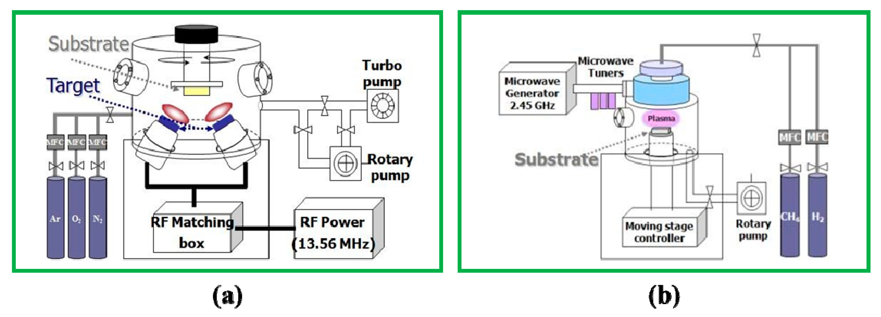
2. Experiment
2.1. Interlayer Deposition
2.2. Carbon Nanowall Growth
2.3. Analysis of the Samples
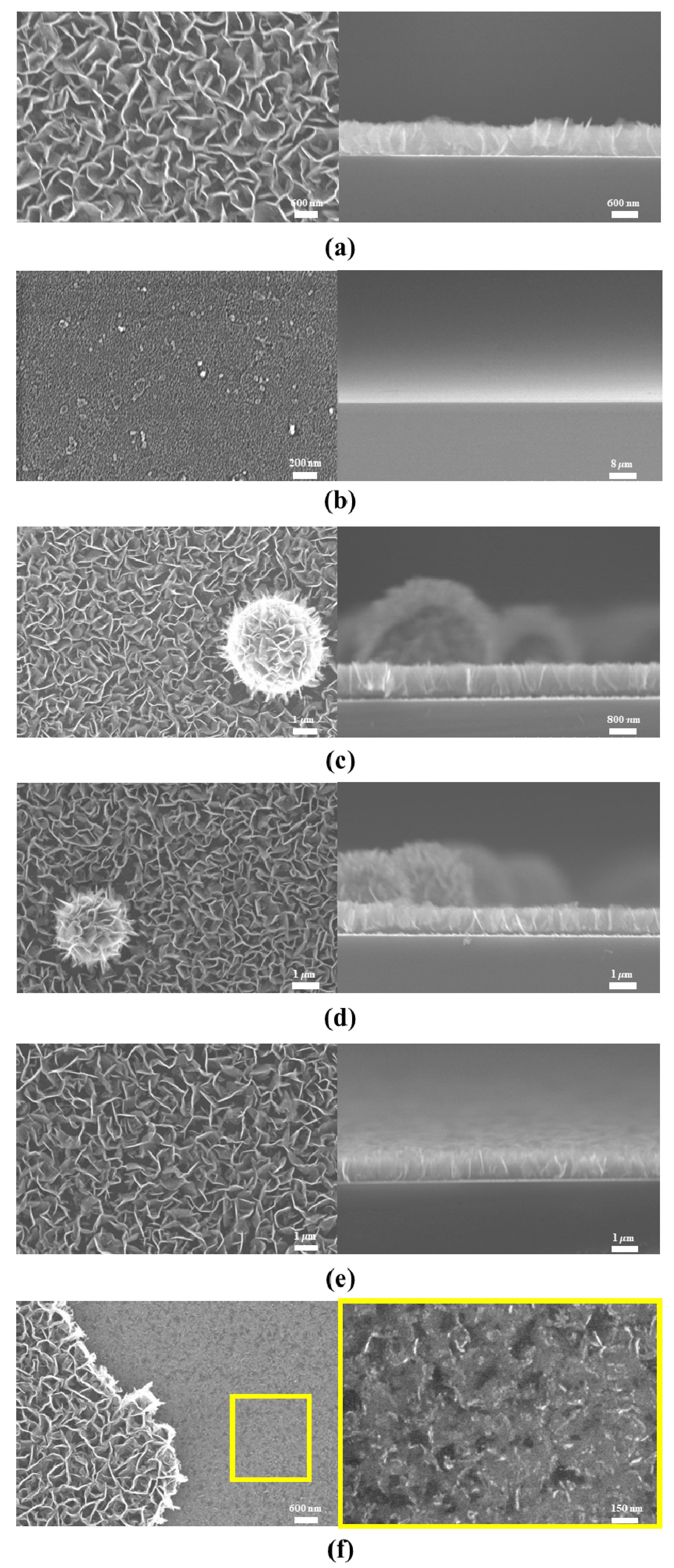
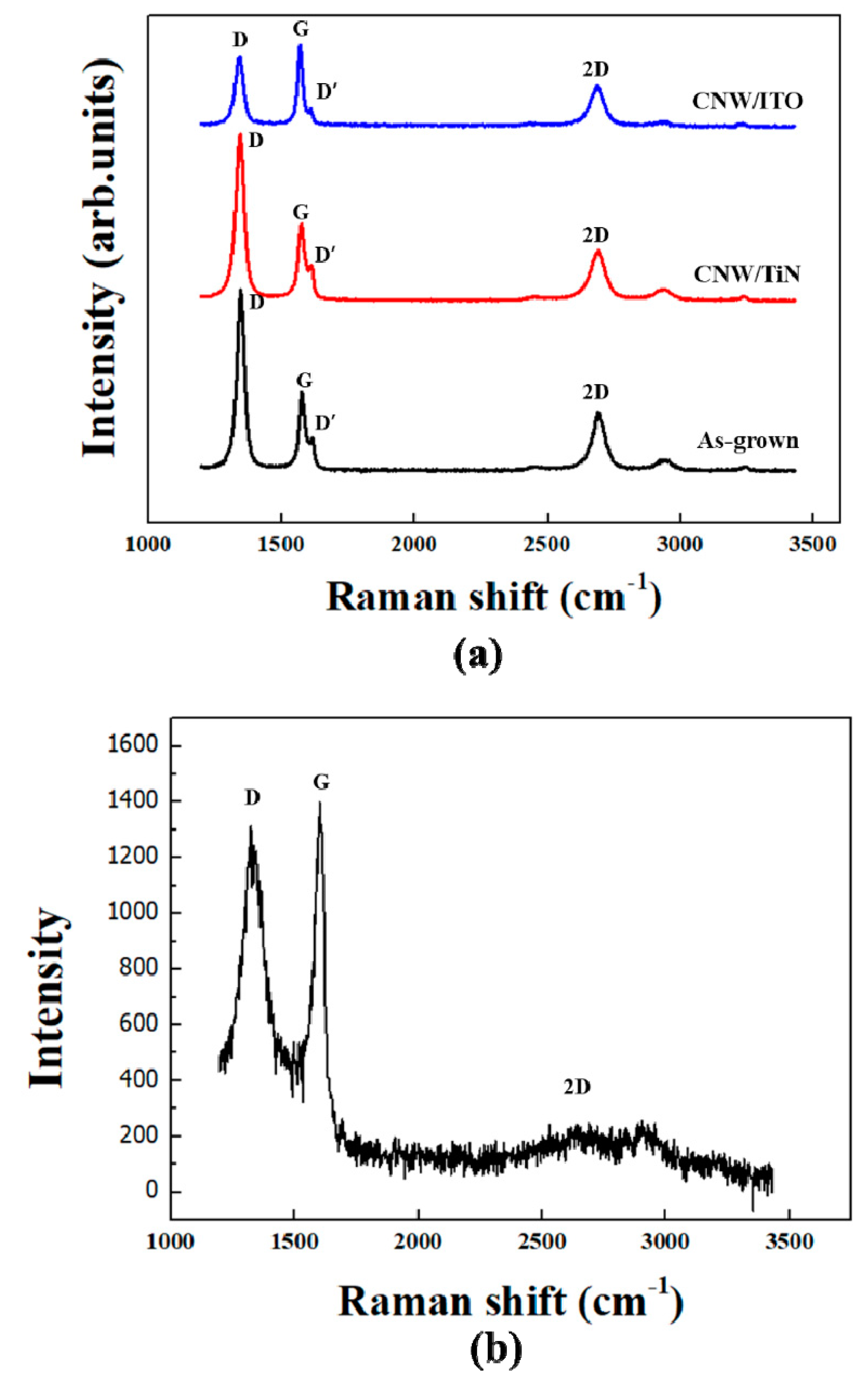
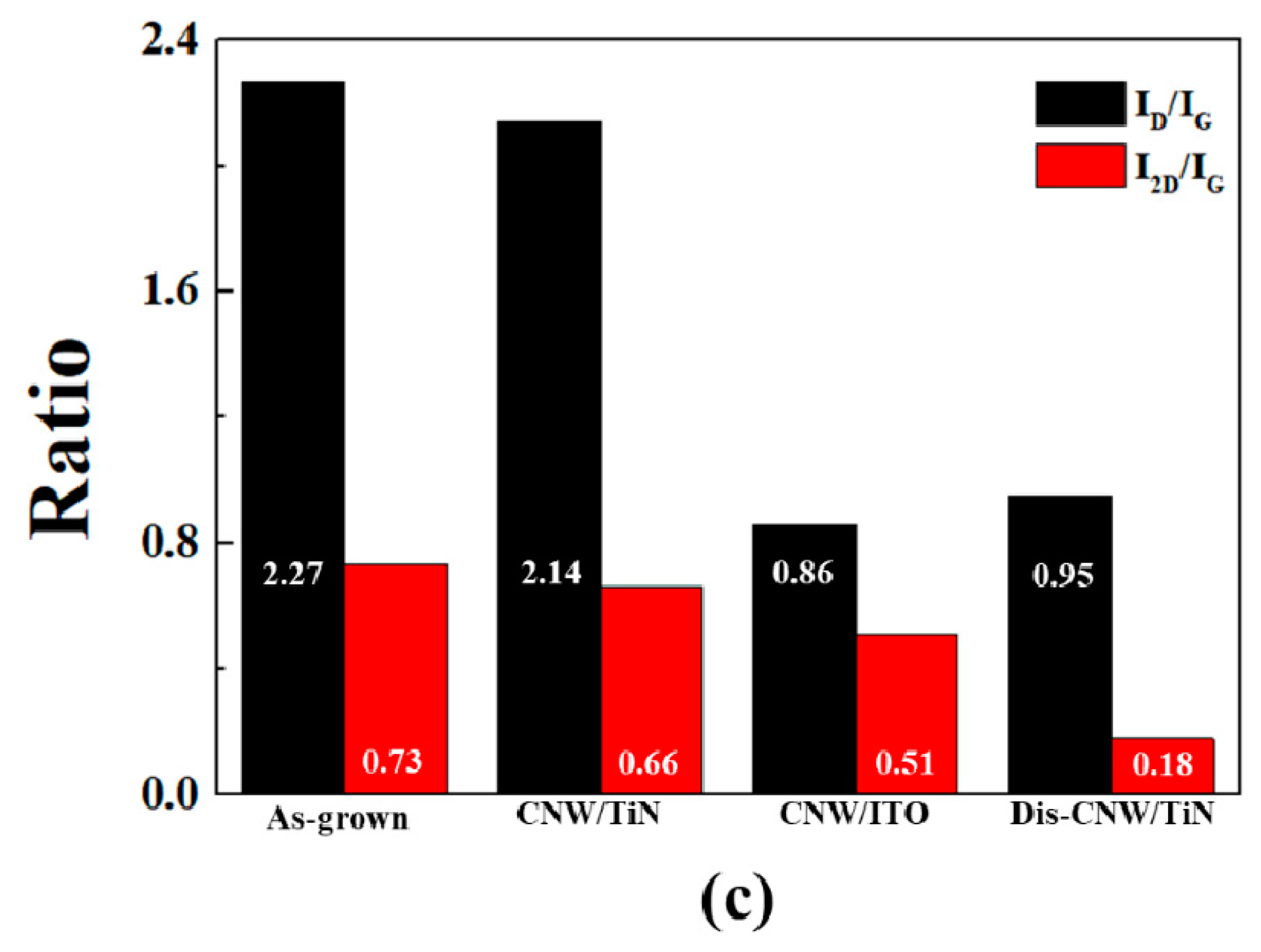
3. Results and Discussion
3.1. Structural Characteristics
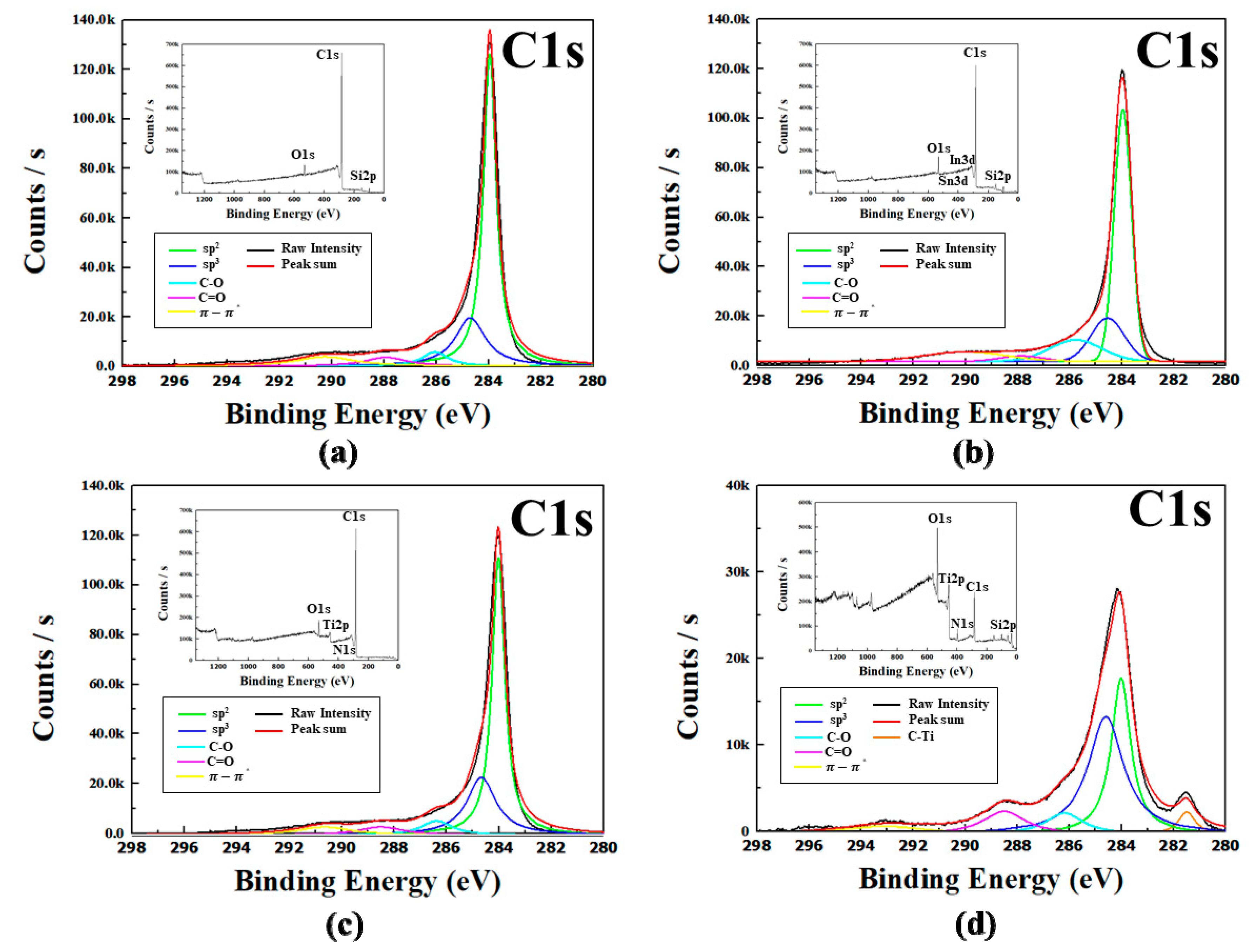
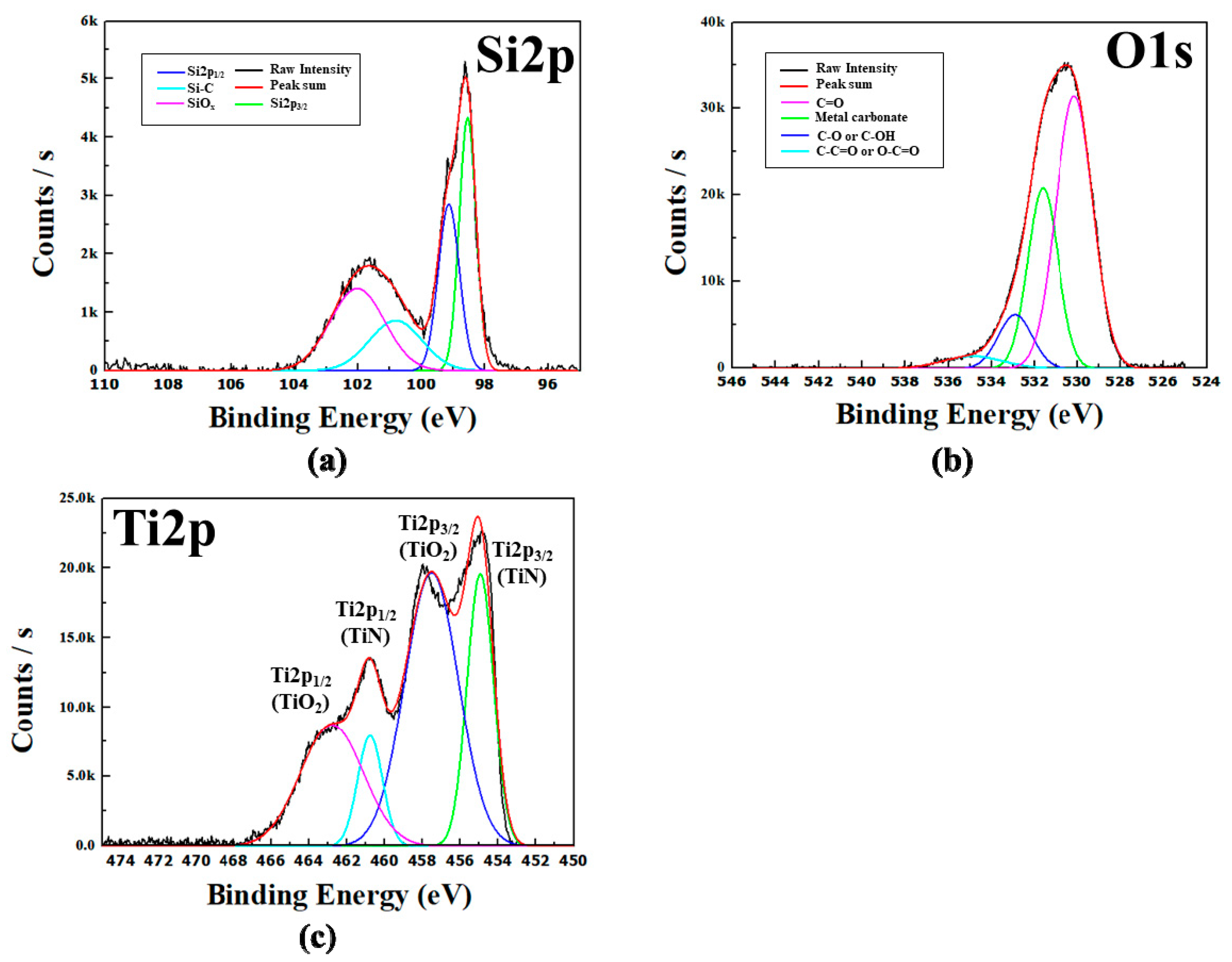
3.2. Chemical Properties
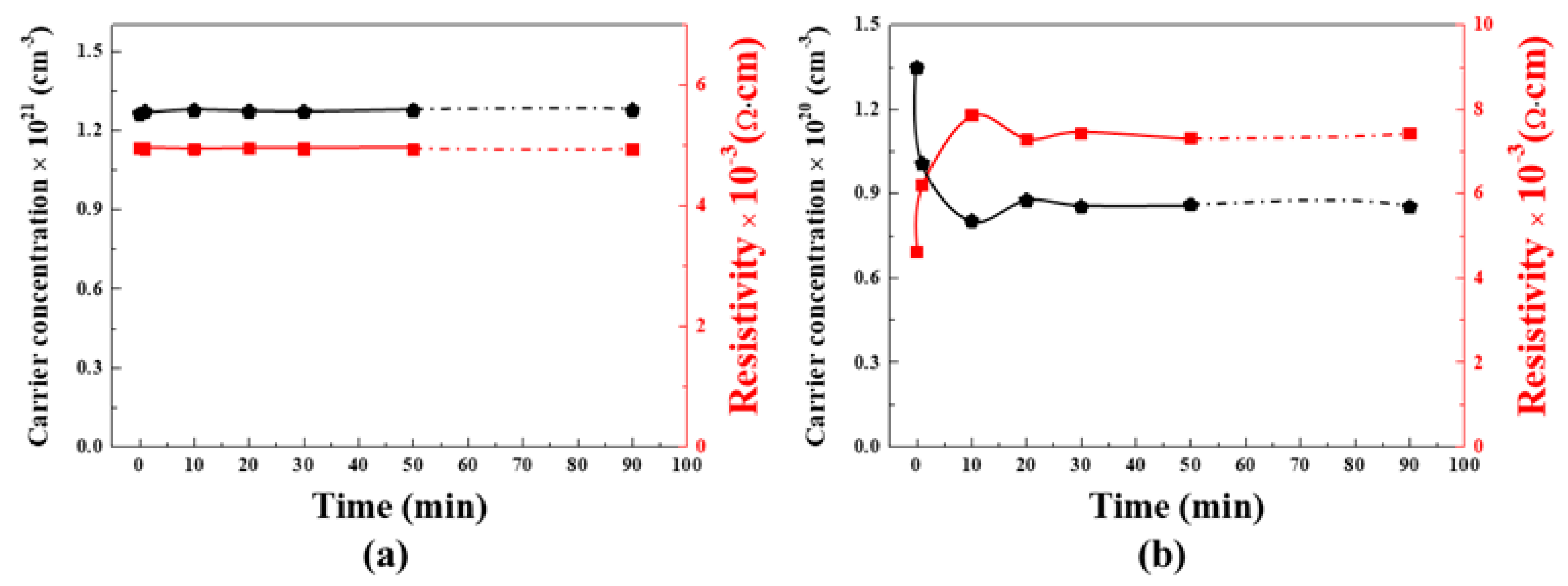
3.3. Electrical Characteristics
4. Conclusions
Author Contributions
Funding
Conflicts of Interest
References
- Sasikala, S.P.; Jeong, G.H.; Yun, T.; Kim, S.O. A perspective on R&D status of energy storage systems in South Korea. Energy Storage Mater 2019, 23, 154–158. [Google Scholar] [CrossRef]
- Liu, J.; Chen, X.; Yang, H.; Li, Y. Energy storage and management system design optimization for a photovoltaic integrated low-energy building. Energy 2019, 31, 116424. [Google Scholar] [CrossRef]
- Cheng, L.; Zhang, F.; Liu, S.; Zhang, Z. Configuration method of hybrid energy storage system for high power density in More Electric Aircraft. J. Power Sources 2020, 445, 227322, in press. [Google Scholar] [CrossRef]
- Zhang, K.; Hu, Z.; Chen, J. Functional porous carbon-based composite electrode materials for lithium secondary batteries. J. Energy Chem. 2013, 22, 214–225. [Google Scholar] [CrossRef]
- Yang, Q.; Li, J.W.S.; Zhang, L.; Fu, J.; Huang, F.; Cheng, Q. Vertically-oriented graphene nanowalls: Growth and application in Li-ion batteries. Diam. Relat. Mater. 2019, 91, 54–63. [Google Scholar] [CrossRef]
- Zhu, M.; Wang, J.; Holloway, B.C.; Outlaw, R.A.; Zhao, X.; Hou, K.; Shutthanan, V.; Manos, D.M. A mechanism for carbon nanosheet formation. Carbon 2007, 45, 2229–2234. [Google Scholar] [CrossRef]
- Zhao, J.; Shaygan, M.; Eckert, J.; Meyyappan, M.; Rümmeli, M.H. A Growth Mechanism for Free-Standing Vertical Graphene. Nano Lett. 2014, 14, 3064–3071. [Google Scholar] [CrossRef]
- Bo, Z.; Yang, Y.; Chen, J.; Yu, K.; Yan, J.; Cen, K. Plasam-enhanced chemical vapor deposition synthesis of vertically orented graphene nanosheets. Nanoscale 2013, 5, 5180. [Google Scholar] [CrossRef] [Green Version]
- Kumar, A.; Voevodin, A.A.; Zemlyanov, D.; Zakharov, D.N.; Fisher, T.S. Rapid synthesis of few-layer graphene over Cu foil. Carbon 2012, 50, 1546–1553. [Google Scholar] [CrossRef]
- Zhang, J.; Tahmasebi, A.; Omoriyekomwan, J.E.; Yu, J. Production of carbon nanotubes on bio-char at low temperature via microwave-assisted CVD using Ni catalyst. Diam. Relat. Mater. 2019, 91, 98–106. [Google Scholar] [CrossRef]
- Cui, L.; Chen, J.; Yang, B.; Sun, D.; Jiao, T. RF-PECVD synthesis of carbon nanowalls and their field emission properties. Appl. Surf. Sci. 2015, 357, 1–7. [Google Scholar] [CrossRef]
- Banerjee, D.; Mukherjee, S.; Chattopadhyay, K.K. Synthesis of amorphous carbon nanowalls by DC-PECVD on different substrates and study of its field emission properties. Appl. Surf. Sci. 2011, 257, 3717–3722. [Google Scholar] [CrossRef]
- Obraztsov, A.N.; Volkov, A.P.; Nagovitsyn, K.S.; Nishimura, K.; Morisawa, K.; Nakano, Y.; Hiraki, A. CVD growth and field emission properties of nanostructured carbon films. J. Phys. D Appl. Phys. 2002, 35, 357–362. [Google Scholar] [CrossRef]
- Kim, S.Y.; Shin, S.K.; Kim, H.; Jung, Y.H.; Kang, H.; Choi, W.S.; Kweon, G.B. Synthesis of Carbon Nanowalls by Microwave PECVD for Battery Electrode. Trans. Electr. Electron. Mater. 2015, 16, 198–200. [Google Scholar] [CrossRef] [Green Version]
- Obraztsov, A.N.; Pavlovsky, I.Y.; Volkov, A.P.; Petrov, A.S.; Petrov, V.I.; Rakova, E.V.; Roddatis, V.V. Electron field emission and structural properties of carbon chemically vapor-deposited films. Diam. Relat. Mater. 1999, 8, 814–819. [Google Scholar] [CrossRef]
- Lee, S.W.; Muoth, M.; Helbling, T.; Mattmann, M.; Hierold, C. Suppression of resist contamination during photolithography on carbon nanomaterials by a sacrificial layer. Carbon 2014, 66, 295–301. [Google Scholar] [CrossRef]
- Filippidou, M.K.; Chatzichristidi, M.; Chatzandroulis, S. A fabrication process of flexible IDE capacitive chemical sensors using a two step lift-off method based on PVA patterning. Sens. Actuators B Chem. 2019, 284, 7–12. [Google Scholar] [CrossRef]
- Aleksandrova, M.; Kurtev, N.; Videkov, V.; Tzanova, S.; Schintke, S. Material alternative to ITO for transparent conductive electrode in flexible display and photovoltaic devices. Microelectron. Eng. 2015, 145, 112–116. [Google Scholar] [CrossRef]
- Li, Z.H.; Cho, E.S.; Kwon, S.J. Laser direct patterning of the T-shaped ITO electrode for high-efficiency alternative current plasma display panels. Appl. Surf. Sci. 2010, 257, 776–780. [Google Scholar] [CrossRef]
- Virolainen, S.; Huhtanen, T.; Laitinen, A.; Sainio, T. Two alternative process routes for recovering pure indium from waste liquid crystal display panels. J. Clean. Prod. 2020, 243, 118599, in press. [Google Scholar] [CrossRef]
- Aal, A.A. Development of nickel coatings by TiN interlayer. Mater. Chem. Phys. 2007, 106, 317–322. [Google Scholar] [CrossRef]
- Zhou, B.; Liu, Z.; Piliptsou, D.G.; Rogachev, A.V.; Yu, S.; Wu, Y.; Tang, B.; Rudenkov, A.S. Growth feature of ionic nitrogen doped CNx bilayer films with Ti and TiN interlayer by pulse cathode arc discharge. Appl. Surf. Sci. 2016, 361, 169–176. [Google Scholar] [CrossRef]
- Kern, W.; Puotinen, D.A. Cleaning solutions based on hydrogen peroxide for use in silicon semiconductor technology. RCA Rev. 1970, 31, 187. [Google Scholar]
- Malard, L.M.; Pimenta, M.A.; Dresselhaus, G.; Dresselhaus, M.S. Raman spectroscopy in graphene. Phys. Rep. 2009, 473, 51–87. [Google Scholar] [CrossRef]
- Pérez, L.A.; Bajales, N.; Lacconi, G.I. Raman spectroscopy coupled with AFM scan head: A versatile combination for tailoring graphene oxide/reduced graphene oxide hybrid materials. Appl. Surf. Sci. 2019, 495, 143539. [Google Scholar] [CrossRef]
- Graf, D.; Molitor, F.; Ensslin, K.; Stampfer, C.; Jungen, A.; Hierold, C.; Witz, L. Spatially resolved Raman spectroscopy of single-and few-layer graphene. Nano Lett. 2007, 7, 238–242. [Google Scholar] [CrossRef] [Green Version]
- Ferrari, A.C.; Meyer, J.C.; Scardaci, V.; Casiraghi, C.; Lazzeri, M.; Mauri, F.; Piscanec, S.; Jiang, D.; Novoselov, K.S.; Roth, S.; et al. Raman spectrum of graphene and graphene layers. Phys. Rev. Lett. 2006, 97, 187401–187404. [Google Scholar] [CrossRef] [Green Version]
- Soin, N.; Roy, S.S.; Ray, S.C.; McLaughlin, J.A. Excitation energy dependence of Raman bands in multiwalled carbon nanotubes. J. Raman Spectrosc. 2010, 41, 1227–1233. [Google Scholar] [CrossRef]
- Al-Gaashani, R.; Najjar, A.; Zakaria, Y.; Mansour, S.; Atieha, M.A. XPS and structural studies of high quality graphene oxide and reduced graphene oxide prepared by different chemical oxidation methods. Ceram. Int. 2019, 45, 14439–14448. [Google Scholar] [CrossRef]
- Ederer, J.; Janoš, P.; Ecorchard, P.; Tolasz, J.; Štengl, V.; Beneš, H.; Perchacz, M.; Pop-Georgievski, O. Determination of amino groups on functionalized graphene oxide for polyurethane nanomaterials: XPS quantitation vs. functional speciation. RSC Adv. 2017, 21, 12464–12473. [Google Scholar] [CrossRef] [Green Version]
- Zhang, L.X.; Sun, Z.; Qi, J.L.; Shi, J.M.; Hao, T.D.; Feng, J.C. Understanding the growth mechanism of vertically aligned graphene and control of its wettability. Carbon 2016, 103, 339–345. [Google Scholar] [CrossRef]
- Vitos, L.; Ruban, A.V.; Skriver, H.L.; Kollár, J. The surface energy of metals. Surf. Sci. 1998, 411, 186–202. [Google Scholar] [CrossRef]
- Lim, W.; Ahn, Y.; Lee, S.; An, I.; Lee, C. The stability of ITO, AZO and SZO thin films in hydrogen plasma. J. Korean Vac. Soc. 1997, 6, 227–234. [Google Scholar]
- Lee, J.; Lim, D.; Yang, K.; Choi, W. Influence of different plasma treatments on electrical and optical properties on sputtered AZO and ITO films. J. Cryst. Growth. 2011, 326, 50–57. [Google Scholar] [CrossRef]
- Yue, Z.; Zhou, L.; Jin, C.; Liu, L.; Xu, G.; Tang, H.; Huang, H.; Yuan, J.; Gao, C. Study on the effect of intrinsic electrical resistivity of silicon materials on its performance for Li-ion batteries. Mater. Lett. 2017, 186, 217–219. [Google Scholar] [CrossRef]
- Akherat, S.J.M.; Karimi, M.A.; Alizadehyazdi, V.; Asalzadeh, S.; Spenko, M. A tunable dielectric to improve electrostatic adhesion in electrostatic/microstructured adhesives. J. Electrostat. 2019, 97, 58–70. [Google Scholar] [CrossRef]


| Samples | C | N | O | Si | In | Sn | Ti |
|---|---|---|---|---|---|---|---|
| Catalyst island of CNW/ITO | 56.71 | - | 8.24 | 9.23 | 17.81 | 8.02 | - |
| Other parts of CNW/ITO | 53.69 | - | 0.74 | 45.38 | 0.03 | 0.16 | - |
| CNW/TiN | 74.44 | 2.94 | - | 22.03 | - | - | 0.57 |
| Dissociated CNW/TiN | 16.69 | 1.50 | 8.00 | 72.37 | - | - | 1.44 |
© 2019 by the authors. Licensee MDPI, Basel, Switzerland. This article is an open access article distributed under the terms and conditions of the Creative Commons Attribution (CC BY) license (http://creativecommons.org/licenses/by/4.0/).
Share and Cite
Choi, H.; Kwon, S.; Kang, H.; Kim, J.H.; Choi, W. Adhesion-Increased Carbon Nanowalls for the Electrodes of Energy Storage Systems. Energies 2019, 12, 4759. https://doi.org/10.3390/en12244759
Choi H, Kwon S, Kang H, Kim JH, Choi W. Adhesion-Increased Carbon Nanowalls for the Electrodes of Energy Storage Systems. Energies. 2019; 12(24):4759. https://doi.org/10.3390/en12244759
Chicago/Turabian StyleChoi, Hyeokjoo, Seokhun Kwon, Hyunil Kang, Jung Hyun Kim, and Wonseok Choi. 2019. "Adhesion-Increased Carbon Nanowalls for the Electrodes of Energy Storage Systems" Energies 12, no. 24: 4759. https://doi.org/10.3390/en12244759