Voltage Balance Switching Scheme for Series-Connected SiC MOSFET LLC Resonant Converter


Abstract
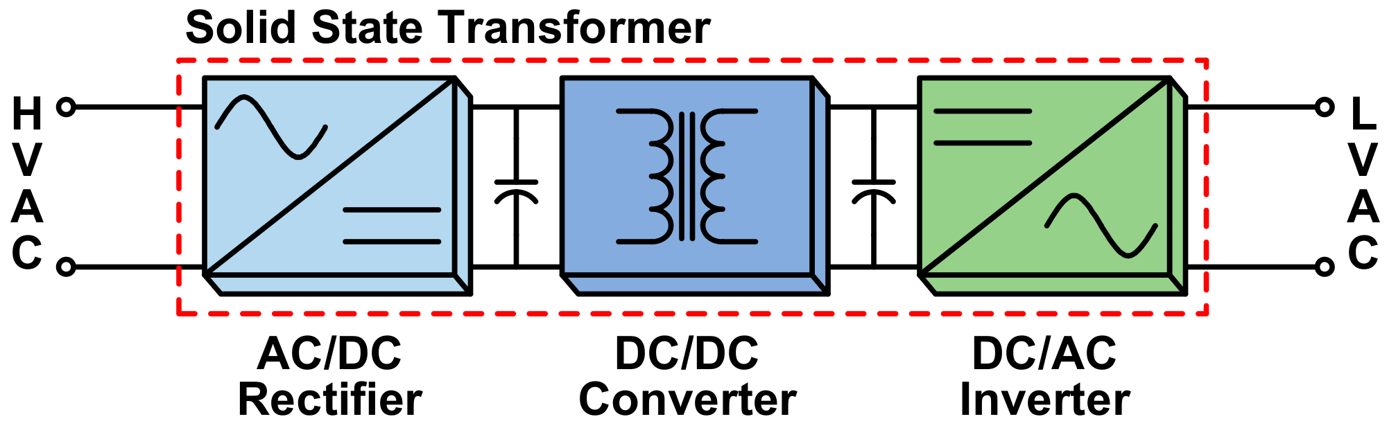
:1. Introduction
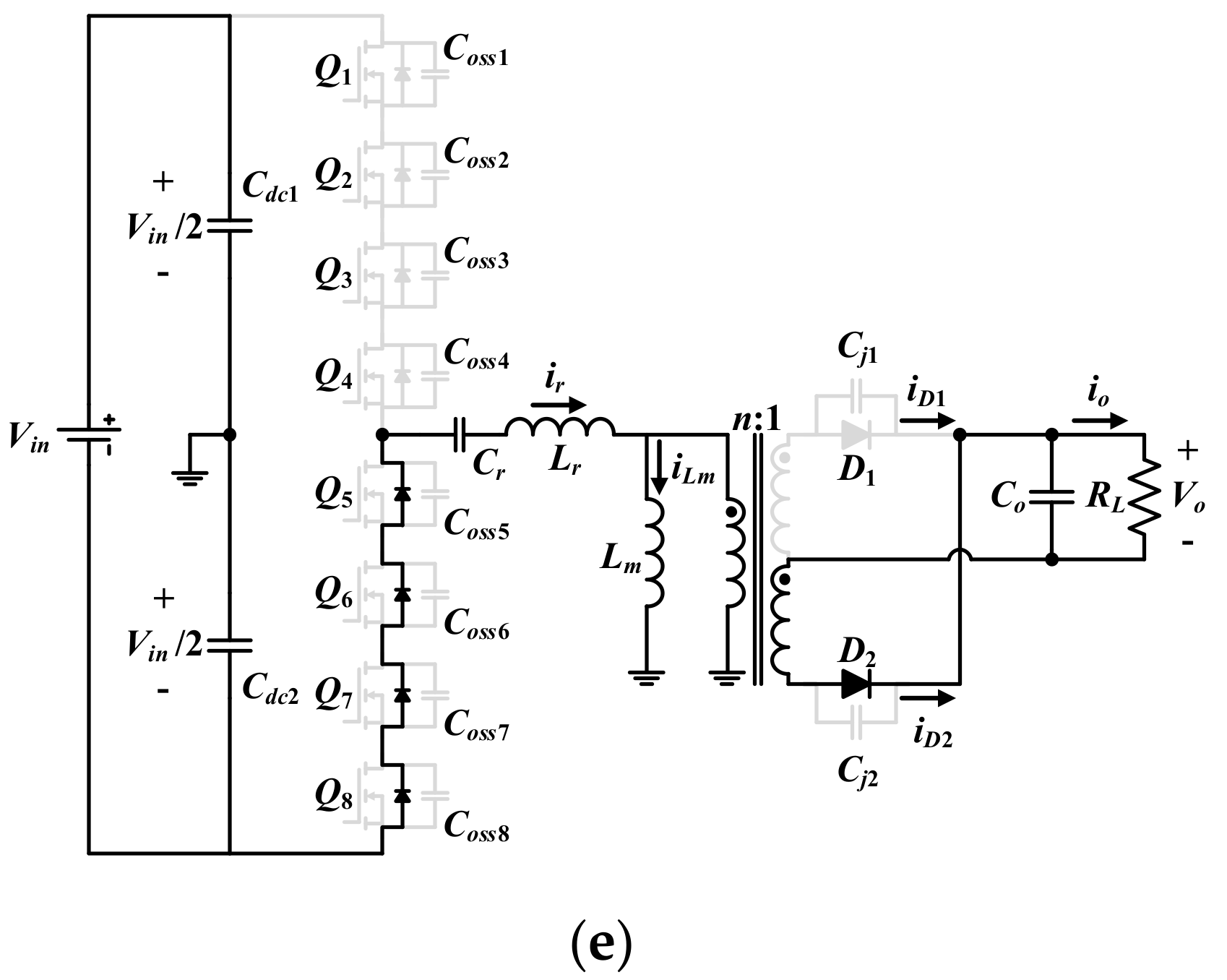
2. Series-Connected SiC-MOSFET LLC Resonant Converter
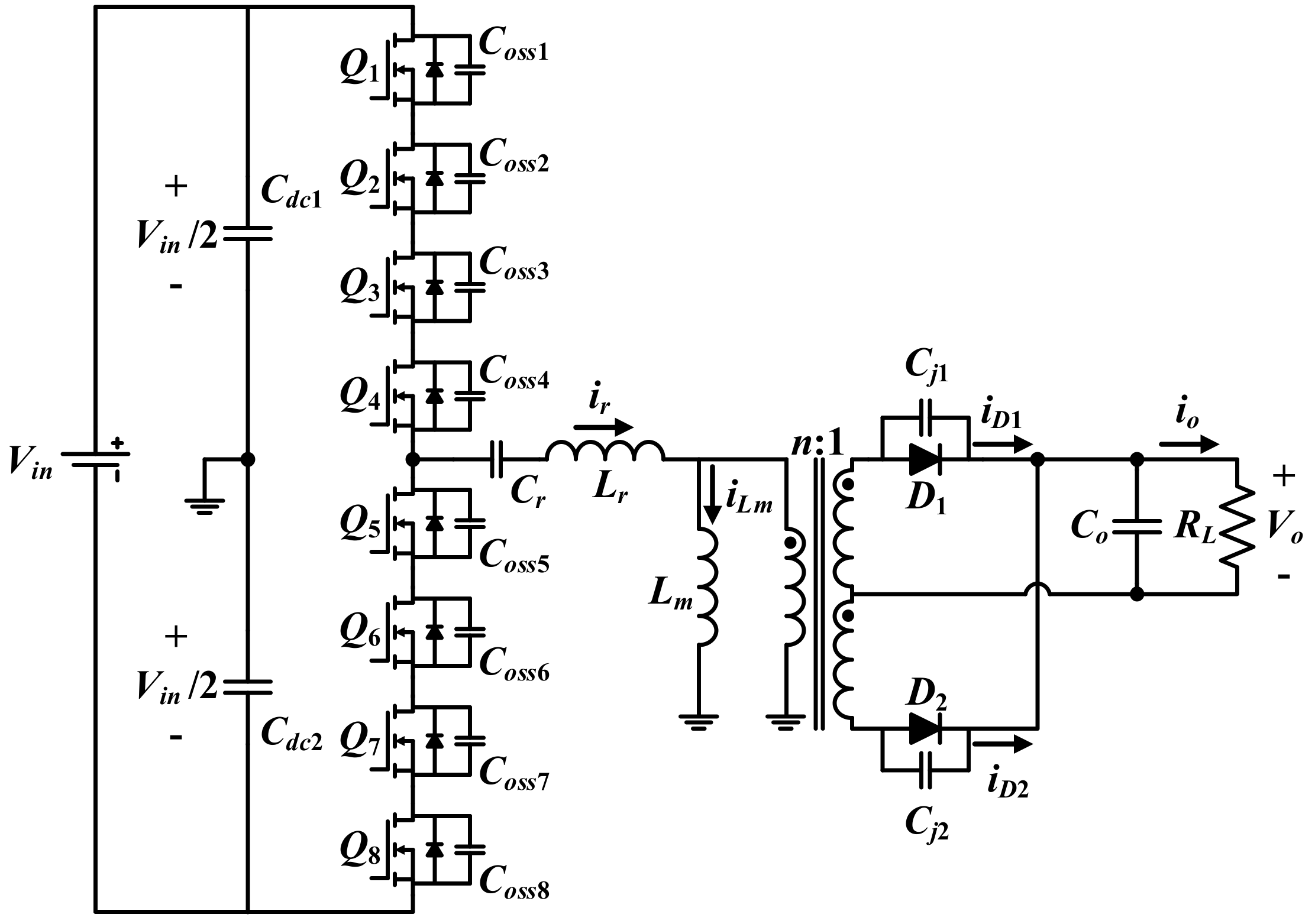
2.1. System Description
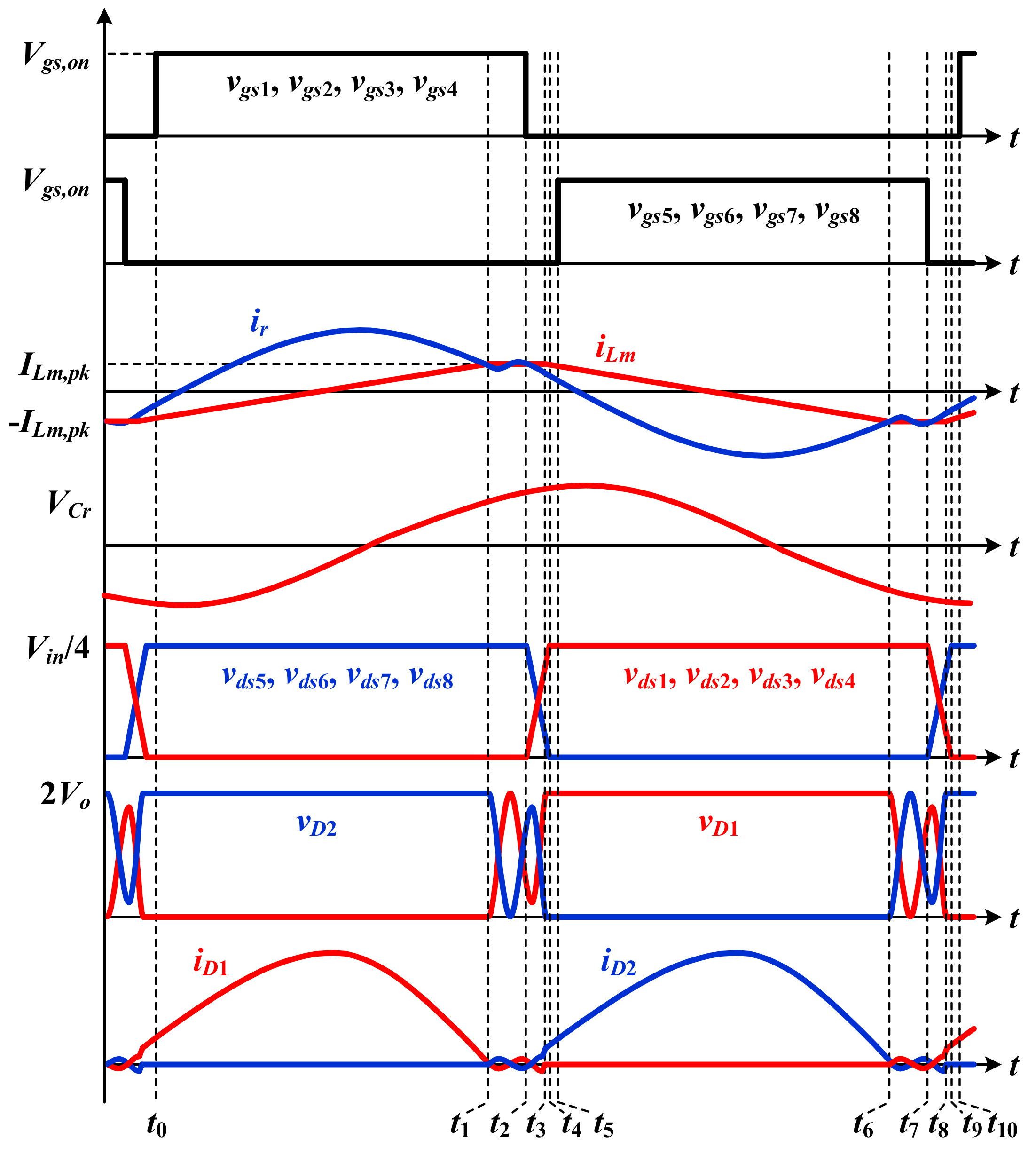
2.2. Operating Principle
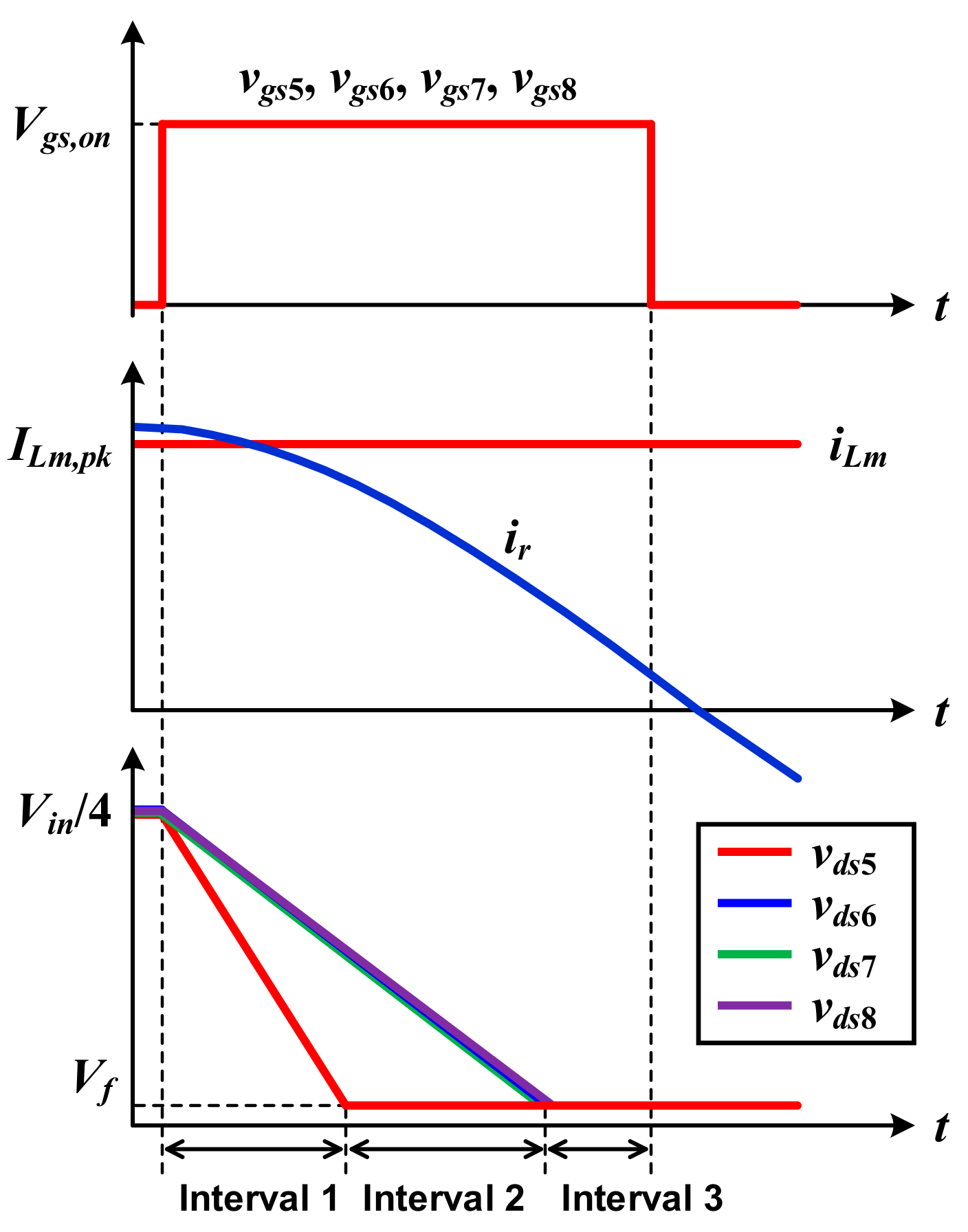
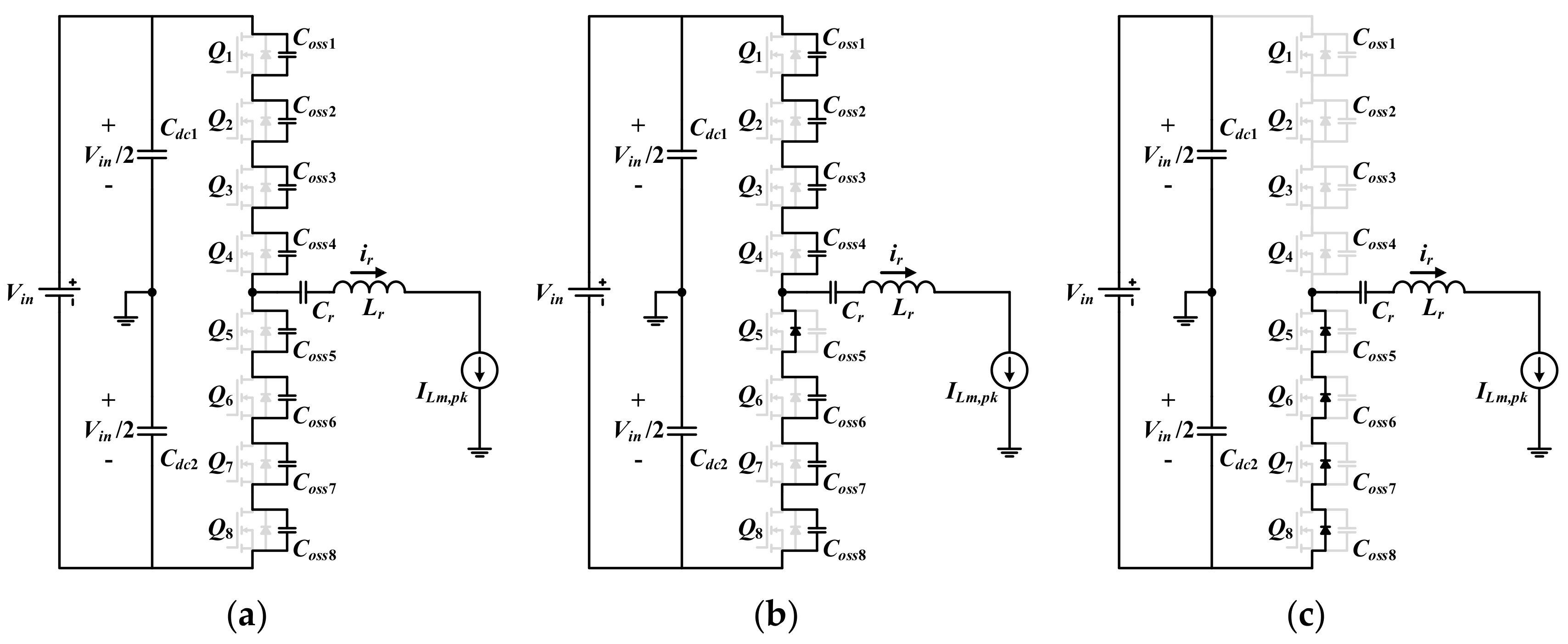
3. Analysis of Voltage Imbalance in the Series-Connected SiC MOSFET LLC Resonant Converter
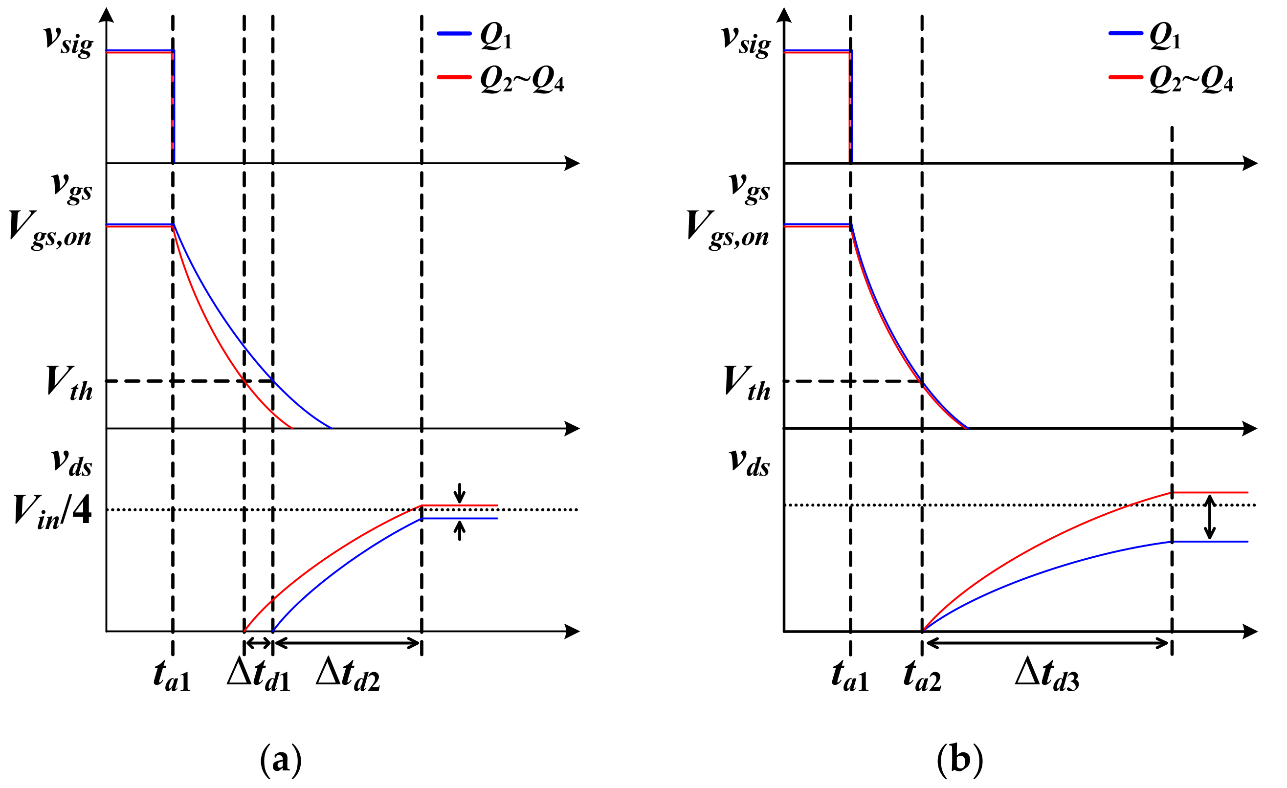
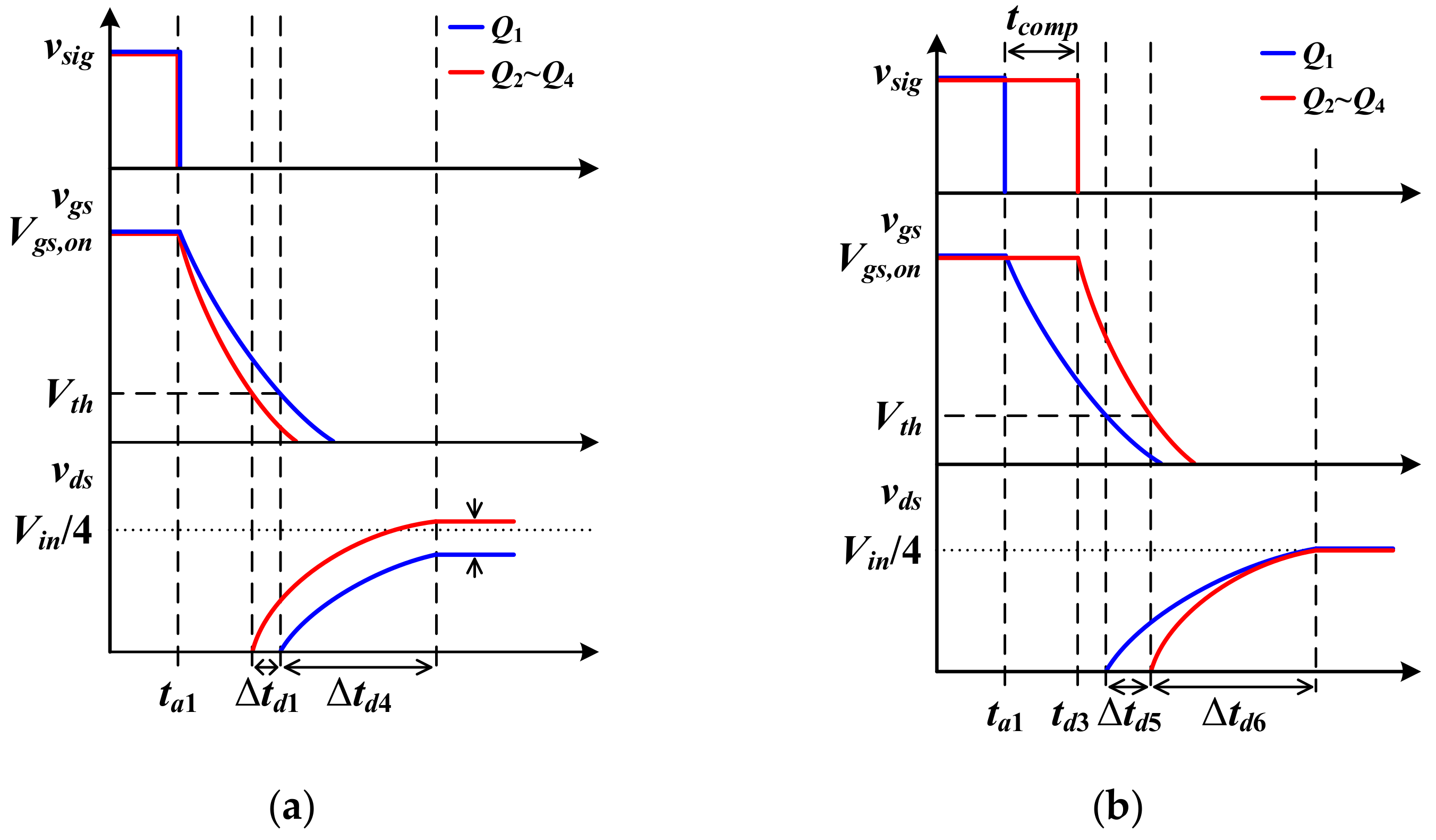
3.1. Turn-On Switching Characteristics
3.2. Turn-Off Switching Characteristics
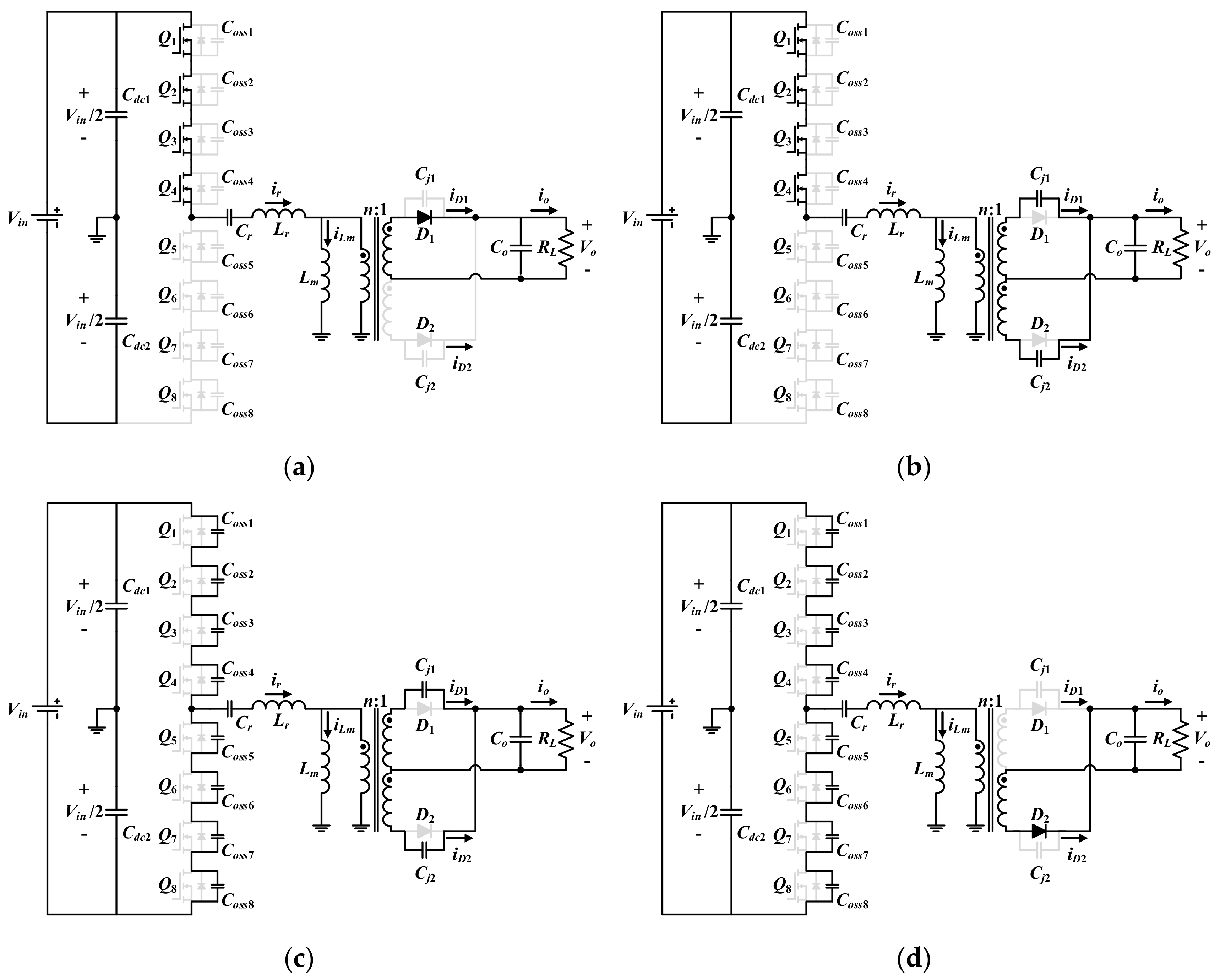
4. Proposed Switching Scheme
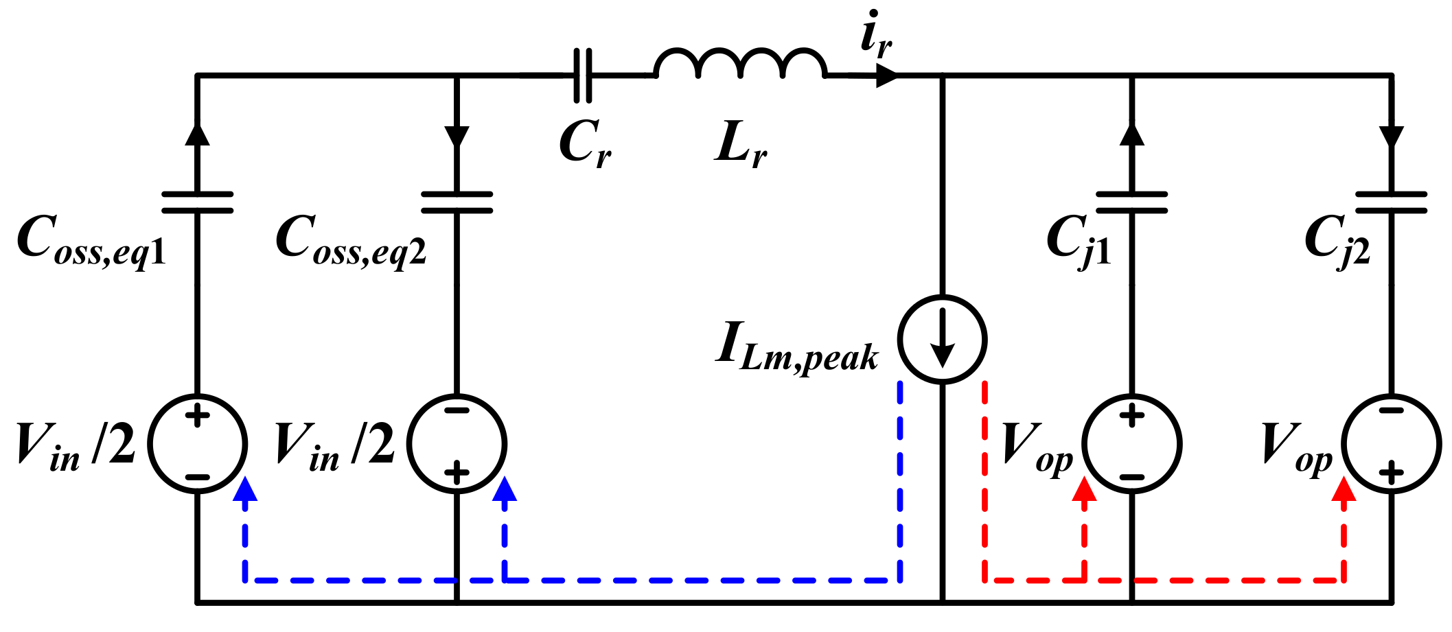
5. Design Considerations for Achieving ZVS
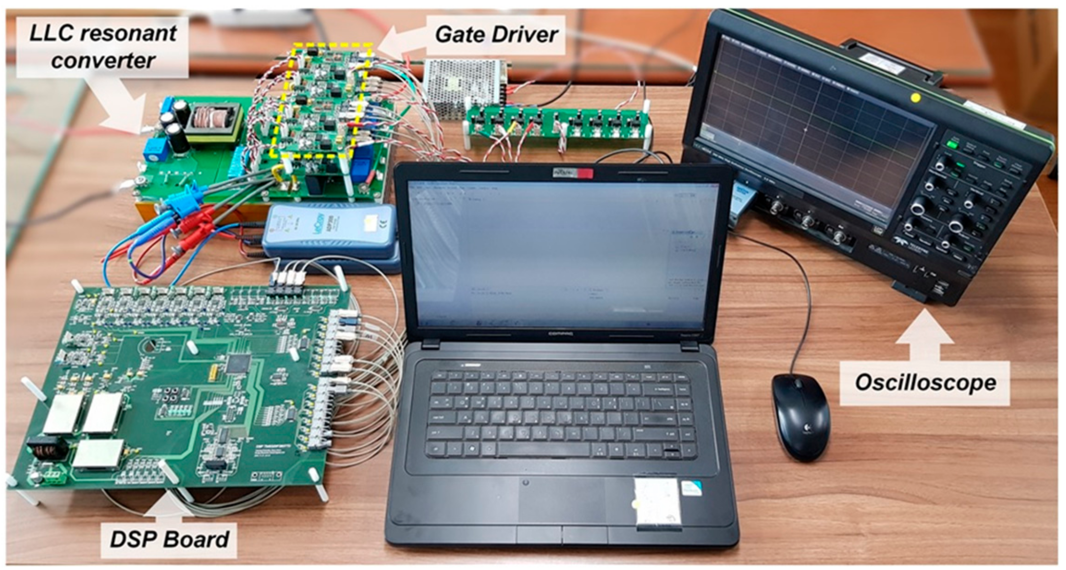
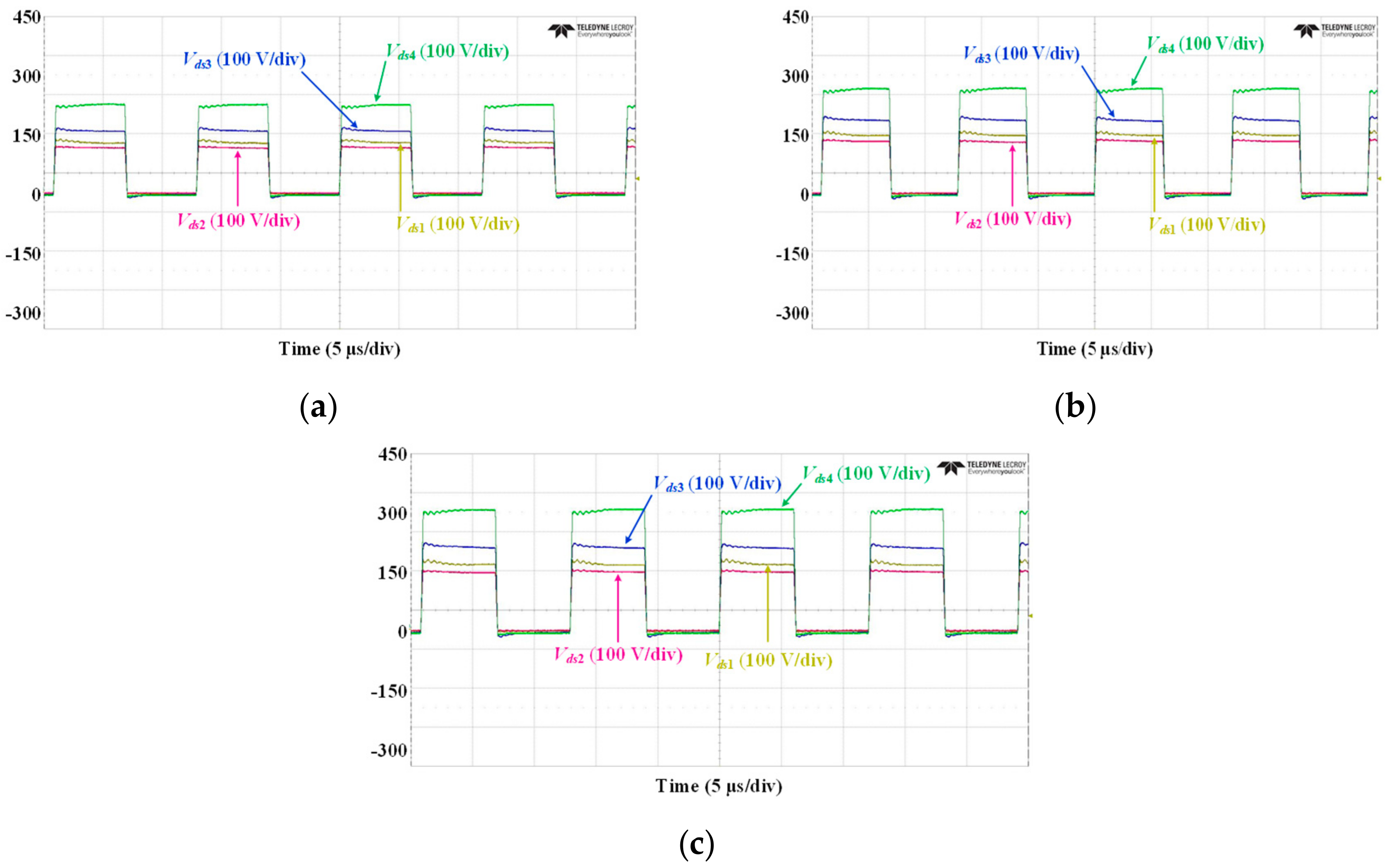
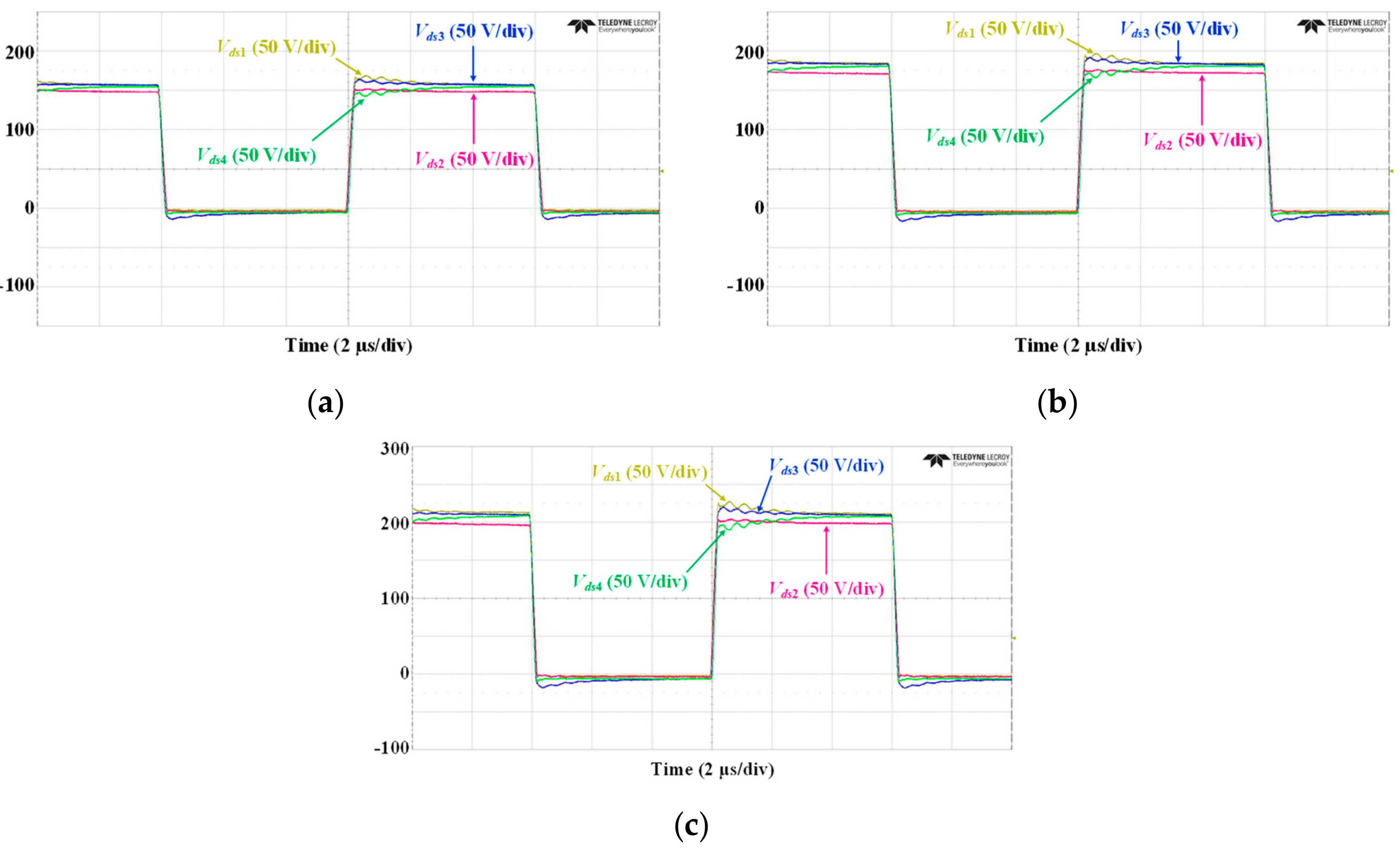
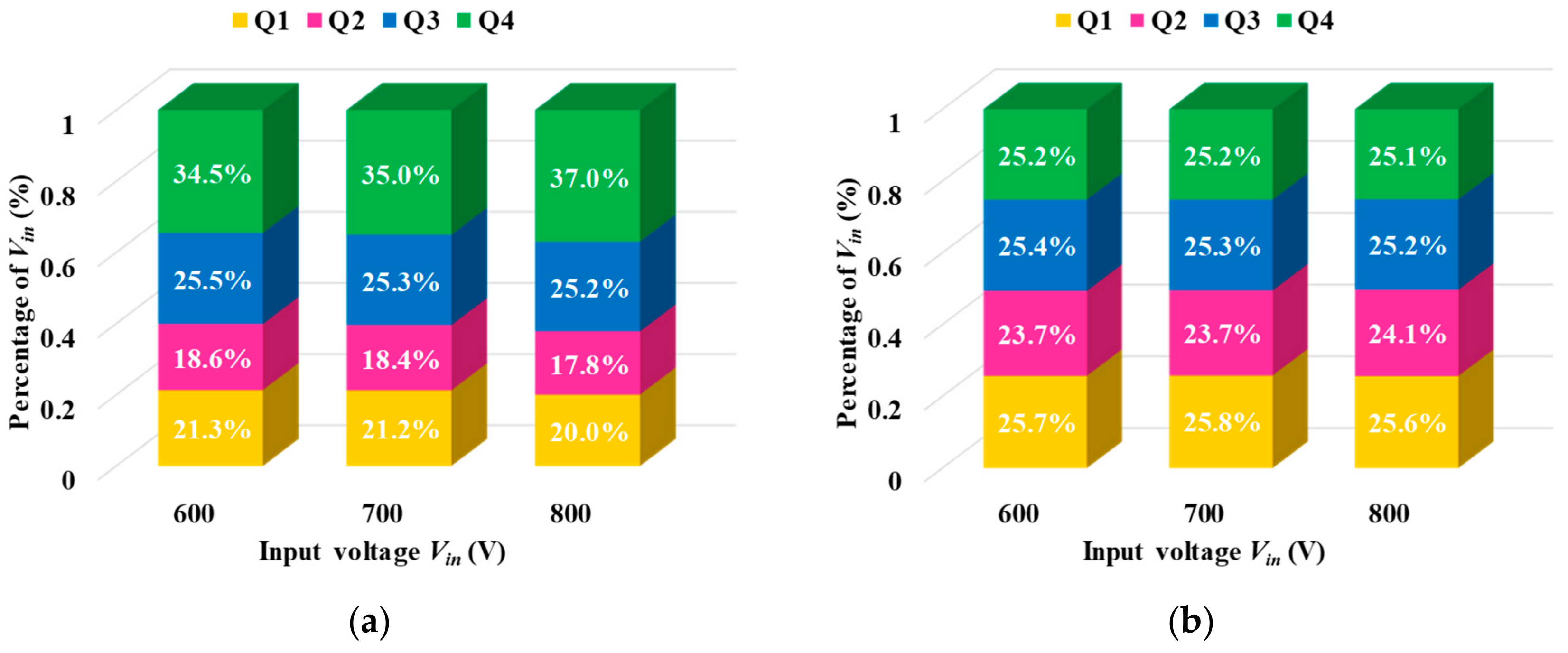
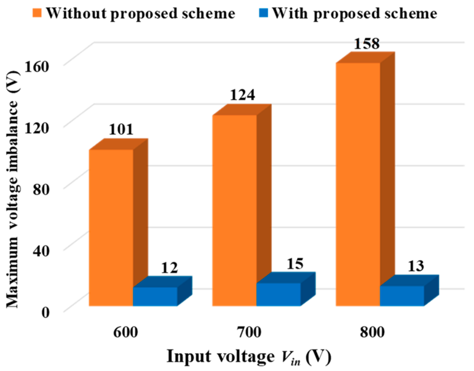
6. Experimental Results
7. Conclusions
Author Contributions
Funding
Conflicts of Interest
References
- She, X.; Yu, X.; Wang, F.; Huang, A.Q. Design and demonstration of a 3.6-kV–120-V/10-kVA solid-state transformer for smart grid application. IEEE Trans. Power Electron. 2014, 29, 3982–3996. [Google Scholar] [CrossRef]
- Zhao, T.; Wang, G.; Bhattacharya, S.; Huang, A.Q. Voltage and power balance control for a cascaded H-bridge converter-based solid-state transformer. IEEE Trans. Power Electron. 2013, 28, 1523–1532. [Google Scholar] [CrossRef]
- Tan, K.; Yu, R.; Guo, S.; Huang, A.Q. Optimal design methodology of bidirectional LLC resonant DC/DC converter for solid state transformer application. In Proceedings of the IECON 2014-40th Annual Conference of the IEEE Industrial Electronics Society, Dallas, TX, USA, 29 October–1 November 2014; pp. 1657–1664. [Google Scholar]
- Falcones, S.; Ayyanar, R.; Mao, X. A DC–DC multiport-converter-based solid-state transformer integrating distributed generation and storage. IEEE Trans. Power Electron. 2013, 28, 2192–2203. [Google Scholar] [CrossRef]
- Basu, K.; Shahani, A.; Sahoo, A.K.; Mohan, N. A single-stage solid-state transformer for PWM AC drive with source-based commutation of leakage energy. IEEE Trans. Power Electron. 2015, 30, 1734–1746. [Google Scholar] [CrossRef]
- Fan, H.; Li, H. High-frequency transformer isolated bidirectional DC-DC converter modules with high efficiency over wide load range for 20 kVA solid-state transformer. IEEE Trans. Power Electron. 2011, 26, 3599–3608. [Google Scholar] [CrossRef]
- Falcones, S.; Mao, X.; Ayyanar, R. Topology comparison for solid state transformer implementation. In Proceedings of the IEEE PES General Meeting, Providence, RI, USA, 25–29 July 2010; pp. 1–8. [Google Scholar]
- Qin, H.; Kimball, J.W. Closed-loop control of DC-DC dual-active-bridge converters driving single-phase inverters. IEEE Trans. Power Electron. 2014, 29, 1006–1017. [Google Scholar]
- Itoh, J.-I.; Aoyagi, K.; Nakanishi, T. Bidirectional single-phase Solid-State Transformer using multi cell for volume reduction of high voltage capacitor. In Proceedings of the 2017 IEEE 3rd International Future Energy Electronics Conference and ECCE Asia (IFEEC 2017-ECCE Asia), Kaohsiung, Taiwan, 3–7 June 2017; pp. 332–337. [Google Scholar]
- Dujic, D.; Steinke, G.K.; Bellini, M.; Rahimo, M.; Storasta, L.; Steinke, J.K. Characterization of 6.5 kV IGBTs for high-power medium-frequency soft-switched applications. IEEE Trans. Power Electron. 2014, 29, 906–919. [Google Scholar] [CrossRef]
- Lai, J.-S.; Choe, J.M.; Yeh, C.-S.; Moon, S.-R.; Lai, W.-H.; Zhang, L. A modular front-end medium-voltage solid-state transformer. In Proceedings of the 2017 Asian Conference on Energy, Power and Transportation Electrification (ACEPT), Singapore, 24–26 October 2017; pp. 1–6. [Google Scholar]
- Lee, M.; Kim, J.-W.; Lai, J.-S. Small-signal modeling of three-level boost rectifier and system design for medium-voltage solid-state transformer. In Proceedings of the 2019 10th International Conference on Power Electronics and ECCE Asia (ICPE 2019-ECCE Asia), Busan, Korea, 27–30 May 2019; pp. 1–7. [Google Scholar]
- Hazra, S.; De, A.; Cheng, L.; Palmour, J.; Schupbach, M.; Hull, B.A.; Allen, S.; Bhattacharya, S. High switching performance of 1700-V, 50-A SiC power MOSFET over Si IGBT/BiMOSFET for advanced power conversion applications. IEEE Trans. Power Electron. 2016, 31, 4742–4754. [Google Scholar]
- Millán, J.; Godignon, P.; Perpiñà, X.; Pérez-Tomás, A.; Rebollo, J. A survey of wide bandgap power semiconductor devices. IEEE Trans. Power Electron. 2014, 29, 2155–2163. [Google Scholar] [CrossRef]
- Mitova, R.; Ghosh, R.; Mhaskar, U.; Klikic, D.; Wang, M.-X.; Dentella, A. Investigations of 600-V GaN HEMT and GaN diode for power converter applications. IEEE Trans. Power Electron. 2014, 29, 2441–2452. [Google Scholar] [CrossRef]
- Nawaz, M.; Ilves, K. On the comparative assessment of 1.7 kV, 300 A full SiC-MOSFET and Si-IGBT power modules. In Proceedings of the 2016 IEEE Applied Power Electronics Conference and Exposition (APEC), Long Beach, CA, USA, 20–24 March 2016; pp. 276–282. [Google Scholar]
- Wang, X.; Jiang, C.; Lei, B.; Teng, H.; Bai, H.K.; Kirtley, J.L. Power-loss analysis and efficiency maximization of a silicon-carbide MOSFET-based three-phase 10-kW bidirectional EV charger using variable-DC-bus control. IEEE J. Emerg. Sel. Top. Power Electron. 2016, 4, 880–892. [Google Scholar] [CrossRef]
- Nakakohara, Y.; Otake, H.; Evans, T.M.; Yoshida, T.; Tsuruya, M.; Nakahara, K. Three-phase LLC series resonant DC/DC converter using SiC MOSFETs to realize high-voltage and high-frequency operation. IEEE Trans. Ind. Electron. 2016, 63, 2103–2110. [Google Scholar] [CrossRef]
- Zhang, W.; Long, Y.; Zhang, Z.; Wang, F.; Tolbert, L.M.; Blalock, B.J.; Henning, S.; Wilson, C.; Dean, R. Evaluation and comparison of silicon and gallium nitride power transistors in LLC resonant converter. In Proceedings of the 2012 IEEE Energy Conversion Congress and Exposition (ECCE), Raleigh, NC, USA, 15–20 September 2012; pp. 1362–1366. [Google Scholar]
- Zhang, W.; Xu, Z.; Zhang, Z.; Wang, F.; Tolbert, L.M.; Blalock, B.J. Evaluation of 600 V cascode GaN HEMT in device characterization and all-GaN-based LLC resonant converter. In Proceedings of the 2013 IEEE Energy Conversion Congress and Exposition (ECCE), Denver, CO, USA, 15–19 September 2013; pp. 3571–3578. [Google Scholar]
- Zhang, W.; Wang, F.; Costinett, D.J.; Tolbert, L.M.; Blalock, B.J. Investigation of gallium nitride devices in high-frequency LLC resonant converters. IEEE Trans. Power Electron. 2017, 32, 571–583. [Google Scholar] [CrossRef]
- Vechalapu, K.; Bhattacharya, S.; Aleoiza, E. Performance evaluation of series connected 1700V SiC MOSFET devices. In Proceedings of the 3rd IEEE Workshop on Wide Bandgap Power Devices and Applications (WiPDA), Blacksburg, VA, USA, 2–4 November 2015; pp. 184–191. [Google Scholar]
- Vechalapu, K.; Kadavelugu, A.K.; Bhattacharya, S. High voltage dual active bridge with series connected high voltage silicon carbide (SiC) devices. In Proceedings of the 2014 IEEE Energy Conversion Congress and Exposition (ECCE), Pittsburgh, PA, USA, 14–18 September 2014; pp. 2057–2064. [Google Scholar]
- Han, Y.; Chen, W.; Chen, X.; Ma, X.; Sha, Y.; Yang, X.; Li, X. A 4000V input auxiliary power supply with series connected SiC MOSFETs for MMC-based HVDC system. In Proceedings of the 2016 IEEE 8th International Power Electronics and Motion Control Conference (IPEMC-ECCE Asia), Hefei, China, 22–26 May 2016; pp. 279–284. [Google Scholar]
- Vechalapu, K.; Bhattacharya, S. Performance comparison of 10 kV–15 kV high voltage SiC modules and high voltage switch using series connected 1.7 kV LV SiC MOSFET devices. In Proceedings of the 2016 IEEE Energy Conversion Congress and Exposition (ECCE), Milwaukee, WI, USA, 18–22 September 2016; pp. 1–8. [Google Scholar]
- Gonzalez, J.O.; Alatise, O.; Hu, J.; Ran, L.; Mawby, P.A. An investigation of temperature-sensitive electrical parameters for SiC power MOSFETs. IEEE Trans. Power Electron. 2017, 32, 7954–7966. [Google Scholar] [CrossRef]
- Chen, X.; Yu, L.; Jiang, T.; Tian, H.; Huang, K.; Wang, J. A high-voltage solid-state switch based on series connection of IGBTs for PEF applications. IEEE Trans. Plamsa Sci. 2017, 45, 2328–2334. [Google Scholar] [CrossRef]
- Palmer, P.R.; Zhang, J.; Zhang, X. SiC MOSFETs connected in series with active voltage control. In Proceedings of the 3rd IEEE Workshop on Wide Bandgap Power Devices and Applications (WiPDA), Blacksburg, VA, USA, 2–4 November 2015; pp. 60–65. [Google Scholar]
- Palmer, P.; He, W.; Zhang, X.; Zhang, J.; Snook, M. IGBT series connection under Active Voltage Control with temporary clamp. In Proceedings of the IECON 2012-38th Annual Conference on IEEE Industrial Electronics Society, Montreal, QC, Canada, 25–28 October 2012; pp. 465–470. [Google Scholar]
- Yang, X.; Zhang, J.; He, W.; Long, Z.; Palmer, P.R. Physical investigation into effective voltage balancing by temporary clamp technique for the series connection of IGBTs. IEEE Trans. Power Electron. 2018, 33, 248–258. [Google Scholar] [CrossRef]
- Zhang, Z.; Gui, H.; Niu, J.; Chen, R.; Wang, F.; Tolbert, L.M.; Costinett, D.J.; Blalock, B.J. High precision gate signal timing control based active voltage balancing scheme for series-connected fast switching field-effect transistors. In Proceedings of the 2018 IEEE Applied Power Electronics Conference and Exposition (APEC), San Antonio, TX, USA, 4–8 March 2018; pp. 925–930. [Google Scholar]
- Ji, S.; Wang, F.; Tolbert, L.M.; Lu, T.; Zhao, Z.; Yu, H. An FPGA-Based Voltage Balancing Control for Multi-HV-IGBTs in Series Connection. IEEE Trans. Ind. Appl. 2018, 54, 4640–4649. [Google Scholar] [CrossRef]
- Ji, S.; Wang, F.; Tolbert, L.; Lu, T.; Zhao, Z.; Yu, H. Active voltage balancing control for multi HV-IGBTs in series connection. In Proceedings of the 2016 IEEE Energy Conversion Congress and Exposition (ECCE), Milwaukee, WI, USA, 18–22 September 2016; pp. 1–6. [Google Scholar]
- Ji, S.; Lu, T.; Zhao, Z.; Yu, H.; Yuan, L. Series-connected HV-IGBTs using active voltage balancing control with status feedback circuit. IEEE Trans. Power Electron. 2015, 30, 4165–4174. [Google Scholar] [CrossRef]
- Lu, T.; Zhao, Z.; Ji, S.; Yu, H.; Yuan, L. Active clamping circuit with status feedback for series-connected HV-IGBTs. IEEE Trans. Ind. Appl. 2014, 50, 3579–3590. [Google Scholar] [CrossRef]
- Ji, S.; Lu, T.; Zhao, Z.; Yu, H.; Wang, F. Active voltage balancing control for 10kV three-level converter using series-connected HV-IGBTs. In Proceedings of the 2016 IEEE Applied Power Electronics Conference and Exposition (APEC), Long Beach, CA, USA, 20–24 March 2016; pp. 1456–1461. [Google Scholar]
- Teerakawanich, N.; Johnson, C.M. Design optimization of quasi-active gate control for series-connected power devices. IEEE Trans. Power Electron. 2014, 29, 2705–2714. [Google Scholar] [CrossRef]
- Bagheri, A.; Iman-Eini, H.; Farhangi, S. A Gate Driver Circuit for Series-Connected IGBTs Based on Quasi-Active Gate Control. IEEE J. Emerg. Sel. Top. Power Electron. 2018, 6, 791–799. [Google Scholar] [CrossRef]
- Ren, Y.; Yang, X.; Zhang, F.; Chen, W. Analysis of series SiC MOSFETs stack using a single standard gate driver. In Proceedings of the 2016 IEEE 8th International Power Electronics and Motion Control Conference (IPEMC-ECCE Asia), Hefei, China, 22–26 May 2016; pp. 1664–1668. [Google Scholar]
- Ren, Y.; Yang, X.; Zhang, F.; Wang, K.; Chen, W.; Wang, L.; Pei, Y. A compact gate control and voltage-balancing circuit for series-connected SiC MOSFETs and its application in a DC breaker. IEEE Trans. Ind. Electron. 2017, 64, 8299–8309. [Google Scholar] [CrossRef]
- Baraia, I.; Barrena, J.A.; Abad, G.; Segade, J.M.C.; Iraola, U. An experimentally verified active gate control method for the series connection of IGBT/diodes. IEEE Trans. Power Electron. 2012, 27, 1025–1038. [Google Scholar] [CrossRef]
- Belverde, G.; Galluzzo, A.; Melito, M.; Musumeci, S.; Raciti, A. Active voltage sharing of series connected strings of IGBT devices in bridge applications. In Proceedings of the Conference Record of 1998 IEEE Industry Applications Conference. Thirty-Third IAS Annual Meeting (Cat. No. 98CH36242), St. Louis, MO, USA, 12–15 October 1998; pp. 817–824. [Google Scholar]
- Hong, S.; Chitta, V.; Torrey, D.A. Series connection of IGBT’s with active voltage balancing. IEEE Trans. Ind. Appl. 1999, 35, 917–923. [Google Scholar] [CrossRef]
- Shingu, K.; Wada, K. Digital control based voltage balancing for series connected SiC MOSFETs under switching operations. In Proceedings of the 2017 IEEE Energy Conversion Congress and Exposition (ECCE), Cincinnati, OH, USA, 1–5 October 2017; pp. 5495–5500. [Google Scholar]
- Lu, B.; Liu, W.; Liang, Y.; Lee, F.C.; Van Wyk, J.D. Optimal design methodology for LLC resonant converter. In Proceedings of the Twenty-First Annual IEEE Applied Power Electronics Conference and Exposition, 2006. APEC’06., Dallas, TX, USA, 19–23 March 2006; pp. 533–538. [Google Scholar]
- Agrawal, B.; Preindl, M.; Bilgin, B.; Emadi, A. Estimating switching losses for SiC MOSFETs with non-flat miller plateau region. In Proceedings of the 2017 IEEE Applied Power Electronics Conference and Exposition (APEC), Tampa, FL, USA, 26–30 March 2017; pp. 2664–2670. [Google Scholar]
- Wang, H.; Dusmez, S.; Khaligh, A. Maximum efficiency point tracking technique for LLC-based PEV chargers through variable DC link control. IEEE Trans. Ind. Electron. 2014, 61, 6041–6049. [Google Scholar] [CrossRef]


| Symbol | Quantity | Value (Unit) |
|---|---|---|
| Vin | Input voltage | 600–800 (V) |
| fr1 | Resonant frequency | 100 (kHz) |
| fs | Switching frequency | 86.6 (kHz) |
| Lm | Magnetizing inductor | 873 (μH) |
| Lr | Resonant inductor | 135 (μH) |
| Cr | Resonant capacitor | 11 (nF) |
| np:ns1:ns2 | Transformer turns ratio | 44:8:8 |
© 2019 by the authors. Licensee MDPI, Basel, Switzerland. This article is an open access article distributed under the terms and conditions of the Creative Commons Attribution (CC BY) license (http://creativecommons.org/licenses/by/4.0/).
Share and Cite
Cha, H.-R.; Kim, R.-Y. Voltage Balance Switching Scheme for Series-Connected SiC MOSFET LLC Resonant Converter. Energies 2019, 12, 4003. https://doi.org/10.3390/en12204003
Cha H-R, Kim R-Y. Voltage Balance Switching Scheme for Series-Connected SiC MOSFET LLC Resonant Converter. Energies. 2019; 12(20):4003. https://doi.org/10.3390/en12204003
Chicago/Turabian StyleCha, Hwa-Rang, and Rae-Young Kim. 2019. "Voltage Balance Switching Scheme for Series-Connected SiC MOSFET LLC Resonant Converter" Energies 12, no. 20: 4003. https://doi.org/10.3390/en12204003