Article

Modeling and Control of Double-Sided LCC Compensation Topology with Semi-Bridgeless Active Rectifier for Inductive Power Transfer System

1
The Department of Electrical and Biomedical Engineering, Hanyang University, Seoul 04763, Korea
2
New & Renewable Energy Laboratory, Korea Electric Power Research Institute (KEPRI), Korea Electric Power Company (KEPCO), 105 Munji-Ro, Yuseong-gu, Daejeon 34056, Korea
*
Author to whom correspondence should be addressed.
Energies 2019, 12(20), 3921; https://doi.org/10.3390/en12203921
Submission received: 17 September 2019 / Revised: 12 October 2019 / Accepted: 14 October 2019 / Published: 16 October 2019
(This article belongs to the Special Issue Advanced in Resonant Converter and Dual Active Bridge Converter)

Abstract

:
This paper proposes the modeling and design of a controller for an inductive power transfer (IPT) system with a semi-bridgeless active rectifier (S-BAR). This system consists of a double-sided Inductor-Capacitor-Capacitor (LCC) compensation network and an S-BAR, and maintains a constant output voltage under load variation through the operation of the rectifier switches. Accurate modeling is essential to design a controller with good performance. However, most of the researches on S-BAR have focused on the control scheme for the rectifier switches and steady-state analysis. Therefore, modeling based on the extended describing function is proposed for an accurate dynamic analysis of an IPT system with an S-BAR. Detailed mathematical analyses of the large-signal model, steady-state operating solution, and small-signal model are provided. Nonlinear large-signal equivalent circuit and linearized small-signal equivalent circuit are presented for intuitive understanding. In addition, worst case condition is selected under various load conditions and a controller design process is provided. To demonstrate the effectiveness of the proposed modeling, experimental results using a 100 W prototype are presented.

Graphical Abstract

1. Introduction

In an inductive power transfer (IPT) system, where input power is physically separated from load, power is transferred by the magnetic coupling of the transmitter coil and receiver coil [1,2,3,4]. A large air gap between the transmitter coil and receiver coil reduces the flux linkage, which causes an IPT system to have significant leakage inductance. Because the leakage inductance results in a large reactive power and low efficiency, various compensation topologies have been proposed to overcome these problems [5,6,7,8,9].
Among the various compensation topologies, the double-sided Inductor-Capacitor-Capacitor (LCC) compensation topology has the advantage that the resonant frequency and transmitter coil current are independent of the coupling coefficient and load [10,11,12,13,14]. However, this compensation topology has a constant current output characteristic at the resonant frequency. Thus, the output voltage changes significantly depending on the load variation. Therefore, for applications requiring a constant voltage output, several researchers have investigated methods to control the output voltage of a double-sided LCC compensation topology.
Primary control [15,16,17] is the simplest method used for constant voltage output control. In [15,16], a constant current/constant voltage (CC/CV) control method was proposed for charging the batteries by using an IPT system. Based on an impedance analysis of a double-sided LCC compensation topology, the frequency that achieves a CC or CV output characteristics was selected, and the operating frequency was changed according to the mode. This method has the advantage of achieving a constant voltage output under zero phase angle (ZPA) conditions without additional switches. However, the process of selecting an operating frequency with constant voltage output characteristics is very complicated, and it is difficult to design a resonant network with the desired voltage gain. In another study [17], the phase-shift method of the primary side switch was proposed. This method has the advantage that the resonant network design is simple because the switching frequency is fixed at the resonant frequency, and no additional device is required. However, zero voltage switching (ZVS) is lost for some switches. In addition, it is vulnerable to parameter variations because the primary compensation inductor current is measured instead of the output voltage to eliminate communication.
To cope with the problems of the primary control methods, a multi-stage structure methods using a buck-boost converter were proposed [18,19]. These methods have the advantage of allowing the output characteristics to easily be changed to meet the load requirements. In addition, the primary inverter operates under ZPA conditions. Moreover, the load-independent primary control reduces the complexity of the system because it does not require data communication [18]. However, these methods have the disadvantage of reducing the power density and efficiency.
Various methods have been studied to control the output voltage through secondary side control by adding a switch or passive element to the IPT system. In [20], a dual topology combining a double-sided LCC and LCC-S was proposed. This method has the advantage of selectively implementing the desired output characteristics such as a CC or CV by changing the compensation structure of the resonant network through a switch operation. However, the design complexity of the resonant network is increased and the power density is decreased by additional passive components. In order to overcome these problems, a topology in which a pair of bidirectional switches are added to a receiver circuit has been proposed [21]. The output voltage is controlled using the duty ratio control of the bidirectional switch. However, because it is difficult to achieve ZVS for a bidirectional switch, the switching losses are increased.
Meanwhile, an IPT system with a semi-bridgeless active rectifier (S-BAR) for a constant voltage output has actively been studied. The pulse width modulation (PWM) method is the simplest S-BAR control method. It controls the output voltage by adjusting the conduction angle of the rectifier switches [22,23,24,25]. In addition, the PWM scheme proposed in [26] enables the rectifier switches to achieve ZVS. The pulse density modulation (PDM) method enables the rectifier switches to achieve ZVS and ZCS, improving the efficiency compared to the PWM method [27,28]. For these methods, because the frequency, duty ratio, and phase angle of the primary switch are fixed, the primary switch operates at the resonant frequency, and no data communication is required. In addition, the output voltage is controlled through the operation of the rectifier switches without increasing the number of devices or adding a back-end converter, making it possible to achieve a high power density and efficiency.
The accurate modeling of the S-BAR is essential to design a controller with good performance using the aforementioned methods. However, most of the researches on an IPT system with an S-BAR have focused on the control scheme of the rectifier switches [22,23,24,25,26,27,28,29] and steady-state analysis [29,30]. The authors of [31] discussed a small-signal modeling method for an IPT system with an S-BAR, but this method did not reflect the dynamics of a resonant network. This was because a secondary side resonant circuit was assumed to be an ideal AC current source to simplify the analysis. To solve these problems, the authors of [32] proposed a modeling method that reflected the dynamics of the secondary side resonant circuit. However, the S-BAR was replaced with a variable resistor using the correlation between the power of S-BAR and output power. In other words, this method did not reflect the dynamics of the S-BAR. Therefore, to design a voltage control with good performance, mathematical and analytical modeling reflecting the dynamics of a resonant network and an S-BAR is required.
This paper proposes a small-signal modeling method for a double-sided LCC compensation topology using an S-BAR. In order to reflect the dynamics of the resonant network and S-BAR, a modeling method based on the extended describing function (EDF) that considers the duty ratio variation of the rectifier switch is described in detail, and large-signal and small-signal equivalent models are provided. In addition, a control-to-output voltage transfer function is obtained using the small-signal model, and a voltage controller design that considers the worst case conditions is discussed. To demonstrate the effectiveness of the proposed modeling and designed controller, various experimental results using a 100 W prototype are provided.

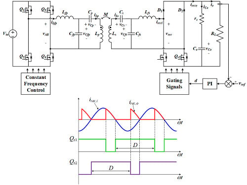
2. IPT System with S-BAR

2.1. System Description

Figure 1 shows a double-sided LCC compensation topology with an S-BAR. This topology includes a full-bridge inverter, a resonant network, and an S-BAR. The full-bridge inverter consists of a DC input source Vin and main switches Q1Q4. The resonance network has symmetrical primary and secondary circuits and consists of one compensation inductor and two compensation capacitors. The semi-bridgeless rectifier consists of upper diodes D1 and D2 and lower switches Qs1 and Qs2. This topology has multiple resonant frequencies, which are defined as follows [10].
L f p C f p = 1 ω o 2 L f s C f s = 1 ω o 2 ( L p L f p ) C p = 1 ω o 2 ( L s L f s ) C s = 1 ω o 2
where Lp and Ls are the self-inductances of the transmitter and receiver coils, respectively, Lfp and Lfs are the primary and secondary series compensation inductors, respectively, Cp and Cs are the primary and secondary series compensation capacitors, respectively, Cfp and Cfs are the primary and secondary parallel compensation capacitors, respectively, and ω o denotes the resonant frequency.
In this paper, to simplify the analysis, with the exception of the equivalent series resistance of the output capacitor, the parasitics are ignored, and all of the devices are assumed to be ideal. In addition, using fundamental harmonic approximation (FHA), all of the harmonics are ignored, and the operating frequency of all the switches is fixed at a resonant frequency. For the double-sided LCC compensation topology, the transmitter coil current iLp is independent of the load resistor RL and mutual inductance M at a resonant frequency. In addition, Lp and Cp do not affect the magnitude of iLp. Therefore, the secondary equivalent circuit, in which the primary circuit is replaced with the induced voltage vsec, can be represented as shown in Figure 2. By Faraday’s law, vsec can be expressed as follows [28].
v s e c = ω s M I L p sin ( ω s t )
where ωs is the switching frequency and ILp is the peak value of the transmitter coil current.

2.2. Operation Principle

Figure 3 and Figure 4 show the key waveforms of the double-sided LCC compensation topology with the S-BAR and the equivalent circuit for each mode, respectively. The operating frequency of main switches Q1Q4 and rectifier switches Qs1 and Qs2 are fixed at the resonant frequency. Qs1 and Qs2 operate with a phase difference of 180° from each other and modulate the amounts of current flowing to the load when ireci has positive and negative directions, respectively. In order for the S-BAR to operate normally, it is assumed that the duty ratio of Qs1 and Qs2 is always greater than 0.5. The operation of this topology can be divided into four modes.
Mode 1 [t0 < t < t1]: At t0, the gate signal of Qs2 is applied, and ireci flowing in the positive direction no longer flows to D2. During this mode, ireci circulates through Qs1 and Qs2, and no energy is transferred to the load. Therefore, rectifier input voltage vrec and rectifier output current ireco are zero, and the energy charged in the output capacitor is supplied to the load.
Mode 2 [t1 < t < t2]: At t1, Qs1 is turned OFF, and ireci flows to the load through D1 and Qs2. vrec is equal to the output voltage and ireco is equal to ireci. The energy is transferred to the load. This mode ends when the direction of ireci changes to the negative direction.
Because the operation principle of Mode 3 and Mode 4 is similar to that of Mode 1 and Mode 2, the detailed descriptions of these will be omitted.

3. Proposed Modeling

In this section, the modeling method for the IPT system with the S-BAR is discussed in detail. The EDF is obtained considering the duty ratio variation of the rectifier switches, and the large-signal and small-signal equivalent models are obtained using the proposed modeling.

3.1. Nonlinear State Equations

The nonlinear state equations are obtained by applying Kirchhoff’s voltage and current laws to the secondary side equivalent circuit in Figure 2, as follows:
v s e c = L s d i L s ( t ) d t + v C s ( t ) + v C f s ( t )
v C f s ( t ) = L f s d i L f s ( t ) d t + v r e c ( t )
i L s ( t ) = C s d v C s ( t ) d t
i L s ( t ) i L f s ( t ) = C f s d v C f s ( t ) d t
i r e c o ( t ) = ( 1 + r c R L ) C o d v C o ( t ) d t + 1 R L v C o ( t )
v o ( t ) = r c R L R L + r c i r e c o ( t ) + R L R L + r c v C o ( t ) .
Equations (3)–(8) are nonlinear state equations that include both nonlinear and linear components.

3.2. Harmonic Approximation

Because it is assumed that all of the switches operate at a resonant frequency, the harmonics of compensation inductor currents and compensation capacitor voltages are greatly attenuated. Therefore, the resonant currents and voltages are quasi-sinusoidal. By applying harmonic approximation, these components can be approximated by the sum of the sine and cosine components as follows
{ v C s ( t ) = v C s , s ( t ) sin ω s t + v C s , c ( t ) cos ω s t v C f s ( t ) = v C f s , s ( t ) sin ω s t + v C f s , c ( t ) cos ω s t
{ i L s ( t ) = i L s , s ( t ) sin ω s t + i L s , c ( t ) cos ω s t i r e c i ( t ) = i r e c i , s ( t ) sin ω s t + i r e c i , c ( t ) cos ω s t
where the subscripts s and c represent the sine and cosine components, respectively. The derivatives of Equations (9) and (10) are calculated as follows:
{ d v C s ( t ) d t = ( d v C s , s ( t ) d t ω s v C s , c ( t ) ) sin ω s t + ( d v C s , c ( t ) d t + ω s v C s , s ( t ) ) cos ω s t d v C f s ( t ) d t = ( d v C f s , s ( t ) d t ω s v C f s , c ( t ) ) sin ω s t + ( d v C f s , c ( t ) d t + ω s v C f s , s ( t ) ) cos ω s t
{ d i L s ( t ) d t = ( d i L s , s ( t ) d t ω s i L s , c ( t ) ) sin ω s t + ( d i L s , c ( t ) d t + ω s i L s , s ( t ) ) cos ω s t d i r e c i ( t ) d t = ( d i r e c i , s ( t ) d t ω s i r e c i , c ( t ) ) sin ω s t + ( d i r e c i , c ( t ) d t + ω s i r e c i , s ( t ) ) cos ω s t .
In Equations (9)–(12), the coefficients of the sine and cosine components change over time and their modulation frequency is much lower than the switching frequency. Thus, these parameters include the dynamics of the resonant network.

3.3. Extended Describing Functions

By applying a harmonic approximation, the quasi-sinusoidal components of Equations (3)–(8) are approximated as sinusoidal components. However, nonlinear components such as rectifier input voltage vrec and rectifier output current ireco still complicate the dynamic analysis. Using the EDF, the nonlinear components can be approximated to their fundamental harmonic and DC components.
As shown in Figure 5, when ireco flows, the magnitude of rectifier input voltage vrec is equal to output voltage vo and the direction of vrec is the same as that of ireci. Because vrec is nonlinear but periodic, it can be approximated using a Fourier series expansion. By ignoring the harmonic components, vrec can be expressed as
v r e c ( t ) = f 1 ( i r e c i , s , i r e c i , c , v C o , d ) sin ω s t + f 2 ( i r e c i , s , i r e c i , c , v C o , d ) cos ω s t
where f1 and f2 are the EDFs of the sine and cosine components, respectively, and can be calculated as follows
f 1 ( i r e c i , s , i r e c i , c , v C o , d ) = 2 v C o π { i r e c i , s i r e c i ( 1 cos ( 2 π d ) ) i r e c i , c i r e c i sin ( 2 π d ) }
f 2 ( i r e c i , s , i r e c i , c , v C o , d ) = 2 v C o π { i r e c i , s i r e c i sin ( 2 π d ) + i r e c i , c i r e c i ( 1 cos ( 2 π d ) ) }
where ireci is given by
i r e c i 2 = i r e c i , s 2 + i r e c i , c 2 .
As can be seen in Figure 5, ireco is a nonlinear and periodic function. Using a Fourier series expansion, ireco can be approximated as
i r e c o ( t ) = f 3 ( i r e c i , s , i r e c i , c , d ) = i r e c i π ( 1 cos ( 2 π d ) )
where f3 is the average rectifier output current.

3.4. Harmonic Balance

By harmonic approximation and the EDF, quasi-sinusoidal components are approximated as their fundamental components, and nonlinear components are approximated as their fundamental and DC components. Substituting Equations (9)–(13) and (17) into Equations (3)–(8), nonlinear state equations can be expressed as the sine, cosine, and DC components as follows:
v s e c , s = L s d i L s , s d t L s ω s i L s , c + v C s , s + v C f s , s
0 = L s d i L s , c d t + L s ω s i L s , s + v C s , c + v C f s , c
v C f s , s = L f s d i L f s , s d t L f s ω s i L f s , c + 2 v C o π { i r e c i , s i r e c i ( 1 cos ( 2 π d ) ) i r e c i , c i r e c i sin ( 2 π d ) }
v C f s , c = L f s d i L f s , c d t + L f s ω s i L f s , s + 2 v C o π { i r e c i , s i r e c i sin ( 2 π d ) + i r e c i , c i r e c i ( 1 cos ( 2 π d ) ) }
i L s , s = C s d v C s , s d t C s ω s v C s , c
i L s , c = C s d v C s , c d t + C s ω s v C s , s
i L s , s i L f s , s = C f s d v C f s , s d t C f s ω s v C f s , c
i L s , c i L f s , c = C f s d v C f s , c d t + C f s ω s v C f s , s
i r e c i π ( 1 cos ( 2 π d ) ) = ( 1 + r c R L ) C o d v C o d t + 1 R L v C o
v o = r c R L i r e c i π ( R L + r c ) ( 1 cos ( 2 π d ) ) + R L R L + r c v C o .
Assuming that the modulation frequency of the switching frequency and duty ratio is much lower than the switching frequency, Equations (18)–(27) can be defined by a nonlinear large-signal model, and Figure 6 shows the nonlinear large-signal equivalent circuit.

3.5. Steady-State Solution

The large-signal model includes both steady-state and transient information. At steady-state quiescent points, the state variables do not change with time. Therefore, a steady-state solution can be obtained by substituting zero for the derivatives of Equations (18)–(27), as follows
A s s X s s = U s s
A s s = [ 0 L s Ω s 1 0 0 0 1 0 L s Ω s 0 0 1 0 0 0 1 0 0 0 0 K 1 K 2 K 1 K 3 + L f s Ω s 1 0 0 0 0 0 K 1 K 3 L f s Ω s K 1 K 2 0 1 1 0 0 C s Ω s 0 0 0 0 0 1 C s Ω s 0 0 0 0 0 1 0 0 0 1 0 0 C f s Ω s 0 1 0 0 0 1 C f s Ω s 0 ]
X s s = [ I L s , s I L s , c V C s , s V C s , c I r e c i , s I r e c i , c V C f s , s V C f s , c ] T
U s s = [ Ω s M I L p 0 0 0 0 0 0 0 ] T
where ωsn is the normalized switching frequency, and K1K3 are given in Appendix A.

3.6. Perturbation and Linearization of Large-Signal Model

The average state variable and input variable near the steady-state quiescent point can be expressed as
x = X + x ^
where the capital letter refers to the nominal value, and the hat “^” indicates the small-signal variables.
Substituting Equation (32) into Equations (18)–(27) and using the partial differentiation to linearize the nonlinear large-signal model, a linearized small-signal model is obtained [33]. The state-space representations of a linearized small-signal model can be derived as follows
{ d x ^ d t = A x ^ + B u ^ y ^ = C x ^ + D u ^
A = [ 0 Ω s 1 / L s 0 0 0 1 / L s 0 0 Ω s 0 0 1 / L s 0 0 0 1 / L s 0 1 / C s 0 0 Ω s 0 0 0 0 0 0 1 / C s Ω s 0 0 0 0 0 0 0 0 0 0 K 4 K 5 K 6 + K 7 + Ω s 1 / L f s 0 K 8 + K 9 0 0 0 0 K 7 K 10 Ω s K 5 K 11 0 1 / L f s K 12 K 13 1 / C f s 0 0 0 1 / C f s 0 0 Ω s 0 0 1 / C f s 0 0 0 1 / C f s Ω s 0 0 0 0 0 0 K 14 K 15 0 0 K 16 ]
B = [ Ω o ( I L s , c + M I L 1 L s ) 0 Ω o I L s , s 0 Ω o V C s , c 0 Ω o V C s , s 0 Ω o I L f s , c K 17 + K 18 Ω o I L f s , s K 19 K 20 Ω o V C f s , c 0 Ω o V C f s , s 0 0 K 21 ]
C = [ 0 0 0 0 K 22 K 23 0 0 K 24 ]
D = [ 0 K 25 ]
x ^ = [ i ^ L s , s i ^ L s , c v ^ C s , s v ^ C s , c i ^ r e c i , s i ^ r e c i , c v ^ C f s , s v ^ C f s , c v ^ C o ] T
u ^ = [ ω ^ s n d ^ ] T
y ^ = [ v ^ o ]
where K4K25 are given in Appendix A.
Figure 7 shows the linearized equivalent circuit of the double-sided LCC compensation topology with the S-BAR. The major control-to-output transfer functions are the switching frequency-to-output voltage transfer function Gvf(s) and duty ratio-to-output voltage transfer function Gvd(s). Because the switching frequency of all the switches is fixed at the resonance frequency by an assumption, a detailed description of Gvf(s) is omitted. Gvd(s) can be derived in two ways. One is to use a linearized equivalent circuit. In the linearized equivalent circuit of Figure 7, Gvd(s) can be derived by setting ωsn to zero. The other method is to use a state-space model, where Gvd(s) can be calculated as follows:
G v d ( s ) = v ^ o d ^ = C ( s I A ) 1 B + D .
Using MATLAB commands, sys = ss(A,B,C,D) and Gvd(s) = tf(sys), Equation (41) can be obtained.

4. Controller Design

Figure 8 shows a block diagram of the output voltage control, where Gc is the output voltage controller, Fm is the PWM gain, and Hvo is the voltage sensor gain. Figure 9 shows the duty ratio-to-output voltage transfer function under various load conditions. The main parameters are presented in Table 1. For stable output voltage control under various load conditions, the worst case condition is selected. In general, a lower frequency for the dominant pole makes it more difficult to obtain a sufficient phase margin. At a 10% load condition, the duty ratio-to-output voltage transfer function has the lowest dominant pole. Therefore, a 10% load condition is selected as the worst case, and the controller is designed at this operating point.
Figure 10 shows the gain and phase plots of the loop gain with and without the controller under the worst case condition. The following PI controller is used for the voltage controller:
G v d ( s ) = 43 1 + 0.0025 s s .
As can be seen in Figure 10, the crossover frequency is 1550 Hz, and the phase margin is 88.5 degree.

5. Experimental Results

5.1. Test Setup

To verify the effectiveness of the proposed modeling method, a double-sided LCC compensation topology with an S-BAR was designed for 100 W, input voltage of 150 V, and output voltage rating of 25 V, as shown in Figure 11. The circuit of the test setup is shown in Figure 1, and the circuit parameters are provided in Table 1. The structures of the transmitter and receiver coils were the same, and each had a length and width of 200 mm and 220 mm, respectively. Each coil consisted of 11 turns of litz wire and 8 ferrite cores. The air gap between the transmitter and receiver coils was 100 mm, and the coupling coefficient was 0.175.

5.2. Verification of Steady-State Performance

Figure 12 shows a comparison of the output voltage curves according to the duty ratio under various load conditions. In Figure 12, the dashed line indicates the calculated output voltage of the proposed model, and the solid line indicates the values measured in the experiments. When the duty ratio is 0.5, this topology has a constant current output characteristic. Thus, the output voltage increases as the load resistance increases. As the duty ratio of the rectifier switch increases, the rectifier output current decreases, and the output voltage decreases. As can be seen in Figure 12, when RL has values of 6.25 Ω and 12.5 Ω, the measured values fit well with the calculated output voltage of the steady-state model. However, when the load resistance is 62.5 Ω, the experimental values do not match well with the calculated values. This is because, when the output voltage is higher than the input voltage, an interval occurs in which the rectifier does not conduct [10]. Therefore, the harmonic components of rectifier input current ireci increase, which causes an error between the values calculated using the model based on the harmonic approximation and the experimental result.

5.3. Transient Response Results

To demonstrate the performance of the controller designed in Section 4, the experimental results of the step response and load change response are provided. Figure 13 represents the experimental results of the step response when reference voltage vref changes from 25 to 30 V under a 100% load condition. Output voltage vo follows its reference voltage without overshoot and the settling time of the step response is approximately 4 ms. Figure 14 shows the steady-state waveforms before and after the step response. As can be seen from these waveforms, the rectifier voltage is zero while the rectifier input current circulates, and the magnitude of vrec is equal to the output voltage when the rectifier output current flows into the load. Therefore, when the reference voltage is 30 V, the zero voltage interval of vrec is shorter to improve the output voltage.
Figure 15 shows the transient response under a load change. When the load varies from 100 W to 10 W, the output voltage follows its reference voltage. During the transient response, the overshoot of the output voltage is approximately 2.5 V, which is 10% of the reference voltage. Figure 16 shows the steady-state waveforms before and after the load change. As described in Section 5.2, the output voltage increases when the load resistance decreases. Therefore, the zero voltage interval of the rectifier voltage is longer to reduce the rectifier output current under the 10 W load condition.

6. Conclusions

This paper proposed a modeling method for a double-sided LCC compensation topology with an S-BAR. Unlike the conventional modeling methods for S-BARs, the proposed modeling reflects the dynamics of the resonant network and S-BAR. It is possible to design a voltage controller with good performance. A detailed mathematical analysis of the proposed modeling method was provided, as well as a nonlinear large-signal model, steady-state solution, and linearized small-signal model. Nonlinear large-signal equivalent circuit and linearized small-signal equivalent circuit are presented for intuitive understanding. The duty ratio-to-output voltage transfer function was obtained from the linearized small-signal model and the controller design procedure considering the worst case condition was discussed. A 100 W prototype was used to demonstrate the effectiveness of the proposed modeling. The steady-state model was verified by the output voltage curves according to the duty ratio of the rectifier switches. At the rated load and medium load, the experimental results fit well with the steady-state model. However, under light load condition, the error between the experimental results and calculated results increased due to harmonic components not considered. The linearized small-signal model was verified using the experimental waveforms of the step response and load change response. The designed controller performance was verified by step response. Through load change response, the designed controller was verified to be robust against load variation.

Author Contributions

Conceptualization, H.-R.C., R.-Y.K. and Y.-J.C.; Formal analysis, H.-R.C. and K.-H.P.; Investigation, H.-R.C. and Y.-J.C.; Methodology, H.-R.C.; Project administration, R.-Y.K. and Y.-J.C.; Software, H.-R.C. and K.-H.P.; Supervision, R.-Y.K. and Y.-J.C.; Validation, H.-R.C.; Visualization, H.-R.C. and R.-Y.K.; Writing—original draft, H.-R.C.; Writing—review & editing, H.-R.C., R.-Y.K., K.-H.P. and Y.-J.C.

Funding

This work was supported by “Human Resources Program in Energy Technology” of the Korea Institute of Energy Technology Evaluation and Planning (KETEP), granted financial resource from the Ministry of Trade, Industry & Energy, Republic of Korea (No. 20171210201100, No. 20184010201710).

Conflicts of Interest

The authors declare no conflict of interest.

Appendix A

K 1 = 2 R L π 2 ( 1 cos ( 2 π D ) )
K 2 = 1 cos ( 2 π D )
K 3 = sin ( 2 π D )
K 4 = 2 V C o I L f s , c 2 π L f s I L f s 3 ( 1 cos ( 2 π D ) )
K 5 = 2 V C o I L f s , s I L f s , c π L f s I L f s 3 sin ( 2 π D )
K 6 = 2 V C o I L f s , s I L f s , c π L f s I L f s 3 ( 1 cos ( 2 π D ) )
K 7 = 2 V C o I L f s , s 2 π L f s I L f s 3 sin ( 2 π D )
K 8 = 2 I L f s , s π L f s I L f s ( 1 cos ( 2 π D ) )
K 9 = 2 I L f s , c π L f s I L f s sin ( 2 π D )
K 10 = 2 V C o I L f s , c 2 π L f s I L f s 3 sin ( 2 π D )
K 11 = 2 V C o I L f s , s 2 π L f s I L f s 3 ( 1 cos ( 2 π D ) )
K 12 = 2 I L f s , s π L f s I L f s sin ( 2 π D )
K 13 = 2 I L f s , c π L f s I L f s ( 1 cos ( 2 π D ) )
K 14 = R L π ( R L + r c ) C o I L f s , s I L f s ( 1 cos ( 2 π D ) )
K 15 = R L π ( R L + r c ) C o I L f s , c I L f s ( 1 cos ( 2 π D ) )
K 16 = 1 ( R L + r c ) C o
K 17 = 4 V C o I L f s , s L f s I L f s sin ( 2 π D )
K 18 = 4 V C o I L f s , c L f s I L f s cos ( 2 π D )
K 19 = 4 V C o I L f s , s L f s I L f s cos ( 2 π D )
K 20 = 4 V C o I L f s , c L f s I L f s sin ( 2 π D )
K 21 = 2 R L I L f s ( R L + r c ) C o sin ( 2 π D )
K 22 = r c R L π ( R L + r c ) I L f s , s I L f s ( 1 cos ( 2 π D ) )
K 23 = r c R L π ( R L + r c ) I L f s , c I L f s ( 1 cos ( 2 π D ) )
K 24 = R L R L + r c
K 25 = 2 r c R L I L f s ( R L + r c ) sin ( 2 π D )

References

  1. Li, S.; Mi, C.C. Wireless power transfer for electric vehicle applications. IEEE J. Emerg. Sel. Top. Power Electron. 2015, 3, 4–17. [Google Scholar]
  2. Covic, G.A.; Boys, J.T. Inductive power transfer. Proc. IEEE 2013, 101, 1276–1289. [Google Scholar] [CrossRef]
  3. Dai, J.; Ludois, D.C. A survey of wireless power transfer and a critical comparison of inductive and capacitive coupling for small gap applications. IEEE Trans. Power Electron. 2015, 30, 6017–6029. [Google Scholar] [CrossRef]
  4. Keeling, N.A.; Covic, G.A.; Boys, J.T. A unity-power-factor IPT pickup for high-power applications. IEEE Trans. Ind. Electron. 2010, 57, 744–751. [Google Scholar] [CrossRef]
  5. Zhang, W.; Wong, S.C.; Chi, K.T.; Chen, Q. Design for efficiency optimization and voltage controllability of series–series compensated inductive power transfer systems. IEEE Trans. Power Electron. 2014, 29, 191–200. [Google Scholar] [CrossRef]
  6. Zhang, W.; Wong, S.C.; Chi, K.T.; Chen, Q. Analysis and comparison of secondary series-and parallel-compensated inductive power transfer systems operating for optimal efficiency and load-independent voltage-transfer ratio. IEEE Trans. Power Electron. 2014, 29, 2979–2990. [Google Scholar] [CrossRef]
  7. Sohn, Y.H.; Choi, B.H.; Lee, E.S.; Lim, G.C.; Cho, G.-H.; Rim, C.T. General unified analyses of two-capacitor inductive power transfer systems: Equivalence of current-source SS and SP compensations. IEEE Trans. Power Electron. 2015, 30, 6030–6045. [Google Scholar] [CrossRef]
  8. Zhang, W.; Mi, C.C. Compensation topologies of high-power wireless power transfer systems. IEEE Trans. Veh. Technol. 2016, 65, 4768–4778. [Google Scholar] [CrossRef]
  9. Wang, C.-S.; Stielau, O.H.; Covic, G. Design considerations for a contactless electric vehicle battery charger. IEEE Trans. Ind. Electron. 2005, 52, 1308–1314. [Google Scholar] [CrossRef]
  10. Li, S.; Li, W.; Deng, J.; Nguyen, T.D.; Mi, C.C. A double-sided LCC compensation network and its tuning method for wireless power transfer. IEEE Trans. Veh. Technol. 2015, 64, 2261–2273. [Google Scholar] [CrossRef]
  11. Li, W.; Zhao, H.; Deng, J.; Li, S.; Mi, C.C. Comparison study on SS and double-sided LCC compensation topologies for EV/PHEV wireless chargers. IEEE Trans. Veh. Technol. 2016, 65, 4429–4439. [Google Scholar] [CrossRef]
  12. Liu, X.; Clare, L.; Yuan, X.; Wang, C.; Liu, J. A Design Method for Making an LCC Compensation Two-Coil Wireless Power Transfer System More Energy Efficient Than an SS Counterpart. Energies 2017, 10, 1346. [Google Scholar] [CrossRef]
  13. Lu, S.; Deng, X.; Shu, W.; Wei, X.; Li, S. A New ZVS Tuning Method for Double-Sided LCC Compensated Wireless Power Transfer System. Energies 2018, 11, 307. [Google Scholar]
  14. Deng, J.; Li, W.; Nguyen, T.D.; Li, S.; Mi, C.C. Compact and efficient bipolar coupler for wireless power chargers: Design and analysis. IEEE Trans. Power Electron. 2015, 30, 6130–6140. [Google Scholar] [CrossRef]
  15. Qu, X.; Chu, H.; Wong, S.-C.; Chi, K.T. An IPT Battery Charger With Near Unity Power Factor and Load-Independent Constant Output Combating Design Constraints of Input Voltage and Transformer Parameters. IEEE Trans. Power Electron. 2019, 34, 7719–7727. [Google Scholar] [CrossRef]
  16. Vu, V.-B.; Tran, D.-H.; Choi, W. Implementation of the constant current and constant voltage charge of inductive power transfer systems with the double-sided LCC compensation topology for electric vehicle battery charge applications. IEEE Trans. Power Electron. 2018, 33, 7398–7410. [Google Scholar] [CrossRef]
  17. Khalilian, M.; Guglielmi, P. Primary-Side Control of a Wireless Power Transfer System with Double-Sided LCC Compensation Topology for Electric Vehicle Battery Charging. In Proceedings of the 2018 IEEE International Telecommunications Energy Conference (INTELEC), Turin, Italy, 7–11 October 2018; pp. 1–6. [Google Scholar]
  18. Zhao, Q.; Wang, A.; Liu, J.; Wang, X. The Load Estimation and Power Tracking Integrated Control Strategy for Dual-Sides Controlled LCC Compensated Wireless Charging System. IEEE Access 2019, 7, 75749–75761. [Google Scholar] [CrossRef]
  19. Vu, V.-B.; Phan, V.-T.; Dahidah, M.; Pickert, V. Multiple Output Inductive Charger for Electric Vehicles. IEEE Trans. Power Electron. 2019, 34, 7350–7368. [Google Scholar] [CrossRef]
  20. Li, B.; Lu, J.-H.; Li, W.-J.; Zhu, G.-R. Realization of CC and CV Mode in IPT System Based on the Switching of Doublesided LCC and LCC-S Compensation Network. In Proceedings of the 2016 International Conference on Industrial Informatics-Computing Technology, Intelligent Technology, Industrial Information Integration (ICIICII), Wuhan, China, 3–4 December 2016; pp. 364–367. [Google Scholar]
  21. Pang, B.; Deng, J.; Liu, P.; Wang, Z. Secondary-side power control method for double-side LCC compensation topology in wireless EV charger application. In Proceedings of the IECON 2017–43rd Annual Conference of the IEEE Industrial Electronics Society, Beijing, China, 29 October–1 November 2017; pp. 7860–7865. [Google Scholar]
  22. Huang, C.-Y.; Boys, J.T.; Covic, G.A. LCL pickup circulating current controller for inductive power transfer systems. IEEE Trans. Power Electron. 2013, 28, 2081–2093. [Google Scholar] [CrossRef]
  23. Diekhans, T.; De Doncker, R.W. A dual-side controlled inductive power transfer system optimized for large coupling factor variations and partial load. IEEE Trans. Power Electron. 2015, 30, 6320–6328. [Google Scholar] [CrossRef]
  24. Kim, M.; Joo, D.-M.; Lee, B.K. High efficient power conversion circuit for inductive power transfer charger in electric vehicles. In Proceedings of the 2017 IEEE 3rd International Future Energy Electronics Conference and ECCE Asia (IFEEC 2017-ECCE Asia), Kaohsiung, Taiwan, 3–7 June 2017; pp. 25–29. [Google Scholar]
  25. Zou, S.; Onar, O.C.; Galigekere, V.; Pries, J.; Su, G.-J.; Khaligh, A. Secondary Active Rectifier Control Scheme for a Wireless Power Transfer System with Double-Sided LCC Compensation Topology. In Proceedings of the IECON 2018–44th Annual Conference of the IEEE Industrial Electronics Society, Washington, DC, USA, 21–23 October 2018; pp. 2145–2150. [Google Scholar]
  26. Mishima, T.; Morita, E. High-frequency bridgeless rectifier based ZVS multiresonant converter for inductive power transfer featuring high-voltage GaN-HFET. IEEE Trans. Ind. Electron. 2017, 64, 9155–9164. [Google Scholar] [CrossRef]
  27. Fan, M.; Shi, L.; Yin, Z.; Li, Y. A novel pulse density modulation with semi-bridgeless active rectifier in inductive power transfer system for rail vehicle. CES Trans. Electr. Mach. Syst. 2017, 1, 397–404. [Google Scholar]
  28. Fan, M.; Shi, L.; Yin, Z.; Jiang, L.; Zhang, F. Improved Pulse Density Modulation for Semi-bridgeless Active Rectifier in Inductive Power Transfer System. IEEE Trans. Power Electron. 2019, 34, 5893–5902. [Google Scholar] [CrossRef]
  29. Colak, K.; Asa, E.; Bojarski, M.; Czarkowski, D.; Onar, O.C. A novel phase-shift control of semibridgeless active rectifier for wireless power transfer. IEEE Trans. Power Electron. 2015, 30, 6288–6297. [Google Scholar] [CrossRef]
  30. Ann, S.; Son, W.-J.; Byun, J.; Lee, J.H.; Lee, B.K. Switch Design for a High-Speed Switching Semi-Bridgeless Active Rectifier of Inductive Power Transfer Systems Considering Reverse Recovery Phenomenon. In Proceedings of the 2019 10th International Conference on Power Electronics and ECCE Asia (ICPE 2019–ECCE Asia), Busan, Korea, 27–30 May 2019; pp. 1–6. [Google Scholar]
  31. Zhao, F.; Zhu, C.; Lu, R.; Song, K.; Wei, G. Modeling and design of control loop with semi-bridgeless rectifier in wireless charging system. In Proceedings of the 2017 IEEE Transportation Electrification Conference and Expo, Asia-Pacific (ITEC Asia–Pacific), Harbin, China, 7–10 August 2017; pp. 1–6. [Google Scholar]
  32. Cha, H.-R.; Park, K.-H.; Choi, Y.-J.; Kim, R.-Y. Double-Sided LCC Compensation Topology with Semi-Bridgeless Rectifier for Wireless Power Transfer System. In Proceedings of the 2019 10th International Conference on Power Electronics and ECCE Asia (ICPE 2019–ECCE Asia), Busan, Korea, 27–30 May 2019; pp. 1–6. [Google Scholar]
  33. Choi, Y.-J.; Cha, H.-R.; Jung, S.-M.; Kim, R.-Y. An Integrated Current-Voltage Compensator Design Method for Stable Constant Voltage and Current Source Operation of LLC Resonant Converters. Energies 2018, 11, 1325. [Google Scholar] [CrossRef]
Figure 1. Double-sided Inductor-Capacitor-Capacitor (LCC) compensation topology with S-BAR.
Energies 12 03921 g001
Figure 2. Secondary side equivalent circuit of double-sided LCC compensation topology with S-BAR.
Energies 12 03921 g002
Figure 3. Key waveforms of double-sided LCC compensation topology with S-BAR.
Energies 12 03921 g003
Figure 4. Equivalent circuits for each mode: (a) Mode 1; (b) Mode 2; (c) Mode 3; (d) Mode 4.
Energies 12 03921 g004
Figure 5. Rectifier voltage and current waveforms according to duty ratio.
Energies 12 03921 g005
Figure 6. Nonlinear large-signal equivalent circuit.
Energies 12 03921 g006
Figure 7. Linearized small-signal equivalent circuit of double-sided LCC compensation topology with S-BAR.
Energies 12 03921 g007
Figure 8. Block diagram of output voltage control.
Energies 12 03921 g008
Figure 9. Open loop bode plot of duty ratio-to-output voltage transfer function under various load conditions.
Energies 12 03921 g009
Figure 10. Gain and phase plots of loop gain with and without controller under worst case condition.
Energies 12 03921 g010
Figure 11. Experimental setup.
Energies 12 03921 g011
Figure 12. Output voltage versus duty ratio under various load conditions.
Energies 12 03921 g012
Figure 13. Step response when voltage reference is changed from 25 to 30 V at 100% load condition.
Energies 12 03921 g013
Figure 14. Experimental waveforms under 100% load condition: (a) Vref = 25 V; (b) Vref = 30 V.
Energies 12 03921 g014
Figure 15. Transient response under load step from 100 W to 10 W.
Energies 12 03921 g015
Figure 16. Experimental waveforms when voltage reference is 25 V: (a) Po = 100 W; (b) Po = 10 W.
Energies 12 03921 g016
Table 1. System specifications and circuit parameters.
ParameterValue (Unit)
Nominal input voltage (Vin)150 (V)
Output power (Po)100 (W)
Output voltage (Vin)25 (V)
Self-inductance of transmitter coil (Lp)48 (μH)
Self-inductance of receiver coil (Ls)48 (μH)
Primary side series compensation inductor (Lfp)18.2 (μH)
Secondary side series compensation inductor (Lfs)18.2 (μH)
Primary side series compensation capacitor (Cp)110 (nF)
Secondary side series compensation capacitor (Cs)110 (nF)
Primary side parallel compensation capacitor (Cfp)180 (nF)
Secondary side parallel compensation capacitor (Cfs)180 (nF)
Coupling coefficient (k)0.175
Resonant frequency (fo)88 (kHz)
Output capacitor (Co)100 (μF)
ESR of output capacitor (rc)1 (mΩ)
Load resistance (RL)6.25–62.5 (Ω)

