Article

An Integrated Design Approach for LCL-Type Inverter to Improve Its Adaptation in Weak Grid

1
State Grid Henan Electric Power Research Institute, Zhengzhou 450052, China
2
State Grid Zhengzhou Electric Power Supply Company, Zhengzhou 450052, China
3
State Key Laboratory of Power Transmission Equipment & System Security and New Technology, Chongqing University, Chongqing 400044, China
*
Author to whom correspondence should be addressed.
Energies 2019, 12(13), 2637; https://doi.org/10.3390/en12132637
Submission received: 16 May 2019 / Revised: 2 July 2019 / Accepted: 2 July 2019 / Published: 9 July 2019

Abstract

:
To improve the robustness of grid-connected inverter against grid impedance in a weak grid an integrated design method of LCL-filter parameters and controller parameters is proposed. In the method the inherent relation of LCL-filter parameters and controller parameters is taken into consideration to realize their optimized match. A parameter normalization scheme is also developed to facilitate the system stability and robustness analysis. Based on the method all normalization parameters can be designed succinctly according to the required stability and robustness. Additionally, the LCL parameter and controller parameter can be achieved immediately by restoring normalization parameters. The proposed design method can guarantee the inverter stability and robustness simultaneously without needing any compensation network, additional hardware, or the complicated iterative computations which cannot be avoided for the conventional inverter design method. Simulation and experiment results have validated the superiority of the proposed inverter design method.

1. Introduction

LCL-type inverters have been widely utilized in renewable energy applications to convert DC power into AC power [1,2] as renewable energy expands. One of the challenges encountered by grid-connected inverters is the instability due to the uncertainty and variation grid impedance in a weak grid [3,4,5,6]. It has been revealed that the interaction between inverter and grid impedance is the main reason for that problem [7,8,9,10]. Additionally, some solutions have been proposed to cope with this issue from different perspectives. The existing solutions for this problem can be classified as two categories. One is to add additional compensation network in the inverter or hardware equipment outside the inverter after the instability phenomenon occurs in the power plant [11,12,13,14,15,16,17,18,19,20,21,22]. Additionally, the other is the optimization design by taking grid impedance into account before the inverter is produced [23,24,25,26,27,28,29,30].
The first class of methods belongs to repair strategies. For example, a zero-compensation element is inserted in the conventional current controller to improve the phase response [11]. An online phase compensation method was proposed to ensure that the inverter has enough stability margins and bandwidth against varied grid impedance [12]. The notch filter was designed to generate an anti-resonance peak to offset the resonance of the LCL filter [13,14]. Since LCL resonant frequency varies along with grid impedance, the center frequency of the notch filter has to be regulated from the detected resonance frequency in real time. Given that the feedforward of the voltage at the point of common coupling (PCC) is equivalent to adding a virtual impedance in parallel with the inverter output impedance [15,16,17,18], possible solutions are to enhance the phase margin by reshaping the magnitude or phase of the ratio of the inverter output impedance and the grid impedance. Based on the feedforward PCC voltage, the grid current feedback has been used through the estimated grid impedance to alleviate the influence of grid impedance on system stability [19]. Reference [20] proposed an optimized capacitor-current-feedback active damping to improve inverter robustness against grid impedance. Additional equivalent impedance is added to the LCL filter in [21] to enhance the inverter robustness in a weak grid. A rectifier connected to the PCC was controlled as an active damper to damp the resonance [22]. Since this kind of method needs additional compensation networks or hardware devices it is complicated in practice.
The second class of methods is to take the grid impedance into consideration while the inverter is designed originally. A controller parameter design guideline based on the current loop transfer function was proposed to obtain better system performance against grid impedance variation [23]. An optimal capacitor-current-feedback for a digitally-controlled inverter was investigated so that the gain margin for stability was always satisfied as grid impedance varies [24]. A robust active damping factor and current controller parameters were designed to ensure that the inverter stability margins satisfy the requirement as grid impedance varies from the minimum to the maximum value [25]. Two stability criteria were proposed to limit the controller parameters [26]. Then collection of controller parameters fulfilling the criteria is derived so that the inverter can function well in a weak grid. Others attempt to improve the inverter robustness by the advanced controller [27,28]. The robust partial state feedback [27] and a robust H∞ controller [28] have been employed in the single-loop inverter to improve the inverter adaptability to grid impedance. An optimized range of the ratio between the switching frequency and resonant frequency was derived to ensure that the active damping is always effective under the grid impedance variation [29]. Moreover, the ratio between the grid-side inductance and the converter-side inductance was optimized to reduce the influence of LCL parameter variation on resonant frequency. An LCL-filter parameter design method was developed to ensure the resonant frequency always in the tolerance range as LCL-filter parameter variation due to the internal and external factors [30]. Although this kind of method can prevent instabilities for grid-connected inverters to some degree, it always designs LCL parameters and controller parameters separately rather than taking their inherent relation into consideration. Therefore, this kind of method cannot realize the optimal match between LCL parameters and controller parameters to prevent instabilities.
In fact, the stability and robustness of the grid-connected inverter are closely related to the LCL parameters as well as the controller parameters. Only when LCL parameters and controller parameters complement each other perfectly will the inverter be characterized with strong stability and robustness. Therefore, the paper is aimed at developing a robust inverter design method by taking the inherent relation of LCL parameters and controller parameters into consideration. Additionally, the salient contributions are summarized as follows: (1) An integrated inverter design method by taking the inherent relation of LCL-filter parameters and controller parameters into consideration is proposed; (2) A parameter normalization scheme is developed to facilitate the system stability and robustness analysis; (3) Parameter constraints and design guidelines for robust inverter design are derived.
The rest of this paper is organized as follows. In Section 2, the inverter is modeled and stability constraints are investigated. Section 3 derives the limitations of control parameters such that the current loop transfer function and the inverter admittance contain no RHP poles. The proposed integrated design method is described in Section 4. Section 5 presents a case study to illustrate the design procedure. Simulation and experimental results are presented in Section 6. Section 7 states the conclusion.

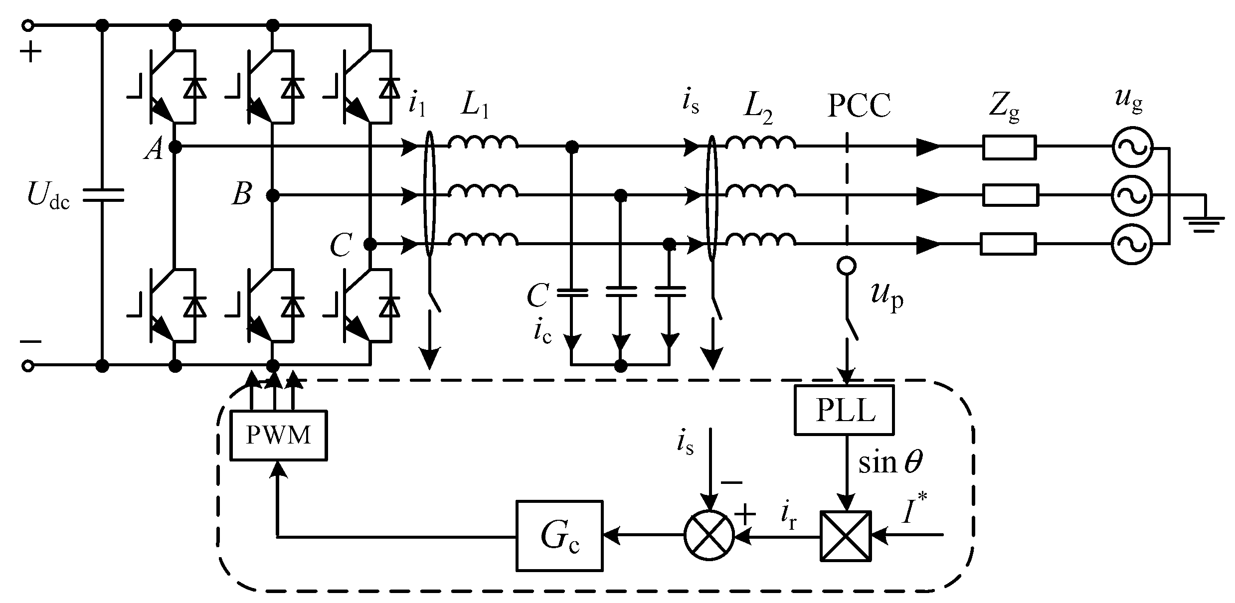
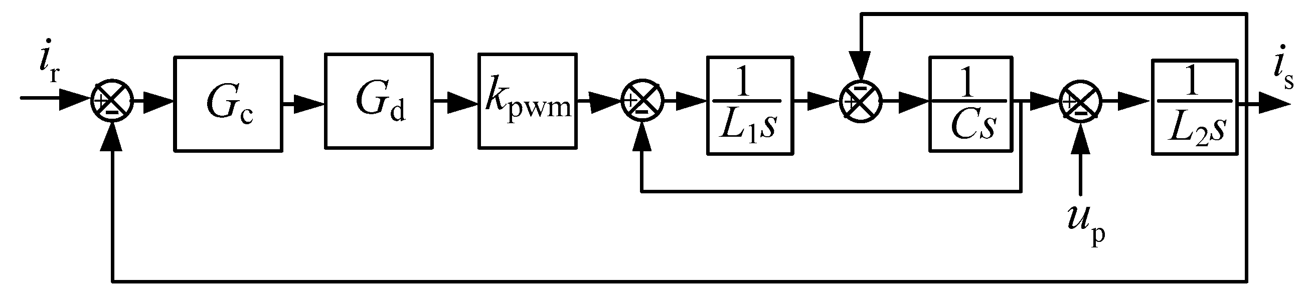
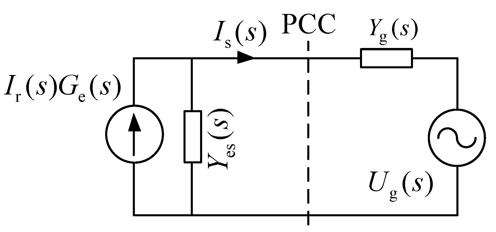
2. System Modeling and Stability Constraint

Single loop control structure of the LCL-inverter with grid-side current feedback is shown in Figure 1. L1 is the inverter-side filter inductance, L2 the grid-side inductance, and C is the filter capacitor. Udc is the dc-link voltage. i1 is the inverter-side current and is is the inverter current to the grid. ic is the filter capacitor current and up is the PCC voltage. Zg is the grid impedance and ug is the ideal power grid voltage. In the control structure, ir is the reference current generated by the magnitude of I* and the PCC phase locked by PLL. Gc is the quasi-proportional plus resonant (quasi-PR) current controller [23]
G c ( s ) = k p + 2 k r ω i s s 2 + 2 ω i s + ( ω 0 ) 2
where kp is the proportional coefficient, kr is the resonant coefficient, ωi is the bandwidth coefficient, and ω0 is the fundamental angular frequency.
The s-domain model of the inverter is depicted in Figure 2 where kpwm Udc/2 is the transfer function of the pulse width modulation (PWM) modulator and Gd(s) is the transfer function of the total delay due to digital control. The delay includes the computation delay, zero-order holder and the sampling switch and can be expressed as [31]
G d ( s ) = 1 T s 1 e T s s s e T s s
According to Figure 2, the open-loop transfer function from the current (ir is) to is is to be derived as
G os ( s ) = i s i r i s = k pwm G c ( s ) G d ( s ) s 3 L 1 L 2 C + s ( L 1 + L 2 )
and the inverter admittance can be expressed as
Y es ( s ) = i s u p = s 2 L 1 C + 1 s 3 L 1 L 2 C + s ( L 1 + L 2 ) + k pwm G c G d
The Norton model of the inverter is depicted in Figure 3 [15]. Yg is the equivalent grid admittance and Ug the grid voltage. Ge is the closed-loop transfer function from the reference current to the inverter output current and can be expressed
G e ( s ) = G os ( s ) G os ( s ) + 1
It has been shown [32] that stability of the system in Figure 3 can be assessed by the admittance ratio Ko = Yes/Yg as long as Ge contains no RHP (right-half plane) poles. If Gos satisfies the Nyquist criterion, then Ge contains no RHP poles. In accordance to Nyquist criterion, more conditions have to be satisfied to guarantee the closed-loop system stable if the open-loop transfer function contains RHP poles. If Gos contains RHP poles, sufficient stability margin is difficult to obtain even though Gos satisfies the Nyquist criterion [24]. The inverter design method developed in the following will be based on the condition that Gos contains no RHP poles.
Yg does not contain any RHP poles or RHP zeros because it is passive. So the admittance ratio Ko has no RHP poles as long as Yes does not contain any RHP poles. Additionally, the system will be stable as long as Ko has sufficient phase margin (PM). For the grid impedance, since the resistive part tends to make the system stable, in this study, only the inductive component is considered. Therefore, Yg = 1/(sLg), where Lg is equivalent grid inductance. The phase of Yg can be viewed as −90° for all frequencies. Then the PM of Ko can be expressed as
PM = 180 ° | arg [ Y es ( j ω in ) ] + 90 ° |
where ωin denotes the frequency at which the magnitude responses of Yes and Yg intersect. Generally, PM should be no less than 30° to thwart the adverse effects due to harmonics [16]. Therefore, arg[Yes(in)] should be in the range of (−240°, 60°). However ωin varies with the variation of Lg. To keep PM > 30° as Lg varies, the phase response of Yes is required to be in the range of (−240°, 60°). Therefore, one of the design objectives is to keep the phase arg[Yes()] in (−240°, 60°) for a wide frequency range.

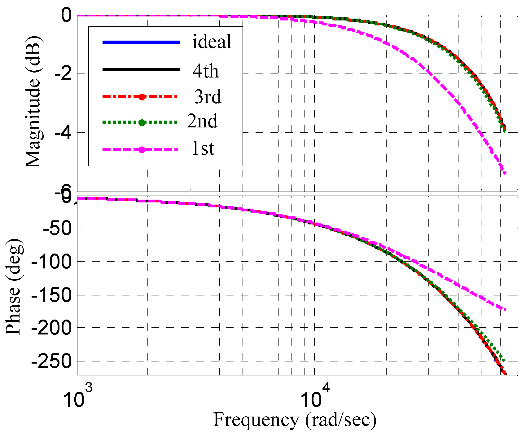
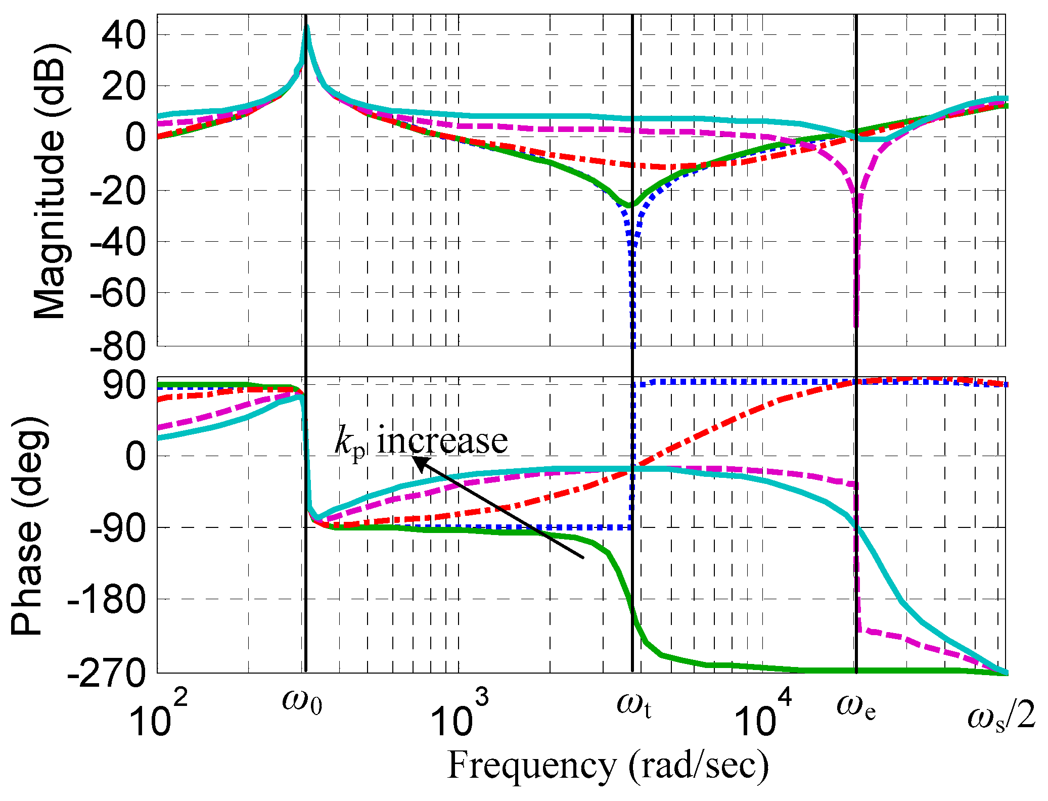
3. Frequency Response Analysis

This section develops alternative expressions of the inverter admittance so that the frequency response can be easily analyzed for stability improvement. Instead of using the admittance, we investigate the frequency response of the impedance. It follows from Equation (4) that the inverter impedance can be expressed as
Z es = s L 2 + 1 s 2 L 1 C + 1 Z c 1 ( s L 1 + k pwm G c G d ) Z a = Z 2 + Z c 1 Z a Z cs
It can be seen from Equation (7) that Zes is expressed as two impedances: Z2 the impedance due to the grid-side filter inductance and Zcs = Zc1 · Za the equivalent impedance seen from the filter capacitor, i.e., Z cs = u c / i s .
Since Zes is the reciprocal of Yes, it follows from (6) that the phase of Zes should be in the range of (−60°, 240°) in order to keep PM of Ko no less than 30°. It is desired that Yes contains no RHP poles. Then Zes should contain no RHP zero. Since Z2 does not contain any RHP zero or RHP pole, if Zcs has no RHP zero or RHP pole, then Zes does not have any RHP zero.
The Padé approximation is widely adopted to linearize Gos and Za because they are nonlinear functions [31]. Figure 4 shows the frequency responses of the first-order to the fourth-order Padé approximations and the original function. It can be seen from Figure 4 that the fourth-order approximation is sufficiently accurate for a broad range of frequencies. Therefore, in the following the fourth-order approximation is brought in to conduct the qualitative analysis, such as obtaining the variation tendency of root locus zeros or Bode diagrams. Meanwhile, Euler’s equation is brought in to conduct the quantitative analysis such as obtaining the boundary value of kp.
The following is to find the range of kp such that Zcs contains no RHP zeros. Since the zeros of Zcs are the same as that of Za, and it is easier to find kp from Za, Za is used to conduct the analysis.
Figure 5 illustrates the zero locus of Za with a fourth-order Padé approximation. Additionally, there are 15 zeros in Za. It is observed from Figure 5 that two crossover points occur at the imaginary axis. One appears when moving from RHP to the left-half plane (LHP), another from LHP to the RHP.
Figure 6 shows the Bode diagrams of Za for various kp. It is observed from Figure 6 that two resonant peaks occur at ωt and ωe no matter what the value of kp is. This implies that |Za()| is nearly zero at ωt or ωe. To find ωe, we assume that ωe is much larger than ω0 such that kr is ignored. Then the frequency response Za(e) can be expressed as
Z a ( j ω e ) = k pwm k p B j ( k pwm k p A ω e 2 L 1 ) ω e
where A = cos T s ω cos 2 T s ω T s , B = sin 2 T s ω sin T s ω T s , Ts is the sampling period.
Set the real part of Za(e) to zero. We have kp = 0 or B = 0. When kp = 0, the imaginary part of Za(e) is not zero. Therefore kp = 0 does not make |Za(e)| = 0. Since B = 0 occurs at ω = ωs/6, then the imaginary part of Za(e) becomes zero at ωe = ωs/6 and kp = kpcr where
k pcr = ω s 2 L 1 T s 36 k pwm .
To find ωt, kr cannot be ignored because ωt is close to ω0. Under this circumstance, the real part and the imaginary part of Za(t) are expressed as
{ Re [ Z a ( j ω t ) ] = [ A J D k r + B J 2 k p + B D 2 ( k p + k r ) ] k pwm ( J 2 + D 2 ) ω t Im [ Z a ( j ω t ) ] = ω t L 1 [ A J 2 k p + A D 2 ( k p + k r ) J D B k r ] k pwm ( J 2 + D 2 ) ω t
where J = ω 0 2 ω t 2 and D = 2 ω i ω t .
By setting Re{Za(t)} = 0 and Im{Za(t)} = 0, the solution yields the relationship between kr and ωt
( J 2 + D 2 ) ω t 2 L 1 B + ( B 2 + A 2 ) D J k pwm k r = 0 .
Combining Re{Za(t)} = 0 with equation (11), we obtain the lower bound of kp as
k pt = k r D ( 3 ω t T s J + 2 D ) 2 ( J 2 + D 2 ) .
It is concluded from Equations equation (9) and (12) that the range of kp that ensures Za does not have RHP zero is kpt kp kpcr.
Moreover, it can be derived from Equation (10) that the phase of Za(t) can be expressed as
φ ( ω t ) = 3 ω t T s 2
It is observed from Figure 6 that when 0 < kp < kpt, all phase curves cross φ(ωt) − 180° at ωt and tend to be −270° at the high-frequency range. When kpt < kp < kpcr, all phase curves cross φ(ωt) at ωt and cross 90° at ωe. For kp > kpcr, all phase curves cross φ(ωt) at ωt and cross −90° at ωe.
In summary, since Zc1 does not contain RHP poles. To guarantee that Yes does not contain any RHP poles, kp should be in the range of (kpt, kpcr).

4. Integrated Design Method

To improve grid-connected inverter robustness to grid impedance, this section presents an integrated design method to design the LCL-filter parameters and inverter controller parameters. The following parameter normalization is used for the development: kp = λpkpcr where kpt/kpcr < λp < 1.

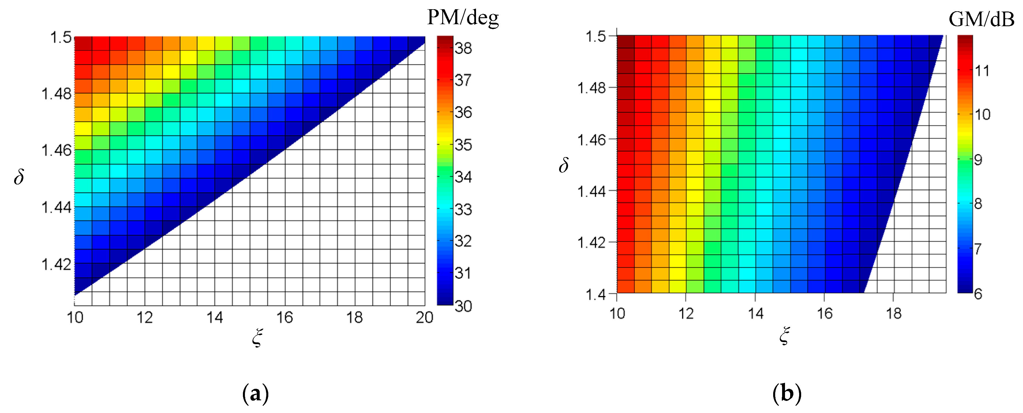
4.1. Design ωres and ωc According to Stability Margin Constraints of Gos

Generally, the cutoff frequency ωc is far away from ω0 to guarantee enough bandwidth. Therefore, the resonant coefficient of the current controller kr can be ignored. On the other hand, the phase curve of Gos crosses 180° at the frequency below ωr. Therefore, to obtain enough stability margins, ωc is usually set much lower than ωr. Therefore, the influence of the filter capacitance C on |Gos(c)| can be neglected. That is to say both kr and C can be neglected when calculating |Gos(c)|. Then kp can be derived as Equation (14) by setting |Gos()| = 1
k p = ω c ( L 1 + L 2 ) k pwm
The open-loop transfer function can be expressed as Equation (15) according to Equation (3).
G os ( s ) = 1 L 1 L 2 C k pwm G c ( s ) G d ( s ) s 3 + s ω res 2
where ω res = L 1 + L 2 L 1 L 2 C .
To normalize ωres and ωc we mark ωres = δωe and ωc = ξω0. To ensure the stability, δ should be larger than 1 and ωc should be lower than ωe, i.e., ξ < ωe/ω0. ωres is generally lower than half of the switching frequency, i.e., ωres < ωsw/2, to ensure the proper filtering performance on the switching harmonics. Since ωsw is equal to ωs/2 for the regular-sampling method, the range of δ is (1, 1.5). ωc should be larger than 10ω0 to obtain sufficient bandwidth. Therefore the feasible range of ξ is (10, ωe/ω0).
Substituting the above normalization parameters into Equation (15) a normalized open-loop transfer function of the single-loop inverter can be derived as
G os ( s ) = ξ δ 2 ω e 2 ω 0 G d ( s ) s 3 + s δ 2 ω e 2
Since ω0, ωe, and Ts are known, Gos can be determined by δ and ξ. Therefore, the inverter stability margins is also dependent on δ and ξ. These normalization parameters and their feasible region are known. Therefore, PM and GM can be analyzed based on the normalized model of Equation (16).
Suppose that the required stability margins are GM > 6dB and PM > 30°. The regions of ξ and δ that meet the stability margin requirements are shown in Figure 7. It is observed from Figure 7 that both GM and PM increase as δ rises. Nevertheless, both GM and PM decrease as ξ rises. It is found that δ = 1.5 is the optimal value such that both GM and PM are the maximum. As can be seen from Figure 7, under this circumstance, ξ should be in (10, 19.4) to guarantee GM > 6 dB and PM > 30°. For sufficient stability margins, ξ should not be set too large. Therefore, care should be taken to select ξ and δ to obtain large stability margins as well as sufficient bandwidth.

4.2. Design ωr1 and kp According to Phase Constraints of Zes

It can be seen from Equation (7) that Zc1 only contains a pair of conjugate poles on imaginary axis. Additionally, a resonant peak appears at ω r 1 = 1 / ( L 1 C ) . In the range (0, ωr1), the phase of Zc1 is zero which does not affect the phase of Zcs. However, Zc1 has a phase jump of −180° at ωr1. When ω > ωr1, the phase of Zc1 becomes −180°. The frequency response of Zcs(s) can be expressed as
Z cs ( j ω ) = ω r 1 2 Z a ( j ω ) ω r 1 2 ω 2
It can be seen from Equation (17) that arg[Zcs()] is the same as arg[Za()] for ω < ωr1. On the other hand, arg[Zcs()] is equal to arg[Za()]−180° for ω > ωr1. Bode diagrams of Zcs(s) for various ωr1 are shown as Figure 8. It is observed from Figure 8 that arg[Zcs()] approaches to −90° even lower than −90° in the vicinity of ωr1. Figure 8 also shows the Bode diagrams of Z2 for different L2. It shows that |Zcs()| is much larger than |Z2()| in the vicinity of ωr1. When ω approaches to ωr1 from the left hand side, arg[Zes(r1)] ≈ arg[Za(r1)] and when ω approaches ωr1 from the right, we have arg[Zes(r1)] ≈ arg[Za(r1)]−180°. To have arg[Zes(r1)] in (−60°, 240°), both arg[Za(r1)] and arg[Za(r1)]−180° should be in (−60°, 240°), that is, arg[Za(r1)] should be in (120°, 240°).
It has been shown in the above analysis that the phase of Zc1 is below 90° in (ω0, ωe), but above 90° in (ωe, ωs/2). The phase curve shifts up with the increase of kp. So ωr1 should be set in (ωe, ωs/2) to make the phase of Za(r1) higher than 120°. Since ωe is much larger than ω0, kr can be neglected when analyzing the frequency characteristic of Za in (ωe, ωs/2). Without considering kr the phase frequency characteristic of Za can be derived as Equation (18). To normalize the phase function, we define ωr1 = βωe where 1 > β > 0. Then arg[Za(r1)] can be obtained as Equation (19) by substituting ω = ωr1 into (18).
arg [ Z a ( j ω ) ] = 180 ° + arctan ( 9 ω 2 T s 2 2 λ p π 2 cos 3 T s ω 2 sin T s ω 2 tan 3 T s ω 2 )
arg [ Z a ( j ω r 1 ) ] = 180 ° + arctan ( β 2 2 λ p cos π β 2 sin β π 6 tan β π 2 ) ,
By combining Equation (9) with Equation (14), λp can be rewritten as Equation (20). Substituting Equation (20) into Equation (19) yields arg[Za(r1)] as Equation (21).
λ p = 36 δ 2 ξ ω 0 ω s 2 T s ( δ 2 β 2 ) .
arg [ Z a ( j ω r 1 ) ] = 180 ° + arctan ( β 2 ω s 2 T s ( δ 2 β 2 ) 72 δ 2 ξ ω 0 cos π β 2 sin π β 6 tan π β 2 ) .
This phase arg[Za(r1)] is a function of β only because ξ and δ have been known. Figure 9 illustrates the relationship of arg[Za(r1)] and β for β in (1, δ). It shows that the phase is a monotonic increasing function of β. The phase arg[Za(r1)] is equal to 120° at β = βs1, which can be obtained by solving the equation arg[Za(r1)] = −120°. Therefore, we have arg[Zes(r1)] 60 ° if β is in (βs1, δ).
In addition, it can be seen from Equation (20) that λp is also a monotonic increasing function of β. There is an upper bound βs2 to make λp = 1. It is derived from Equation (20) that βs2 can be expressed as
β s 2 = δ 1 ξ ω 0 ω e 2 T s .
Therefore, the value of β should be in (βs1, βs2) to have arg[Zes(jωr1)]   60 ° . In addition, since L2 is getting large when β approaches δ, β should be selected as βs1 or the value slightly higher than βs1 so that L2 will not be too large. After β is determined, λp can be obtained according to Equation (20).

4.3. LCL Filter Computation According to Normalization Parameters
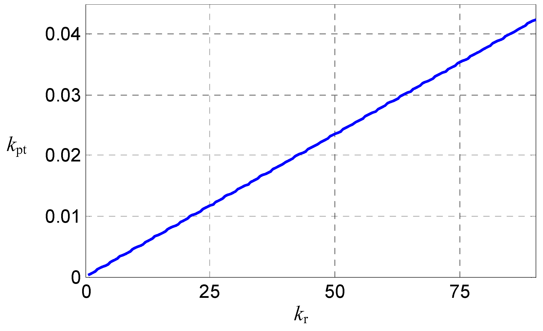
In this part, an LCL filter design scheme is developed by combing ωr1 and ωres with constraints of the switching harmonics on LCL filter. The LCL filter design can be started with the design of converter-side inductance. In the three-phase four-wire system, the maximum current ripple at the inverter output is given by equation [33]
Δ I max = U dc 6 L 1 f sw .
To restrict the switching current and the core loss of L1, the current ripple on the inverter side is recommended to be around 20% of the rated inverter current. Then the inverter-side inductance can be determined by
L 1 U dc 6 × 20 % I s f sw
where I s = 2 P n 3 U g . It is recommended that L1 be selected at or slightly larger than the lower bound in order to keep the cost low and reduce the core loss. It follows from the relation ωr1 = βωe that the capacitance C can be selected by
C = 1 L 1 β 2 ω e 2 .
Moreover, since the reactive power absorbed by the filter capacitance should not be more than 5%, C is limited by
C 5 % P 3 ω 0 U g 2 .
Finally, the grid-side inductance L2 can be derived as Equation (27) from the relation ωres = δωe.
L 2 = 1 C ω e 2 ( δ 2 β 2 )

4.4. Design of kr

It has been shown [23] that |Gos(0)| higher than 50 dB and |Zes(0)| larger than 40 dB would enable the system to have a good tracking performance. If the influence of L2, C, and Gd on |Zes(0)| is negligible, then |Zes(0)| can be expressed as
| Z es ( j ω 0 ) | = ( ω 0 L 1 ) 2 + [ k pwm ( k p + k r ) ] 2 .
Similarly, since C and Gd only have a slight effect on |Go(0)|, ignoring C and Gd yields
| G os ( j ω 0 ) | = k pwm ( k p + k r ) ω 0 ( L 1 + L 2 ) .
If it is required that |Zes(0)| > 40 dB and |Gos(0)| > 50 dB, then kr should satisfy the following condition
k r max { 10 4 ( ω 0 L 1 ) 2 k pwm k p , 10 2.5 ω 0 ( L 1 + L 2 ) k pwm k p } .
Although ωc is far away from ω0, kr still affects the phase of Gos in the controller bandwidth. With the increase of kr, the phase of Gos in the controller bandwidth decreases. This leads to the reduction of stability margins. Therefore, an upper limit krm1 for kr needs to be set to guarantee GM > 6 dB and PM > 30°.
In accordance with Equations (11) and (12), kpt and kr has a positive linear relationship, as shown in Figure 10. Kpt rises as kr increases. Therefore, there is an upper bound krm2 that satisfies kpt < kp. krm2 can be obtained by a numerical method. Therefore, the overall constraint of kr can be obtained by
max { 10 4 ( ω 0 L 1 ) 2 k pwm k p , 10 2.5 ω 0 ( L 1 + L 2 ) k pwm k p } < k r < min { k rm 1 , k rm 2 }

4.5. Detailed Design Procedure

Table 1. summarizes the parameter constraints and design guideline of the integrated design method. Procedure of the design is presented below.
(1)
Initialize the power converter parameters: the rated power Pn, rated ac voltage Ug, fundamental frequency f0, dc-link voltage Udc, sampling frequency fs, and the switching frequency fsw.
(2)
Refer to Figure 7 to obtain stability margins as large as possible. Set δ as 1.5.
(3)
According to Figure 7, ξ should be selected from (10, 19.4) for δ = 1.5 to satisfy the stability margin, PM > 30° and GM > 6 dB. The final ξ should be selected according to the desired stability margins and bandwidth.
(4)
Select β from (βs1, βs2) and β should be close to βs1.
(5)
Compute λp from Equation (20). Select L1 from Equation (24) near the lower bound.
(6)
Calculate C using Equation (25), verify that Equation (26) is satisfied, and obtain L2 from Equation (27).
(7)
Select kr according to Equation (31).
As seen, compared with traditional inverter design method the proposed method is simple and does not need complicated iterative computation and the trial and error method to design LCL filter and controller parameters. Additionally, a set of normalization parameters can be used to design many inverters no matter what the power level is. More importantly, the inverter will be characterized with strong stability and robustness to grid impedance by using the proposed method.

5. Case Study

A 500 kW inverter was considered to evaluate the performance of the proposed integrated design method. In the test, the sampling frequency was 16 kHz. The DC-link voltage and the grid voltage were Udc = 700 V and Ug = 220 V, respectively. The asymmetric regular-sampling method was employed and the switching frequency was 8 kHz. The LCL filter and controller parameters designed by the proposed integrated design method and the conventional method are shown in Table 2. The conventional methods design LCL filter and controller parameters separately and do not consider the inverter impedance [23,34,35,36].

5.1. Parameter Design

(1)
Start with Pn = 500 kW, fs = 16 kHz, Udc = 700 V, Ug = 220 V, and fsw = 8 kHz.
(2)
δ is set as 1.5 in order to have the stability margins as large as possible.
(3)
ξ is set as 15 to obtain enough bandwidth and stability margins.
(4)
According to Equations (21) and (22) the range of β is calculated as (1.23, 1.28). A tradeoff between L2 and λp yields β = 1.23.
(5)
Then λp is calculated as 0.82 and the lower bound of L1 is 68 μH according to Equation (24). L1 is set as 70 μH.
(6)
C is calculated as 33.6μF, which is less than the upper bound of 548 μF from Equation (26) and L2 as 143.7 μH.
(7)
The range of kr is (0.2828, 1.47) obtained by Equation (31). kr is set as 1. Additionally, kp is calculated as 0.0029.

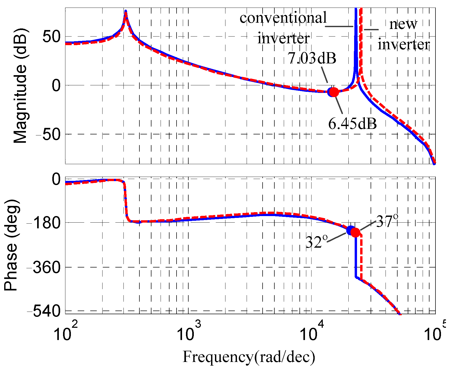
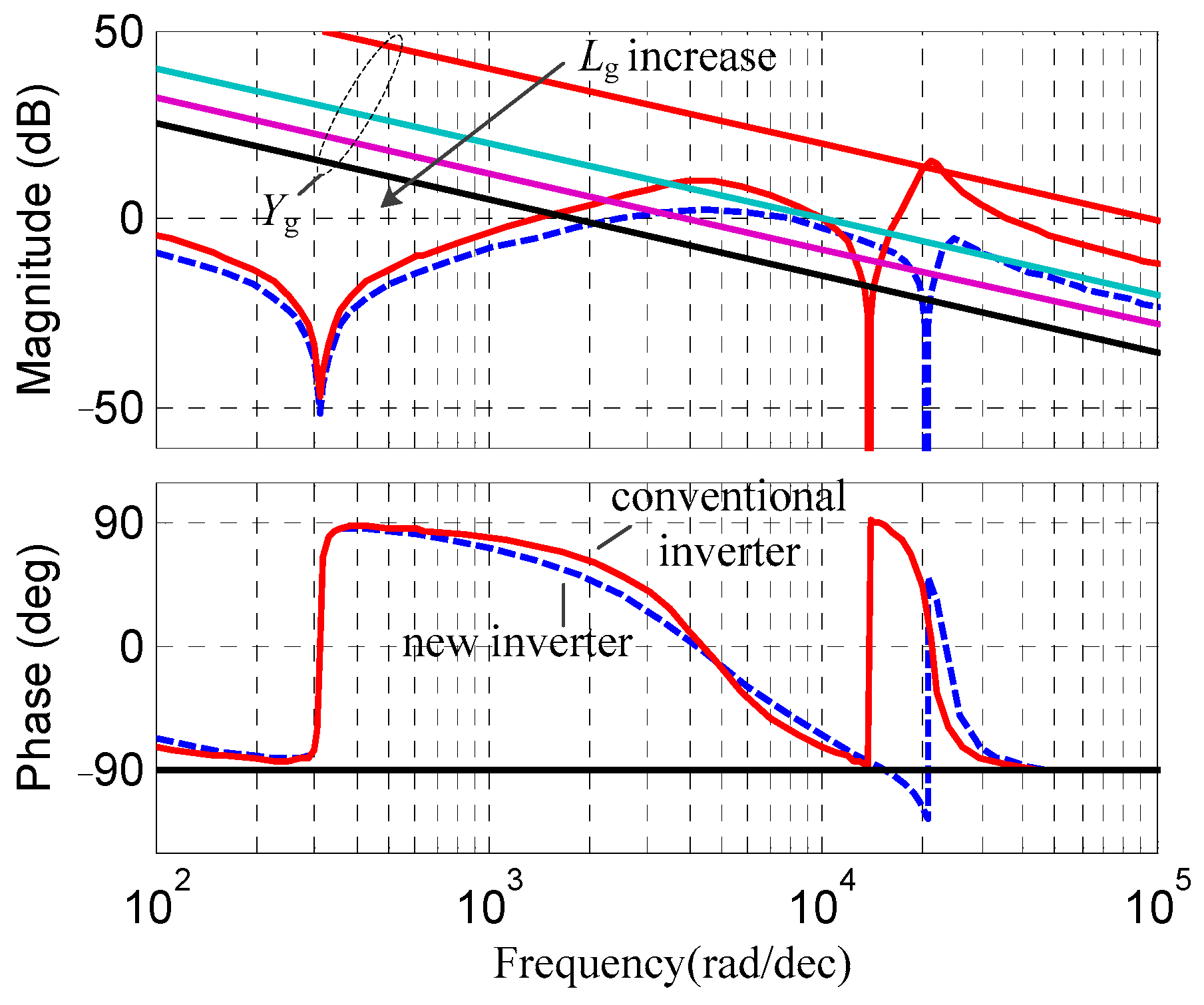
5.2. Performance Evaluation

Bode diagrams of Gos for new and conventional inverters are shown in Figure 11 using the parameters in Table 2. It is observed from Figure 11 that both inverters provide sufficient stability margins. Additionally, the bandwidth is large enough to produce satisfactory dynamic performance.
Bode diagrams of inverter admittance and grid admittance for new and conventional inverters are shown in Figure 12 to evaluate the robustness to grid impedance interaction. It can be seen from Figure 12 that the phase curve of the new inverter admittance is lower than 90° for the whole frequency range. Therefore, the admittance ratio Ko = Ye/Yg satisfies the Nyquist criterion as the grid impedance varies. Close examination reveals that the intersection frequency of the grid admittance and the inverter admittance becomes small as Lg increases. However, the phase difference between the grid and inverter admittance at the intersection frequency is always lower than 150° even for very large Lg. Therefore, the cascade system can obtain sufficient stability margin even though the inverter is connected to a weak grid.
For the conventional inverter, there is a frequency range where the admittance phase exceeds 90°. When the frequency at which the magnitude response of the inverter admittance and that of the grid admittance intersect falls in that frequency band, the PM of Ko = Ye/Yg becomes negative. This indicates that the grid-inverter system loses stability. Since the inverter impedance is not considered in the conventional controller design, even though the current open-loop transfer function is designed with sufficient stability margins, the inverter impedance may exist in the unstable region, where the phase of inverter admittance is larger than 90°.

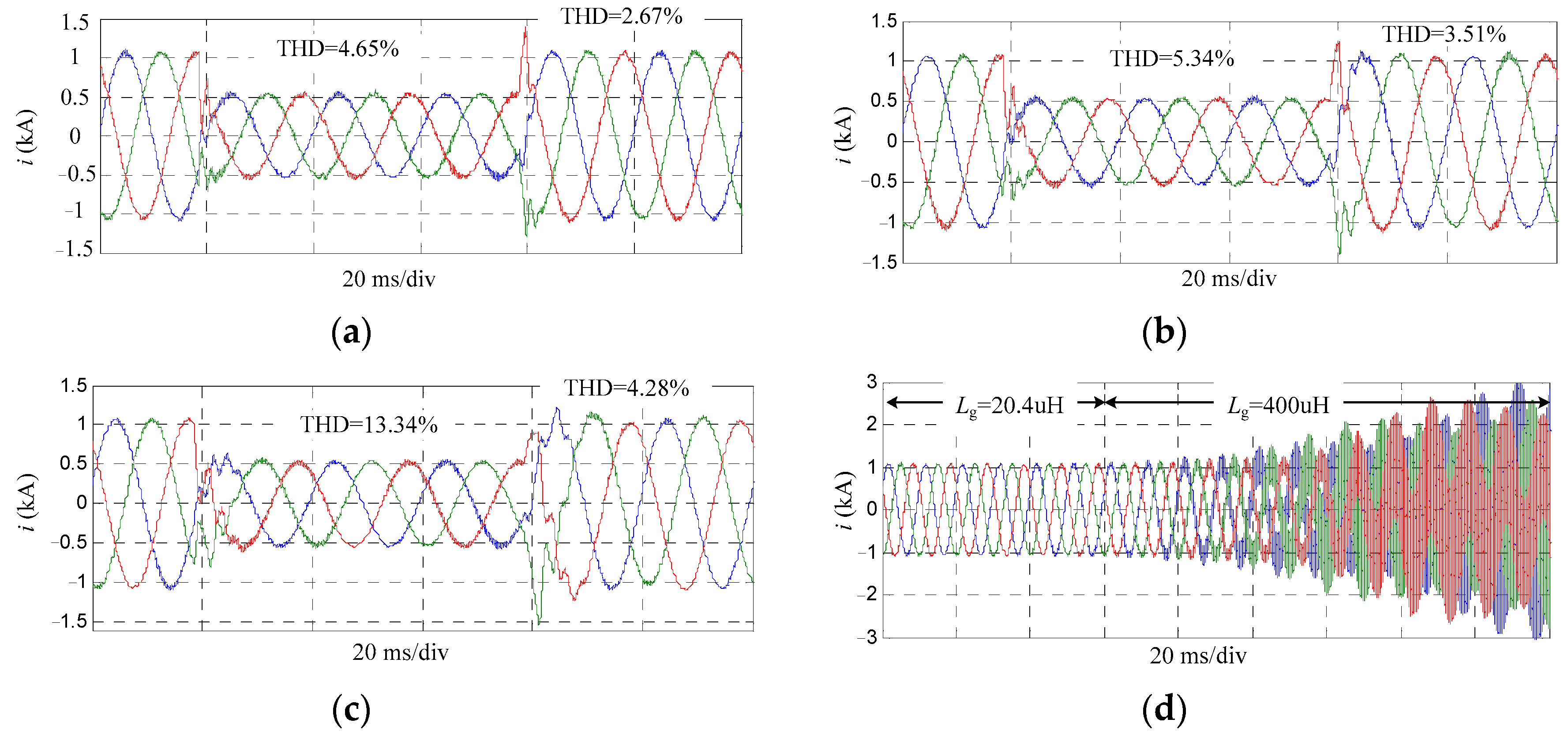
6. Simulation and Experimental Results

Extensive simulations and experiments have been conducted to verify the effectiveness and robustness of the proposed integrated inverter design method in a weak grid.

6.1. Simulation Results

Parameters of the inverter used in the test are listed in Table 2. In MATLAB simulation, both current and voltage signals are sampled by ZOH and the computation delay is emulated by a delay module with one sampling period. To demonstrate the transient performance of the inverter, the reference currents of the current loop are alternated between the full load and half load.
Simulation results of the inverter output currents under different SCRs (Short Circuit Capacity Ratio) for new and conventional inverters are shown as Figure 13 and Figure 14 respectively. Reference currents step between full and half load to illustrate the transient performance. It is evidenced from Figure 13 that the steady-state current is smooth with satisfactory total harmonic distortion (THD). All THDs of the steady-state current are not larger than 2%, which satisfies with the IEEE 519 Std. However, for the conventional inverter, all THDs of the steady-state current are much larger than that of the new inverter. In particular, when Lg is larger than 61μH the THD for half load exceeds 5% which does not meet the IEEE 519 Std. Both inverters exhibit oscillation and overshoot current after the reference current steps. Additionally, the overshoot current of the new inverter is smaller than that of the conventional inverter for large grid impedance. Even worse, when Lg increases to 400 μH, currents of the conventional inverter are completely out of control, indicating that the inverter loses stability.

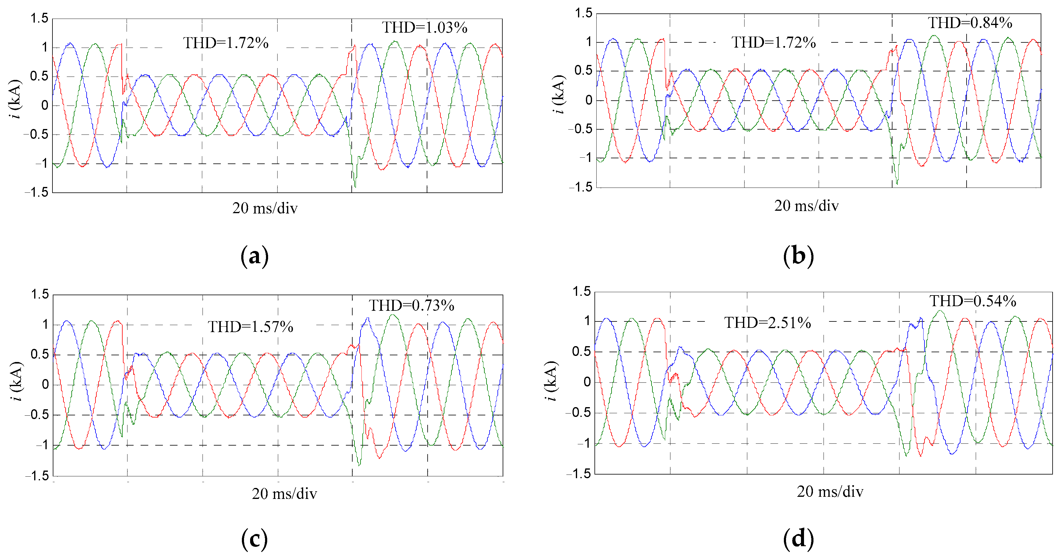
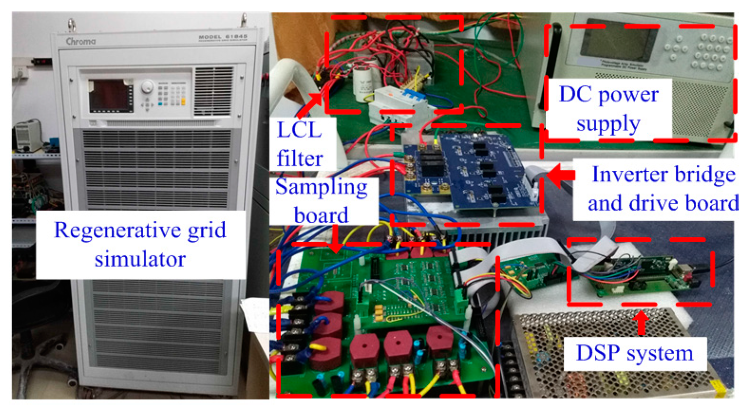
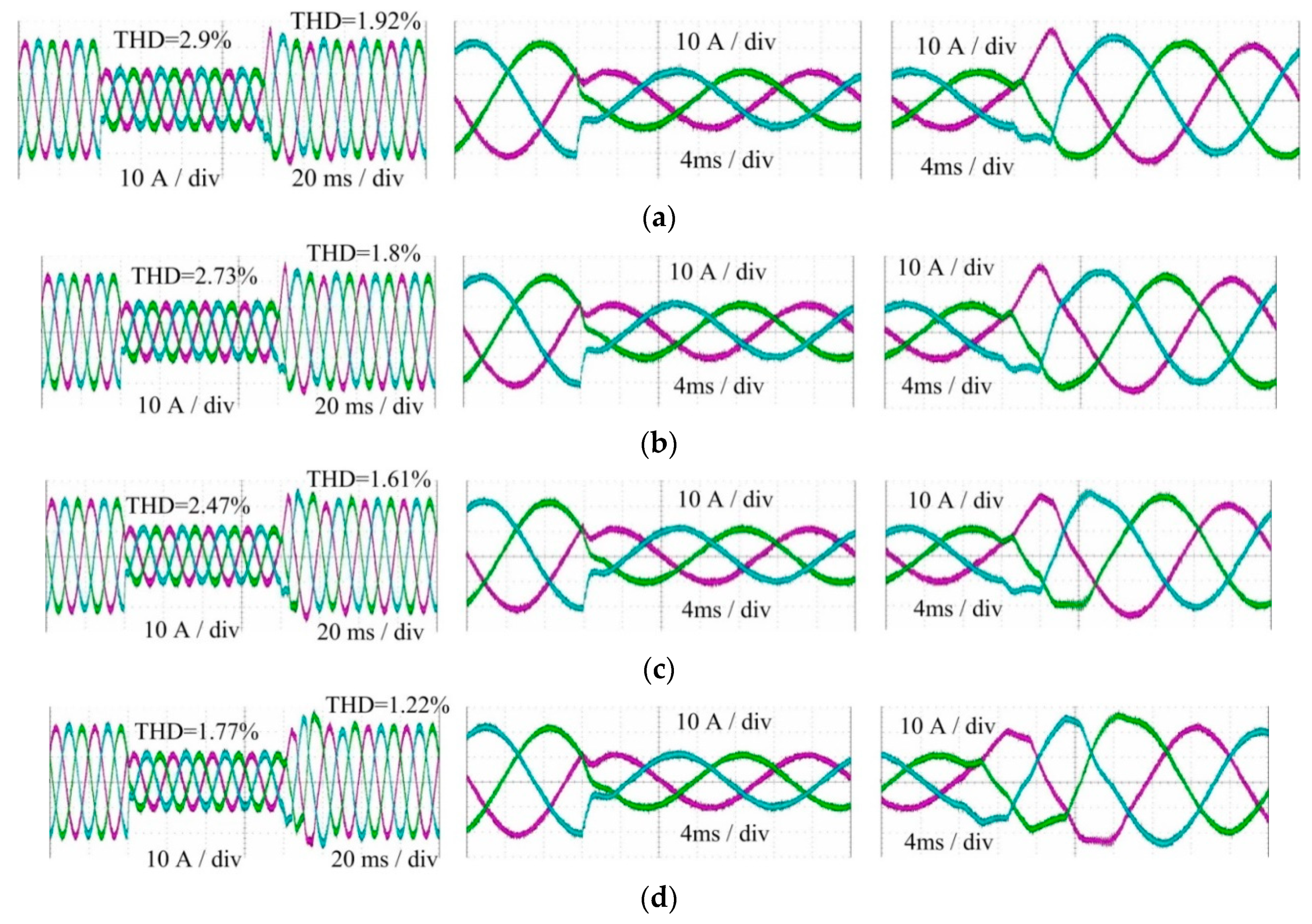
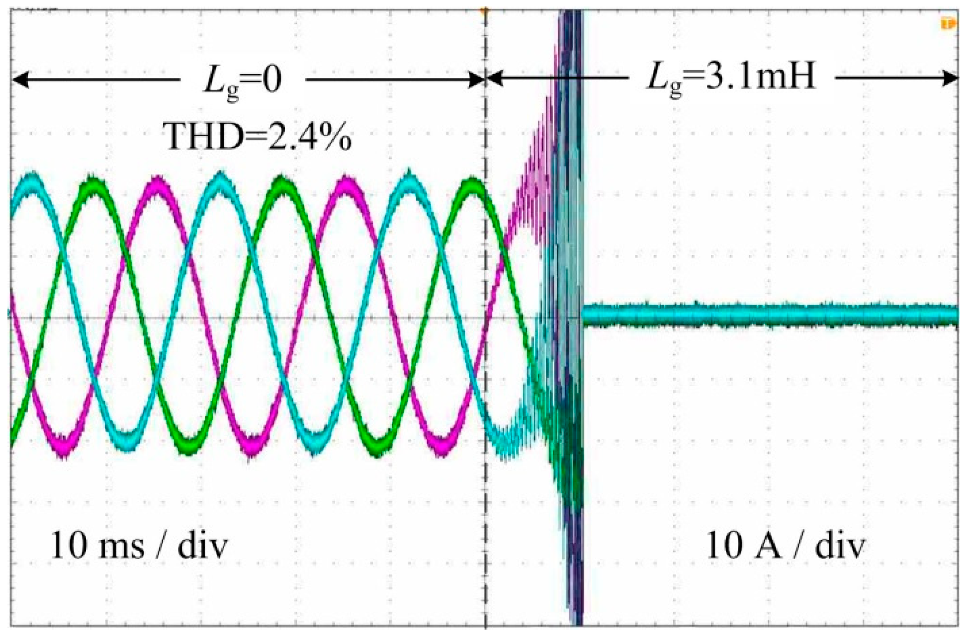
6.2. Experimental Results

Experimental test was conducted to evaluate the effectiveness of the proposed inverter design method. The test is based on a 10 kW experiment setup shown as Figure 15. The three-phase inverter bridge is realized by a CCS050M12CM2 module. The program of the control algorithm for the inverter is generated through a z-domain MATLAB/Simulink model and is implemented in the TMS320F28335 system. In the experiment, an inductor is inserted at the PCC in series with the programmable AC source to emulate the inductive grid impedance. Inverters designed by the proposed methods and the conventional method are shown as Table 3.
Output currents of the new inverter for various SCR are shown in Figure 15. In the figures, the middle panel is the zoom-in view of the left panel showing the step-down detail and the right panel is that of the step-up. It can be seen from Figure 16 that all currents are stable with small THDs in response to load changes. All THDs of the steady-state current are less than 3% satisfied with the IEEE 519 Std. The step-down transients are excellent with nearly no oscillation and no overshoot. Small overshoots appear in the step-up transients. The transient time of the step up is slightly longer than that of the step down. Additionally, longer response time is observed as the grid impedance increases.
Experimental results of such output currents are shown in Figure 17. It can be seen from that the output currents are satisfactory at Lg = 0. A disastrous high-frequency resonance happens when Lg is only increased to 3.1 mH. For protection, the inverter is disconnected to the grid. Simulation and experiment results demonstrate that the proposed integrated design method improves the inverter robustness to grid impedance.

7. Conclusions

This paper has presented an integrated design method that carries out the design of LCL filter and controller by taking their inherent relation into account. This design improves the inverter performance on stability and robustness with respect to grid impedance. A parameter normalization scheme based on parameter constraints has also been developed to facilitate the system stability and robustness analysis. Investigations have shown that the inherent LCL resonant frequency and the cutoff frequency of the current open-loop transfer function are crucial to the inverter stability margins. The proportional factor of the current controller and the resonant frequency of the inverter-side LC filter are critical to the inverter robustness. Procedures that integrate the design of LCL filter and controller parameters have been described. Additionally, parameter constraints and design guidelines for robust inverter design are derived. Simulation and experimental results have demonstrated that the proposed design method improves the inverter robustness to grid impedance, whereas the conventional design methods may fail.

Author Contributions

Conceptualization, C.Z.; methodology, S.L. and Q.L; validation, Y.L. and C.Z.; formal Analysis, S.D.; investigation, C.Z.; writing—original draft preparation, C.Z.; writing—review & editing, Y.T., B.Z. and M.M.

Funding

This research was funded by the China Postdoctoral Science Foundation (2019M652539, 2018M643410), the project “Research on Key Detection Technologies and Propagation Characteristics of Supraharmonics in Power Electronic Distribution Network”, the National Natural Science Foundation of China (grant number 51477021) and the Chongqing Special Postdoctoral Science Foundation (XmT2018033).

Conflicts of Interest

The authors declare no conflict of interest.

References

  1. Carrasco, J.; Franquelo, L.G.; Bialasiewicz, J.; Galvan, E.; PortilloGuisado, R.; Prats, M.; Leon, J.I.; Moreno-Alfonso, N.; Prats, M.A.M. Power-electronic systems for the grid integration of renewable energy sources: A survey. IEEE Trans. Ind. Electron. 2006, 53, 1002–1016. [Google Scholar] [CrossRef]
  2. Blaabjerg, F.; Teodorescu, R.; Liserre, M.; Timbus, A. Overview of control and grid synchronization for distributed power generation systems. IEEE Trans. Ind. Electron. 2006, 53, 1398–1409. [Google Scholar] [CrossRef]
  3. Guan, Y.; Wang, Y.; Xie, Y.; Liang, Y.; Lin, A.; Wang, X. The Dual-Current Control Strategy of Grid-Connected Inverter with LCL Filter. IEEE Trans. Power Electron. 2019, 34, 5940–5952. [Google Scholar] [CrossRef]
  4. Huang, X.; Wang, K.; Fan, B.; Yang, Q.; Li, G.J.; Xie, D.; Crow, M.L. Robust Current Control of Grid-tied Inverters for Renewable Energy Integration under Non-Ideal Grid Conditions. IEEE Trans. Sustain. Energy 2019. [Google Scholar] [CrossRef]
  5. Goh, H.; Armstrong, M.; Zahawi, B. Adaptive control technique for suppression of resonance in grid-connected PV inverters. IET Power Electron. 2019, 12, 1479–1486. [Google Scholar] [CrossRef]
  6. Gulur, S.; Iyer, V.M.; Bhattacharya, S. A Dual Loop Current Control Structure with Improved Disturbance Rejection for Grid Connected Converters. IEEE Trans. Power Electron. 2019, 34, 10233–10244. [Google Scholar] [CrossRef]
  7. Juntunen, R.; Korhonen, J.; Musikka, T.; Smirnova, L.; Pyrhönen, O.; Silventoinen, P. Identification of resonances in parallel connected grid Inverters with LC- and LCL-filters. In Proceedings of the IEEE Applied Power Electronics Conference and Exposition, Charlotte, NC, USA, 15–19 March 2015; pp. 2122–2127. [Google Scholar]
  8. Agorreta, J.L.; Borrega, M.; Lopez, J.; Marroyo, L. Modeling and control of N-paralleled grid-connected inverters with LCL filters coupled due to grid impedance in PV plants. IEEE Trans. Power Electron. 2011, 26, 770–785. [Google Scholar] [CrossRef]
  9. Lu, M.; Wang, X.; Loh, P.C.; Blaabjerg, F. Resonance interaction of multiparallel grid-connected inverters with LCL filter. IEEE Trans. Power Electron. 2017, 32, 894–899. [Google Scholar] [CrossRef]
  10. Yoon, C.; Bai, H.; Beres, R.; Wang, X.; Bak, C.; Blaabjerg, F. Harmonic stability assessment for multiparalleled grid-connected inverters. IEEE Trans. Sustain. Energy 2016, 7, 1388–1396. [Google Scholar] [CrossRef]
  11. Jia, Y.; Zhao, J.; Fu, X. Direct grid current control of LCL-filtered grid-connected inverter mitigating grid voltage disturbance. IEEE Trans. Power Electron. 2014, 29, 1532–1541. [Google Scholar]
  12. Zheng, C.; Zhou, L.; Yu, X.; Li, B.; Liu, J. Online phase margin compensation strategy for a grid-tied inverter to improve its robustness to grid impedance variation. IET Power Electron. 2016, 9, 611–620. [Google Scholar] [CrossRef]
  13. Pena-Alzola, R.; Liserre, M.; Blaabjerg, F.; Ordonez, M.; Kerekes, T. A self-commissioning notch filter for active damping in a three-phase LCL-filter-based grid-tie converter. IEEE Trans. Power Electron. 2014, 29, 6754–6761. [Google Scholar] [CrossRef]
  14. Yao, W.; Yang, Y.; Zhang, X.; Blaabjerg, F.; Loh, P.C. Design and analysis of robust active damping for LCL filters using digital notch filters. IEEE Trans. Power Electron. 2017, 32, 2360–2375. [Google Scholar] [CrossRef]
  15. Yang, D.; Ruan, X.; Wang, H. Impedance shaping of the grid-connected inverter with LCL filter to improve its adaptability to the weak grid condition. IEEE Trans. Power Electron. 2014, 29, 5795–5805. [Google Scholar] [CrossRef]
  16. Chen, X.; Zhang, Y.; Wang, S. Impedance-phased dynamic control method for grid-connected inverters in a weak grid. IEEE Trans. Power Electron. 2017, 32, 274–283. [Google Scholar] [CrossRef]
  17. Céspedes, M.; Sun, J. Impedance shaping of three-phase grid-parallel voltage-source converters. In Proceedings of the IEEE Applied Power Electronics Conference and Exposition (APEC), Orlando, FL, USA, 5–9 February 2012; pp. 754–760. [Google Scholar]
  18. Céspedes, M.; Sun, J. Adaptive control of grid-connected inverters based on online grid impedance measurements. IEEE Trans. Power Electron. 2014, 5, 516–523. [Google Scholar] [CrossRef]
  19. Xu, J.; Xie, S.; Tang, T. Improved control strategy with grid-voltage feedforward for LCL-filter-based inverter connected to weak grid. IET Power Electron. 2014, 7, 2660–2671. [Google Scholar] [CrossRef]
  20. He, Y.; Wang, X.; Ruan, X.; Pan, D.; Xu, X.; Liu, F. Capacitor-Current Proportional-Integral Positive Feedback Active Damping for LCL-Type Grid-Connected Inverter to Achieve High Robustness Against Grid Impedance Variation. IEEE Trans. Power Electron. 2019. [Google Scholar] [CrossRef]
  21. Zhang, Z.; Wu, W.; Shuai, Z.; Wang, X.; Luo, A.; Chung, H.S.-H.; Blaabjerg, F.; Chung, H.S.H. Principle and Robust Impedance-Based Design of Grid-tied Inverter with LLCL-Filter under Wide Variation of Grid-Reactance. IEEE Trans. Power Electron. 2019, 34, 4362–4374. [Google Scholar] [CrossRef]
  22. Wang, X.; Blaabjerg, F.; Liserre, M.; Chen, Z.; He, J.; Li, Y. An active damper for stabilizing power-electronics-based AC systems. IEEE Trans. Power Electron. 2014, 29, 3318–3329. [Google Scholar] [CrossRef]
  23. Bao, C.; Ruan, X.; Wang, X.; Li, W.; Pan, D.; Weng, K. Step-by-step controller design for LCL-type grid-connected inverter with capacitor–current-feedback active-damping. IEEE Trans. Power Electron. 2014, 29, 1239–1253. [Google Scholar]
  24. Pan, D.; Ruan, X.; Bao, C.; Li, W.; Wang, X. Optimized controller design for LCL-type grid-connected inverter to achieve high robustness against grid-impedance variation. IEEE Trans. Ind. Electron. 2015, 62, 1537–1547. [Google Scholar] [CrossRef]
  25. Saïd-Romdhane, M.B.; Naouar, M.W.; Slama-Belkhodja, I.; Monmasson, E. Robust active damping methods for LCL filter-based grid-connected converters. IEEE Trans. Power Electron. 2017, 32, 6739–6750. [Google Scholar] [CrossRef]
  26. Freijedo, F.D.; Rodriguez-Diaz, E.; Golsorkhi, M.S.; Vasquez, J.C.; Guerrero, J.M. A root-locus design methodology derived from the impedance/admittance stability formulation and its application for LCL grid-connected converters in wind turbines. IEEE Trans. Power Electron. 2017, 32, 8218–8228. [Google Scholar] [CrossRef]
  27. Gabe, I.J.; Montagner, V.F.; Pinheiro, H. Design and implementation of a robust current controller for VSI connected to the grid through an LCL filter. IEEE Trans. Power Electron. 2009, 24, 1444–1452. [Google Scholar] [CrossRef]
  28. Kahrobaeian, A.; Mohamed, Y.A.-R.I. Robust single-loop direct current control of LCL-filtered converter-based DG units in grid-connected and autonomous microgrid modes. IEEE Trans. Power Electron. 2014, 29, 5605–5619. [Google Scholar] [CrossRef]
  29. Pena-Alzola, R.; Liserre, M.; Blaabjerg, F.; Ordonez, M.; Yang, Y. LCL-filter design for robust active damping in grid-connected converters. IEEE Trans. Ind. Inf. 2014, 10, 2192–2203. [Google Scholar] [CrossRef]
  30. Wu, T.-F.; Misra, M.; Lin, L.-C.; Hsu, C.-W.; Lin, L.-C. An improved resonant frequency based systematic LCL filter design method for grid-connected inverter. IEEE Trans. Ind. Electron. 2017, 64, 6412–6421. [Google Scholar] [CrossRef]
  31. Buso, S.; Mattavelli, P. Digital Control in Power Electronics; Morgan & Claypool: Seattle, WA, USA, 2006; pp. 17–64. [Google Scholar]
  32. Sun, J. Impedance-based stability criterion for grid-connected inverters. IEEE Trans. Power Electron. 2011, 26, 3075–3078. [Google Scholar] [CrossRef]
  33. Reznik, A.; Simoes, M.G.; Al-Durra, A.; Muyeen, S.M. LCL filter design and performance analysis for grid-Interconnected systems. IEEE Trans. Ind. Appl. 2014, 50, 1225–1232. [Google Scholar] [CrossRef]
  34. Liserre, M.; Blaabjerg, F.; Hansen, S. Design and control of an LCL-filter-based three-phase active rectifier. IEEE Trans. Ind. Appl. 2005, 41, 1281–1291. [Google Scholar] [CrossRef]
  35. Jalili, K.; Bernet, S. Design of LCL filters of active-front-end two level voltage-source converters. IEEE Trans. Ind. Electron. 2009, 56, 1674–1689. [Google Scholar] [CrossRef]
  36. Channegowda, P.; John, V. Filter optimization for grid interactive voltage source inverters. IEEE Trans. Ind. Electron. 2010, 57, 4106–4114. [Google Scholar] [CrossRef]
Figure 1. Control strategy of the grid-connected inverter for grid-side current feedback control structures.
Energies 12 02637 g001
Figure 2. Current control block diagram in s-domain.
Energies 12 02637 g002
Figure 3. System equivalent Norton model.
Energies 12 02637 g003
Figure 4. Frequency responses of Gd with Padé approximations of various orders.
Energies 12 02637 g004
Figure 5. Zero locus of Za as kp varies from 10−4 to 5 × 10⁻³ with a step of 10−5.
Energies 12 02637 g005
Figure 6. Bode diagram of Za for various kp.
Energies 12 02637 g006
Figure 7. Stability margin as a function of ξ and δ: (a) Phase margin, (b) Gain margin.
Energies 12 02637 g007
Figure 8. Bode diagrams of Zcs and Z2.
Energies 12 02637 g008
Figure 9. Relationship of arg[Za(r1)] and β as β varies from 1 to δ.
Energies 12 02637 g009
Figure 10. Relationship of kpt and kr.
Energies 12 02637 g010
Figure 11. Bode diagrams of Gos for new and conventional inverters.
Energies 12 02637 g011
Figure 12. Interaction Bode diagrams between the inverter admittance and grid admittance for new and conventional inverters.
Energies 12 02637 g012
Figure 13. Simulation results of the new inverter for different SCRs. (a) Lg = 20.4 μH (SCR = 45). (b) Lg = 61 μH (SCR = 15). (c) Lg = 184 μmH (SCR = 5). (d) Lg = 460 μH (SCR = 2).
Energies 12 02637 g013
Figure 14. Output currents of the conventional inverter for different SCRs. (a) Lg = 20.4 μH (SCR = 45). (b) Lg = 61 μH (SCR = 15). (c) Lg = 184 μmH (SCR = 5). (d) Lg steps to 400 μH from 20.4 μH.
Energies 12 02637 g014
Figure 15. Photo of the experiment setup.
Energies 12 02637 g015
Figure 16. Current waveforms of the new inverter for various SCR. (a) Lg = 1.0 mH (SCR = 45). (b) Lg = 3.1 mH (SCR = 15). (c) Lg = 9.23.1 mH (SCR = 5). (d) Lg = 23 mH (SCR = 2). Left panel: current waveform; middle panel: zoom-in view of current step down; right panel: zoom-in view of current step up.
Energies 12 02637 g016
Figure 17. Output currents of the conventional inverter with zero and nonzero grid impedance.
Energies 12 02637 g017
Table 1. Parameter Constraint and Design Guideline.
ParameterConstraint Design Guideline
δ, ξRegion shown in Figure 7Consider the desired bandwidth and make PM and GM as large as possible
β(βs1, βs2)β should be close to βs1
λp λ p = 36 δ 2 ξ ω 0 ω s 2 T s ( δ 2 β 2 ) --
L1 L 1 U dc 6 × 20 % I s f sw L1 should be as close to the lower bound as possible
C C = 1 L 1 β 2 ω e 2 C 5 % P 3 ω 0 U g 2
L2 L 2 = 1 C ω e 2 ( δ 2 β 2 ) --
kp k p = λ p ω s 2 L 1 T s 36 k pwm --
kr max { 10 4 ( ω 0 L 1 ) 2 k pwm k p ,   10 2.5 ω 0 ( L 1 + L 2 ) k pwm k p } < k r < min { k rm 1 ,   k rm 2 } kr should be as close to the upper bound as possible
Table 2. New and conventional inverter parameters.
ItemL1 (μH)C (μF)L2 (μH)kpkr
new inverter7033.6143.70.00291
conventional inverter7040750.00140.73
Table 3. New and conventional experiment inverter parameters.
ItemL1 (mH)C (μF)L2 (mH)kpkr
new inverter1.51.04.30.077618
conventional inverter4.02.00.70.0635

