Article

A Composite Strategy for Harmonic Compensation in Standalone Inverter Based on Linear Active Disturbance Rejection Control

1
School of Automation Engineering, Shanghai University of Electric Power, Shanghai 200090, China
2
School of Engineering and Built Environment, Griffith University, Gold Coast, QLD 4222, Australia
*
Author to whom correspondence should be addressed.
Energies 2019, 12(13), 2618; https://doi.org/10.3390/en12132618
Submission received: 6 June 2019 / Revised: 1 July 2019 / Accepted: 4 July 2019 / Published: 8 July 2019

Abstract

:
This paper proposes a harmonic compensation control with disturbance rejection function for a standalone inverter. Due to the LC type three-phase three-leg inverter is connected to nonlinear loads, low-order harmonic components appears in the inverter output current. These harmonic current generate harmonic voltage drops when flowing through the filter inductor and the feeder impedance, which causes the output voltage of the inverter distorted. In order to compensate harmonics and produce sinusoidal voltage without additional compensation devices, virtual harmonic impedance method can be added to the fundamental voltage control. Due to the compensation effect of virtual harmonic impedance are very sensitive to the fluctuation of filter inductance. Therefore, inductance variation, as a disturbance in physical system, should be considered. In this paper, linear active disturbance rejection control (LADRC) is proposed in the fundamental voltage control loop to reduce the sensitivity of virtual harmonic impedance and decouple the model. Compared with traditional dual-loop PI control, the proposed strategy has faster dynamic response in control performance and fewer acquisition modules in engineering applications. The whole design process of virtual harmonic impedance and stability analyses of this strategy are provided. The simulation and experiment results show the good performance of the proposed strategy.

1. Introduction

With the application of distributed energy resources, the penetration rate of renewable energy sources has been greatly increased. While bringing low carbon and economic benefits, intermittency and poor power quality also appear. Therefore, the concept of microgrid is proposed, which combines distributed energy resources with utility grid to effectively overcome these shortcomings [1,2,3]. In order to guarantee the power quality of demand side, many standards have been proposed, especially for harmonic problems. Current harmonic distortion increases the additional losses of electrical equipment, overheating the equipment, reducing equipment efficiency and utilization [4,5,6].
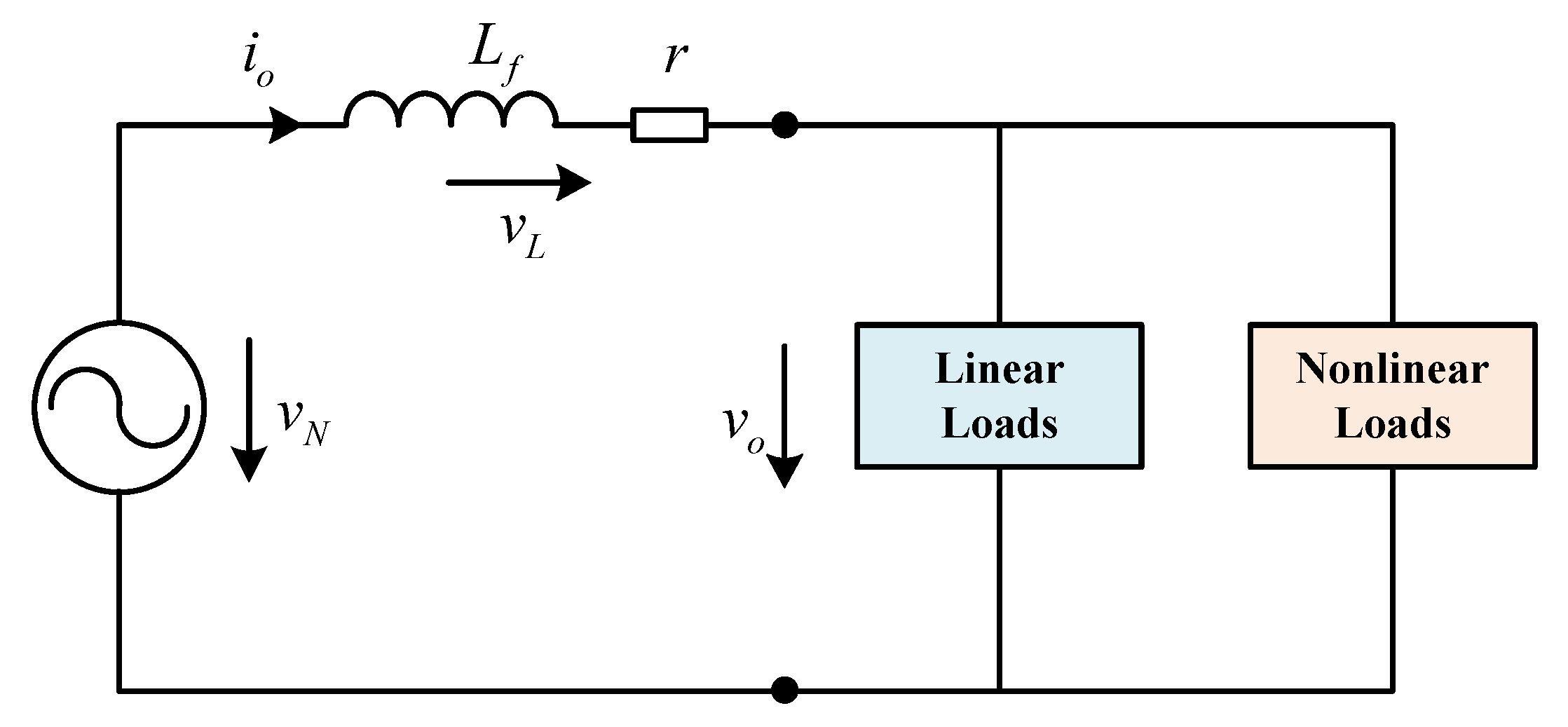
Various researches focus on the harmonic problem of the microgrid. There are two main sources of harmonics in microgrids: power electronic devices and nonlinear loads. Power electronic devices have been widely used in many places, such as inverters, rectifiers, static compensators, etc. The switching of transistors generates high frequency harmonics, which can be suppressed by LC or LCL filter. However, the harmonics generated by nonlinear loads are difficult to be eliminated only by the design of the filter circuit. In an isolated island microgrid, the main reason for generating output voltage harmonics is that nonlinear loads is connected to the inverter terminal to make the output current distorted. When these distorted current flow through the linear electrical components, the corresponding harmonic voltage drop is generated, which eventually leads to the distortion of the inverter output voltage waveform. In order to reduce harmonics and improve system efficiency, harmonic compensation strategies have been extensively studied.
The existing harmonic control researches can be mainly divided into two categories: one is to use the additional compensation devices; the other is to use the harmonic current detection and control algorithm for feedforward compensation without additional compensation devices. Active power filter (APF) is a mature harmonic compensation device, it injects harmonic compensation current with equal magnitude and opposite phase into harmonic source [7,8,9]. Authors in [10] use the least mean squares (LMS, NLMS) and recursive least squares (RLS) algorithms for shunt APF to reduce the total harmonic distortion (THD). But this algorithm has a large computational burden. In [11], a composite control method based on the combination of proportional integral (PI) control and fast repetitive control (FRC) is proposed, which can stabilize the output compensation current in 1/6 grid cycle. However, APF as an additional compensation device in the system, the loss and cost of the device are increased [12,13,14].
Hence, a feedforward compensation strategy based on current detection and control algorithms without additional compensation equipments is considered. A closed loop control of the RMS value of each of the voltage harmonics using PI controller proposed in [15]. The method can suppress each harmonic independently, but it needs to detect the amplitude and phase of each harmonic, and the compensation effect depends on the accuracy of the detection method. Authors in [16] transforms the output voltage of the inverter to the d q synchronous reference frame through the Park transform, and then uses the PI controller to track the reference values of fundamental voltage and harmonics. This method can effectively suppress certain subharmonics, but it needs to design the controller at each compensated harmonics, which makes the control structure complex and parameter tuning difficult. The use of virtual harmonic impedances has also been proposed to harmonic compensation in existing literature [17,18,19]. Authors in [20] proposes a control strategy employs negative virtual harmonic impedance to compensate for effect of line impedance on harmonic power delivery. Authors in [21] propose a composite control strategy of PI and virtual harmonic impedance, and considers the time delay of system. Authors in [22] replaces the PI controller of the fundamental voltage in [21] with the PR controller, which improves the tracking accuracy of the feedback loop. However, the effects of the output inductance value fluctuation on the virtual harmonic impedance compensation effect are not solved in [20,21,22]. Authors in [23] propose adaptive virtual harmonic impedance based on the required voltage quality at the load bus, which solved the uncertainties of virtual harmonic impedances to some extent. But it requires additional calculations for virtual harmonic impedances.
The virtual harmonic impedance can compensate the specific harmonic effectively and simply, but the compensation effect of virtual harmonic impedance is very sensitive to the fluctuation of filter inductance. In order to solve this problem, a composite control strategy combining disturbance rejection control with the virtual harmonic impedance can be considered. At present, common disturbance rejection control strategies include active disturbance rejection control (ADRC), disturbance-observer-based control (DOBC), composite hierarchical antidisturbance control (CHADC) and disturbance accommodation control (DAC), etc. [24]. Unlike many existing control methods, the ADRC does not require the accurate mathematical model of the plant. Therefore, ADRC has been paid more and more attention for its excellent engineering application and disturbance rejection performance, and has been applied in many industries [25,26,27,28]. Authors in [29] proposes a robust active damping method based on the LADRC, to solve the control problem of LCL-filtered grid-connected Inverter in the case of disturbance and parameter uncertainty. A linear auto-disturbance rejection control method based on LCL type grid-connected inverter was proposed in [30], which realized high rejection performance against external interference, internal decoupling and parameter variation.
On the basis of the existing research, Section 2 of this paper firstly models and simplifies the inverter in the d q synchronous reference frame, and then Section 3.2 designs the LADRC controller structure through the relative order of the model and gives the parameter tuning method. In Section 3.1, the virtual harmonic impedance is designed for the high harmonic components of output voltage and feedforward to the fundamental voltage control loop. In Section 4, the stability analysis of LADRC controller and the validity analysis of virtual harmonic impedance are given in the frequency domain. Finally, the good performances of the proposed strategy are shown in Section 5.

2. System Configuration

2.1. Modeling in the d q Synchronous Reference Frame

The LC type three-phase three-leg inverter with proposed control strategy is shown in Figure 1. The LC filter consists of capacitor C f , inductor L f and parasitic resistor r. Although LC filters can reduce switching harmonic, it also produces the output current distortion when feeding nonlinear loads. When these harmonic current flow through the filter inductance and the feeder impedance, it will cause a voltage drop and a output voltage distortion.
According to kirchhoff voltage law and current law, the system model in the a b c reference frame can be written as:
L f d i L k d t = v k N v o k i L k r , C f d v o k d t = i L k i o k .
where k = a , b , c .
Next, the system model in a b c reference frame can be transfromed into d q synchronous reference frame by Park transformation. The system (1) can be expressed as:
L f d i L d d t = v d N v o d i L d r + ω L f i L q , L f d i L q d t = v q N v o q i L q r ω L f i L d , C f d v o d d t = i L d i o d + ω C f v o q , C f d v o q d t = i L q i o q ω C f v o d .
On the d-axis, v d N is the output of inverter before LC filter, v o d is the voltage of loads, i L d is the inductance current and i o d is the current of loads. And v q N , v o q , i L q , i o q have the same definition on the q-axis.
Letting i L d q = i L d + j i L q , v d q N = v d N + j v q N , i o d q = i o d + j i o q , v o d q = v o d + j v o q , form (2) can be rewritten as:
L f d i L d q d t = v d q N v o d q i L d q r j ω L f i L d q , C f d v o d q d t = i L d q i o d q j ω C f v o d q .
From system ( 2 ) , it can be seen that there are strong couplings between d-axis and q-axis. Any disturbance of one axis will affect the other axis by the coupling term, thus affecting the dynamic performance of the system. Therefore, control methods with decoupling functions are required in the d q synchronous reference frame, such as LADRC.

2.2. Model Simplification

The effect of filter capacitor can be disregarded in low frequency systems, hence the main response of the LC filter can be represented by an inductance L f , the simplified circuit is shown in Figure 2. Where v N is the voltage generated by the inverter and v L is the voltage drop of filter inductance and parasitic resistance. i o is the inverter output current, in which low-order harmonic components lead to the distortion of output voltage v o . When the nonlinear loads are far away from the inverter, this distortion will be more serious due to the combined effect of line impedances and filter inductances.
According to the equivalent circuit, v o can be described as:
v o ( t ) = v N ( t ) v L ( t ) = v N ( t ) v L 1 ( t ) n = 2 h v L n ( t ) .
In Equation (4), v L 1 and v L n are the fundamental component and harmonic components of v L and n refers to the harnmonic order. The main implementation of virtual harmonic impedance loops is to design virtual harmonic impedance value equal to the v L n at each frequency to be compensated. Hence, the compensation effect of virtual harmonic impedance loops is very sensitive to inductance value. In order to avoid this problem, a compensation strategy based on LADRC is proposed in this paper. In this strategy, inductance fluctuations are regarded as an unmodelled dynamic, which is estimated by extended state observer (ESO) and then be compensated. In this way, the sensitivity of virtual harmonic impedances to inductance values is reduced. In conclusion, compared with the traditional harmonic compensation strategies, the proposed method has two advantages: decoupling and disturbance rejection.

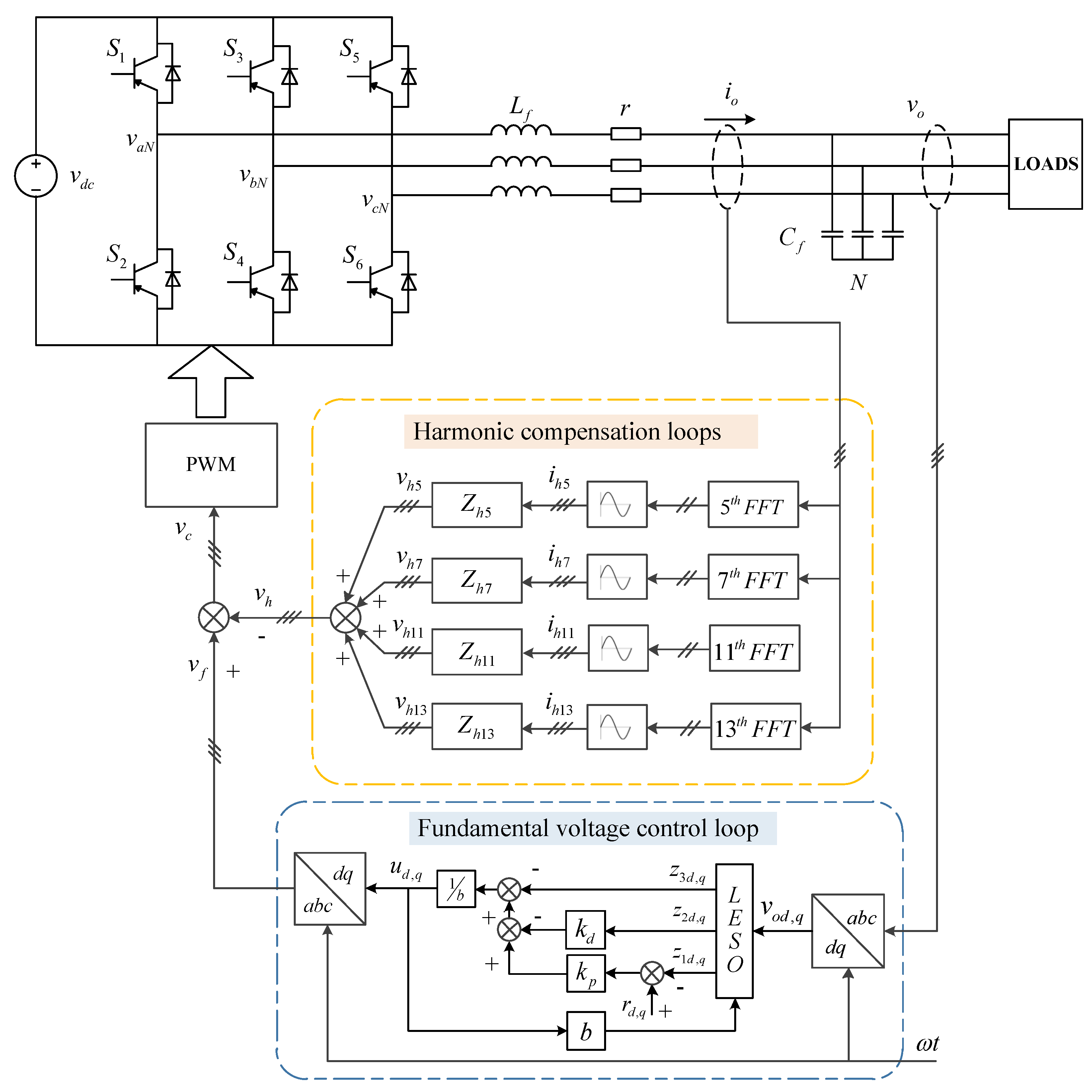
3. Proposed Control Method

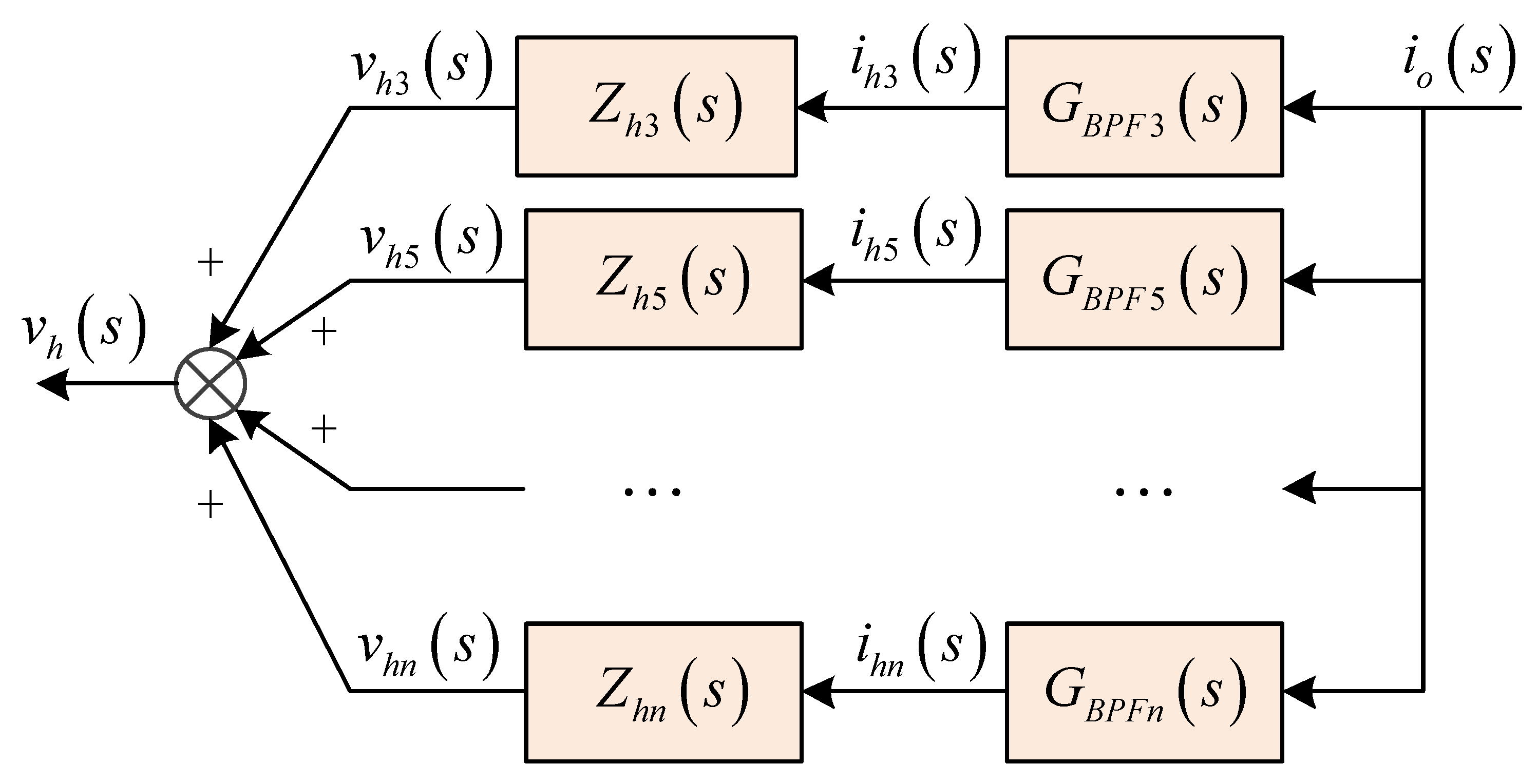
Figure 1 shows the diagram of proposed control, it consists of a fundamental voltage control loop and some specific frequency harmonic compensation loops. The fundamental voltage control loop adopts the LADRC controller in the d q synchronous reference frame, and its output signal is v f . Harmonic compensation loops works by shaping harmonic voltage drops v h with harmonic currents and virtual harmonic impedances. The total output signal of controller is given as follows:
v c = v f v h .

3.1. Virtual Harmonic Impedance Dsign

In harmonic compensation loops, the nth harmonic component from the output current can be detected by Fourier transform. And then the nth harmonic voltage drop is obtained by multiplying the nth harmonic current by the nth virtual harmonic impedance:
v h n = i h n Z h n ,
where i h n is the nth harmonic current and Z h n is the nth virtual harmonic impedance to be designed. The harmonic voltage drop can be added to fundamental voltage control loop inversely. In this way, usually harmonics less than 50th can be compensated without additional compensation inverters.
In order to compensate the voltage drop across the output inductance of the inverter, the v h n should have the same amplitude and opposite phase to v L n :
v h n = v L n = i h n Z L n ,
where Z L n is the output inductance of nth harmonic. It consists of a filter inductor L f and a parasitic resistance r:
Z L n = r + j ω n L f ,
where ω n is the angular frequency of nth harmonic componet.
There are many models of virtual harmonic impedance, such as a resistance, a series RL, a parallel RC, a series RC, etc. In this paper, the virtual harmonic impedance will be modeled as a series RL. This model was chosen because of its simple structure and same form as the output inductance, which simplifies the design process. According to formula (8), the transfer function of a series RL is:
Z h n = R h n + j ω n L h n ,
where R h n = r , L h n = L f , ω n = 2 n π f 1 , f 1 is the fundamental frequency. The amplitude and phase of virtual harmonic impedance denotes as K and θ :
K = | Z h n ( s ) | = R h n 2 + ( ω n L h n ) 2 ,
θ = a r c t a n ( ω n L h n R h n ) .
Hence, the calculation process of the virtual harmonic voltage drop can be equivalent to using a virtual harmonic impedance to perform a K gain and θ phase shift on the harmonic current.

3.2. LADRC Controller Design

This paper proposes the application of LADRC in the fundamental voltage control loop to ensure good tracking of the output voltage reference and robust stability with respect to parametric variations and disturbance. Compared with the PI controller, the proposed strategy has two advantages. One is that it can decouple the model (3) and achieve better transient performance when the load changes. The other is to reject the internal parameter variation and disturbance of the physical system so as to weaken the sensitivity of virtual harmonic impedance effectiveness to output inductance fluctuation.
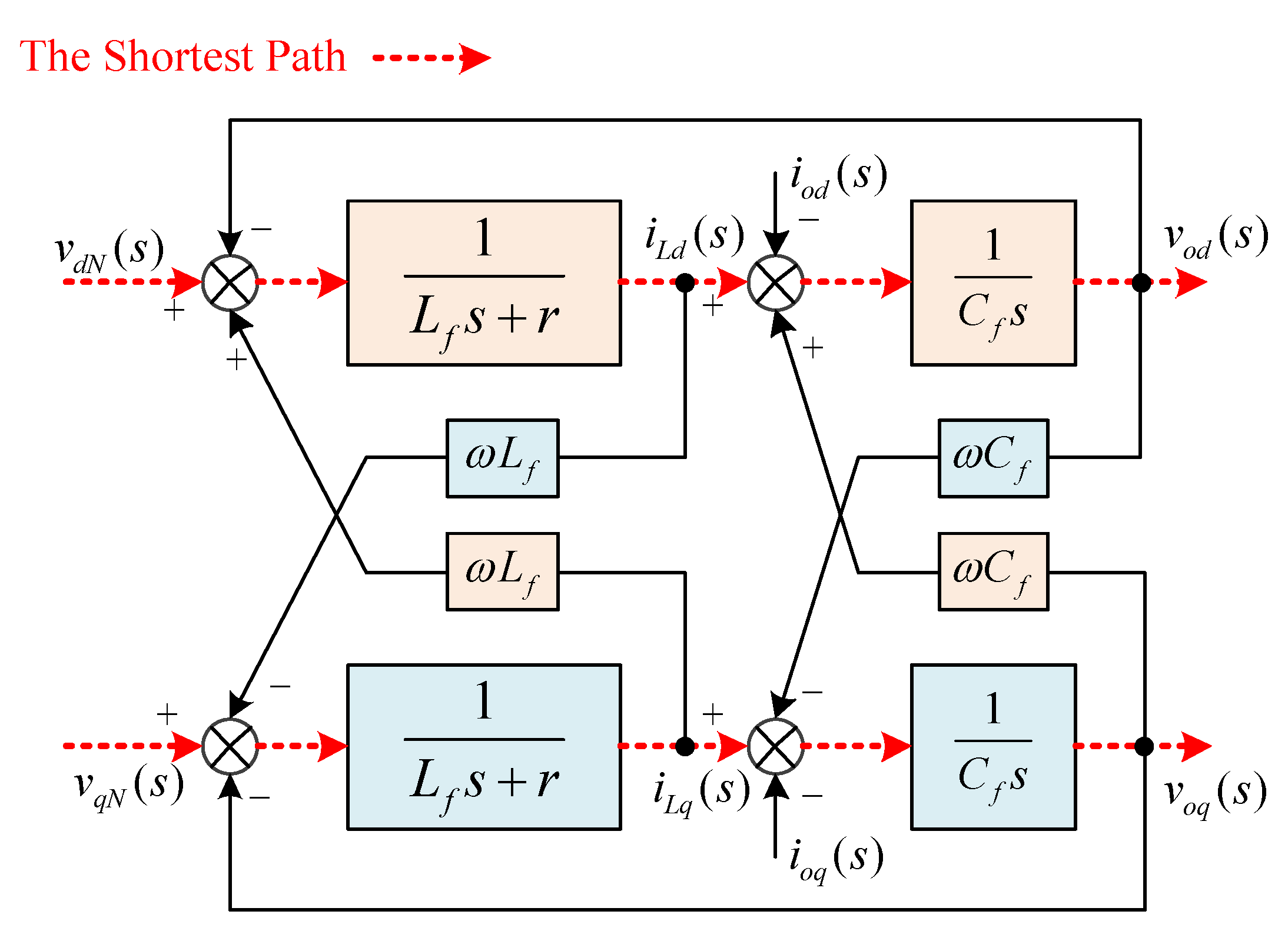
The first step of designing LADRC controller is to determine the relative order of the system. This section uses the shortest path method to obtain the relative order of the system, that is, to find a shortest path from the input to the output through the minimum number of integrators.
According to the system (3), the diagram of LC type inverter in s domain can be drawn, as shown in Figure 3. On d-axis, the input of this system is v d N , the output is v o d , and the shortest path is shown in the red dotted line. There are two integrators on this path, so the the d-axis system is a two-order model. Similarly, the system on the q-axis is also a two-order model.
The system (3) can be written as a second-order plant in the time domain:
v ¨ o d = b v d N + f d , v ¨ o q = b v q N + f q ,
where b = 1 L f C f , it is the input gain of two integrators; f d and f q are the contributions to the output of something other than the input on the shortest path, they be called as total disturbance. The total disturbance includes external disturbances and internal disturbances, such as device parameter fluctuation, load changes, unmodelled dynamics, etc.
In order to simplify ADRC structure, Zhiqiang Gao uses linear gain instead of nonlinear gain, namely LADRC. In this way, the number of parameters is reduced, greatly simplifying the tuning process and providing convenience for engineering applications.
For system (12), a two-order LADRC controller can be designed in Figure 1. LADRC consists of the linear extended state observer (LESO) and the linear state error feedback law (LSEF). LESO is responsible for accurately estimate the total disturbance. The LSEF is responsible for realization of the desired signal by using a feedback controller, such as linear PD. Hence, the effect of LADRC largely depends on the estimation accuracy of the total disturbance.
The controller form of d-axis and q-axis is the same, so plant (12) can be rewritten as a universal two-order state space model:
x ˙ 1 ( t ) = x 2 ( t ) , x ˙ 2 ( t ) = b u ( t ) + f ( t ) , y ( t ) = x 1 ( t ) ,
where y ( t ) represents the output voltage v o d q , it is defined as the first state x 1 ( t ) as usual; the second state x 2 ( t ) is derivative of x 1 ( t ) , which is v ˙ o d q ; f ( t ) represents the total disturbance, which including the variations of the output inductance.
Letting a extended state x 3 ( t ) = f d q ( t ) , the extended state system can be obtained:
x ˙ 1 ( t ) = x 2 ( t ) , x ˙ 2 ( t ) = x 3 ( t ) + b u ( t ) , x ˙ 3 ( t ) = f ˙ ( t ) , y ( t ) = x 1 ( t ) .
Hence, the LESO can be written as:
e ( t ) = z 1 ( t ) x 1 ( t ) , z ˙ 1 ( t ) = z 2 ( t ) β 1 e ( t ) , z ˙ 2 ( t ) = z 3 ( t ) β 2 e ( t ) + b u ( t ) , z ˙ 3 ( t ) = β 3 e ( t ) ,
where z i ( t ) is the estimated value of x i ( t ) , β i is the observer gain ( i = 1 , 2 , 3 ) . With appropriate selection of β i , the z i ( t ) , will track x i ( t ) . The transfer function of the three-order ESO is given by
G e s o 1 ( s ) = z 1 ( s ) y ( s ) = β 1 s 2 + β 2 s + β 3 s 3 + β 1 s 2 + β 2 s + β 3 , G e s o 2 ( s ) = z 2 ( s ) y ( s ) = β 2 s 2 + β 3 s s 3 + β 1 s 2 + β 2 s + β 3 , G e s o 3 ( s ) = z 3 ( s ) y ( s ) = β 3 s 2 s 3 + β 1 s 2 + β 2 s + β 3 .
The observer gains can be selected by bandwidth-parameterization method [31], such that all the observer eigenvalues are placed at ω o , then β 1 = 3 ω o , β 2 = 3 ω o 2 , β 3 = ω o 3 . Denote ω o as the observer bandwidth.
Base on the estimation of the state of the system, the linear PD controller is used to track the reference value r ( t ) and the estimation of the total disturbance is subtracted from PD control law to compensate the disturbance. Hence, in the s domain the transfer function of the LSEF can be expressed as:
u ( s ) = u 0 ( s ) z 3 ( s ) b ,
u 0 ( s ) = k p [ r ( s ) z 1 ( s ) ] k d z 2 ( s ) .
The parameters k p and k d can also be selected by bandwidth-parameterization method, generally k p = 2 ω c , k d = ω c 2 . Denote ω c as the observer bandwidth.
Substitute (15) into controlled plant results in:
x ˙ 2 = u 0 z 3 + f .
Thus, the total disturbance will be eliminated once z 3 is approximately equal to f.
To obtain the transfer function of the LADRC controller, combine (16)–(18):
u ( s ) = G u r ( s ) r ( s ) G u y ( s ) y ( s ) ,
where
G u r ( s ) = k p b ,
G u y ( s ) = k p G e s o 1 ( s ) + k d G e s o 2 ( s ) + G e s o 3 ( s ) b
And then, the stability of LADRC controller and virtual harmonic impedance will be proved in the Section 4.

4. Stability and Disturbance Rejection Analysis

In this section, the stability of the fundamental voltage control loop and the harmonic compensation loop is proved. Furthermore, a disturbance rejection analysis regarding to variations of the output LC filter parameters is shown.
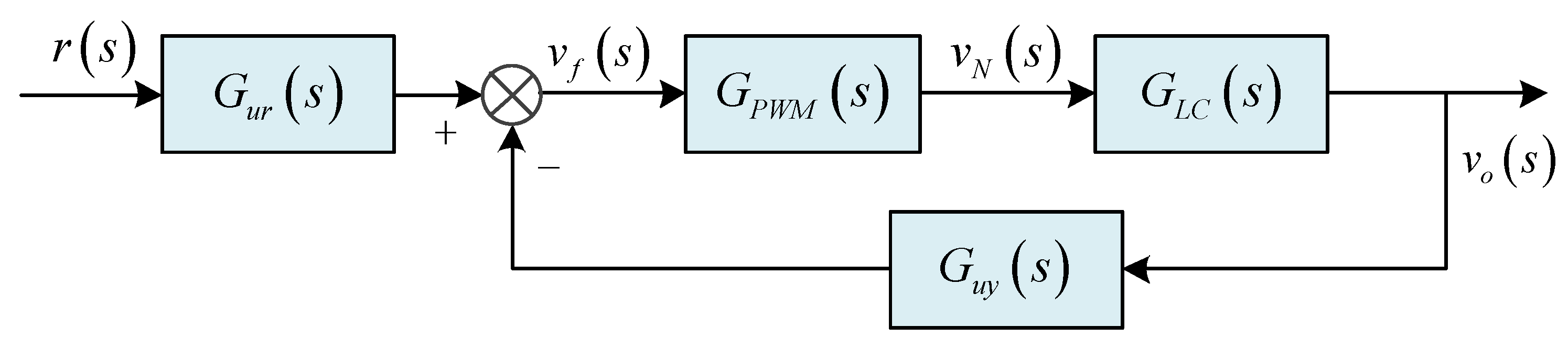
The block diagram of the fundamental voltage control loop transfer function under no load conditions is shown in Figure 4. Where v o ( s ) is the voltage of loads, which is y ( s ) of transfer function (20). r ( s ) is the reference voltage and v N ( s ) is the voltage generated by the inverter. The output signal of LADRC controller is denoted as v f ( s ) (d-axis has the same form as the q-axis), which is u ( s ) of transfer function (20). G L C ( S ) is the LC filter transfer function, G P W M ( s ) is the relationship between v N ( s ) and v f ( s ) . G u r ( s ) and G u y ( s ) are given by transfer function (21) and (22) respectively.
Due to the no load conditions, the i o k in the model (1) is equal to zero, then the transfer function between v o ( s ) and v N ( s ) can be written as:
G L C ( s ) = v o ( s ) v N ( s ) = 1 L f C f s 2 + r C f s + 1 .
In this paper, according to the state space averaging method, the switching function of the IGBT is linearized, and the pulse width modulation method is adopted. The relationship between the modulation signals v f ( s ) and the inverter generated voltage v N ( s ) can be regarded as an one-order inertia unit:
G P W M ( s ) = v N ( s ) v f ( s ) v d c 2 v t r i ( T s + 1 ) ,
where v t r i is the amplitude of the triangle wave, v d c is the DC voltage. By combining (21)–(24), the transfer function of the fundamental voltage control loop can be expressed as:
G s y s 1 ( s ) = v o ( s ) r ( s ) = G r ( s ) 1 + G y ( s ) ,
where
G r ( s ) = G u r ( s ) G P W M ( s ) G L C ( s ) ,
G y ( s ) = G u y ( s ) G P W M ( s ) G L C ( s ) .
Letting L f = 2.5 mH, C f = 4.7 μ F, r = 1.5 Ω , b = 1 L f C f , k p = ω c 2 , k d = 2 ω c , ω c = 200 , β 1 = 3 ω o , β 2 = 3 ω o 2 , β 3 = ω o 3 , ω o = 5 ω c , v d c = 30 V, v t r i = 12.5 V, T = 
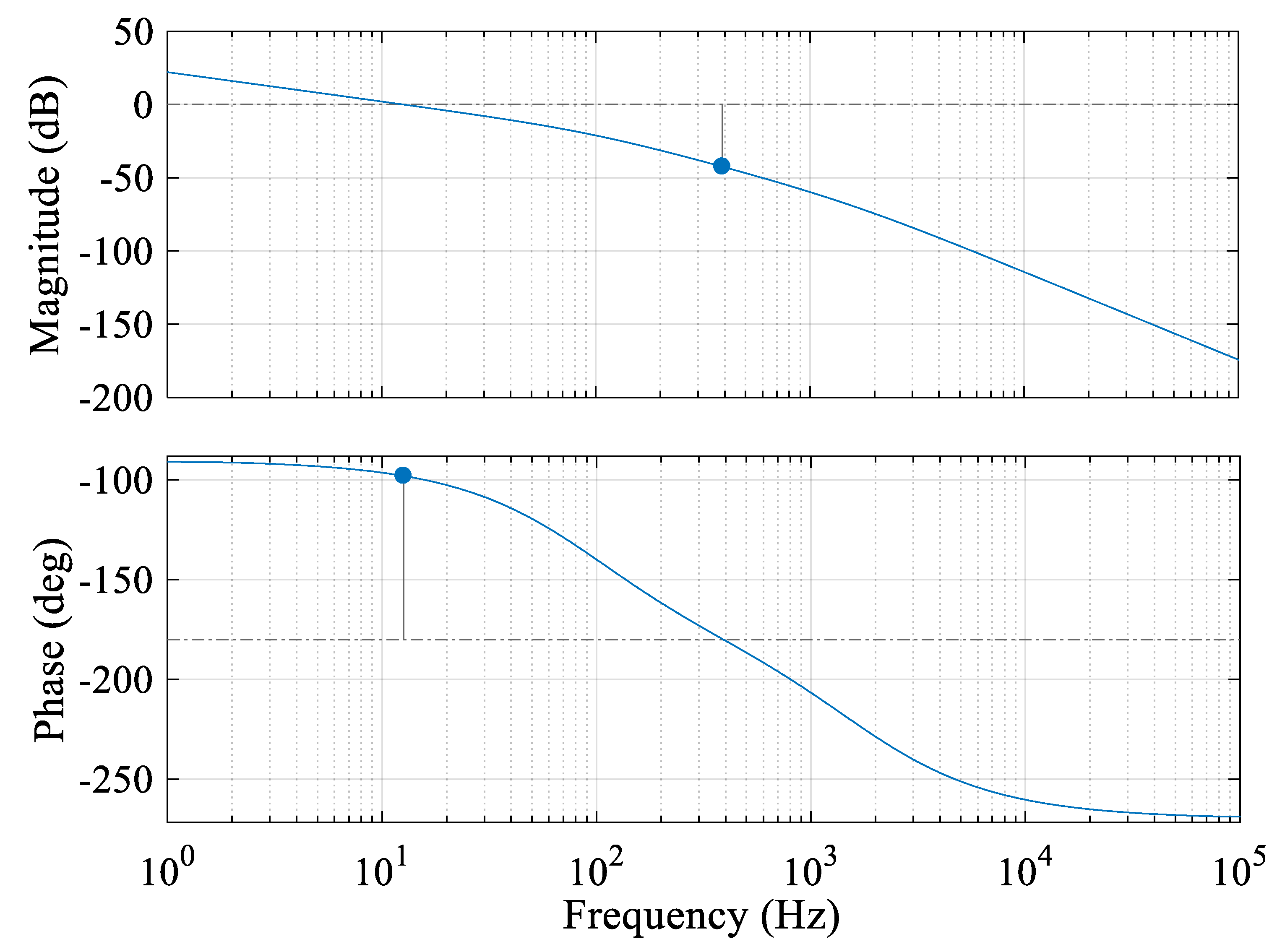
0.0001 s. The frequency response of G s y s 1 ( s ) can be obtained, as shown in Figure 5.
As can be seen from the Bode plot, the phase margin of G s y s 1 ( s ) is 82 deg at 12.6 Hz and the amplitude margin is 42.4 dB at 390 Hz. Moreover, systems with phase margins greater than 45 deg in engineering experience have good dynamic performance. Therefore, the stability and dynamics of the fundamental voltage control loop are excellent.
The proposed strategy adds a virtual harmonic impedance branch to the fundamental voltage control loop, similar to the feedforward-feedback composite control method. Therefore, based on the stability analysis of the feedback loop, the frequency response of the feedforward loops needs to be analyzed.
The block diagram of the transfer function of multiple virtual harmonic impedances in parallel is shown in Figure 6, where v h is the total harmonic voltage drop shaped by harmonic currents and virtual harmonic impedances, Z h n ( s ) is the nth virtual harmonic impedance.
The premise of harmonic compensation using virtual harmonic impedance is the extraction of harmonic components in the current signal. To simplify the analysis, the extraction process is approximated as a bandpass filter G B P F n ( s ) designed at the harmonic frequencies ω n that need to be compensated:
G B P F n ( s ) = k ω n s Q s 2 + ω n s + Q ω n 2 ,
where ω n is the center frequency of the extracted harmonic components, k is the gain of center frequency, Q is the quality factor. The transfer function of the virtual harmonic impedance is G s y s 2 , which can characterize the relationship between i o ( s ) and v h ( s ) . By combing (9) and (28), the transfer function of this loop can be obtained:
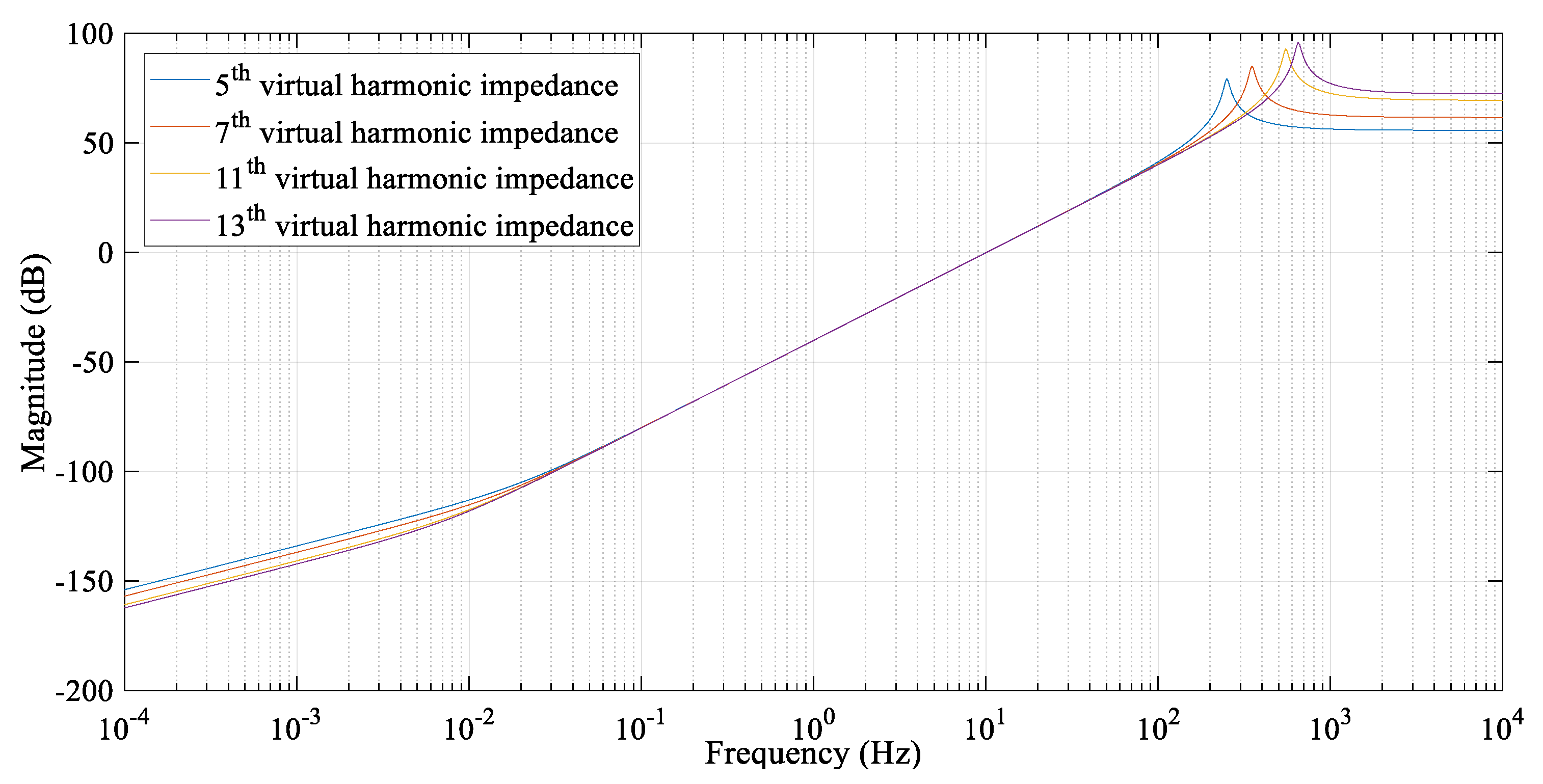
G s y s 2 ( s ) = i = 3 n Z h i ( s ) G B P F i ( s ) .
Due to the 6 k ± 1 times harmonics are the main components of harmonic current under the nonlinear loads, and the harmonic content is attenuated with the increase of harmonic frequency, this paper selects the 5th, 7th, 11th and 13th harmonics for compensation.
Letting k = 1.5 , Q = 15 , R h 5 = R h 7 = R h 11 = R h 13 = 1.5 Ω , L h 5 = 3.927 H, L h 7 = 5.498 H, L h 11 = 8.639 H, L h 13 = 10.210 H. The frequency response of each individual virtual harmonic impedance is shown in Figure 7. It can be seen that the designed virtual harmonic impedance (including the extraction units) has a high positive gain at 250 Hz, 350 Hz, 550 Hz, and 650 Hz, respectively.
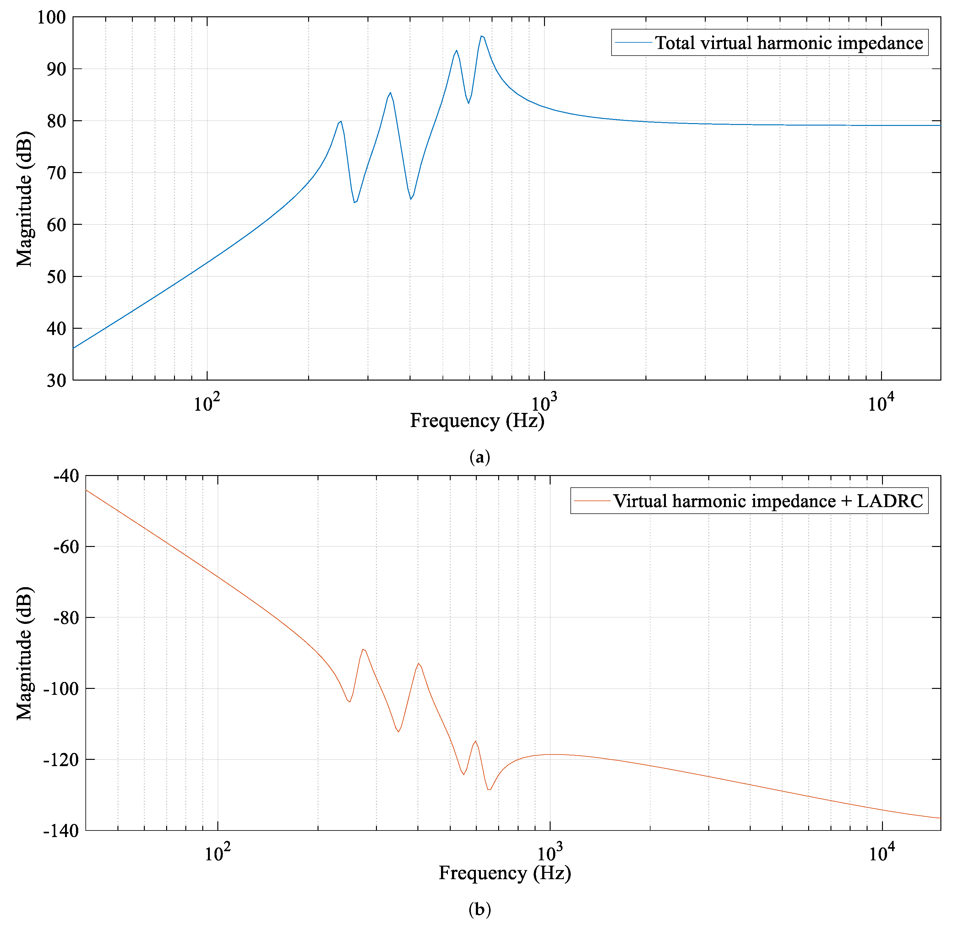
Frequency responses of (29) ( i = 5 , 7 , 11 , 13 ) and proposed method are shown in Figure 8. It can be seen from Figure 8b that the whole system exhibits a larger negative gain at the selected frequency, which reduces the equivalent output impedance of the system, so the harmonic voltage drop generated by the harmonic current is reduced. This conclusion proves the validity of the feedforward loop.
Furthermore, as virtual harmonic impedance effectiveness depends on the real inductance value L f , in this section a sensitivity analysis regarding to variations of the output LC filter parameters is shown in Figure 9. It can be seen that compared with PI, the use of LADRC makes the output inductance fluctuation have less influence on the harmonic compensation effect. Authors in [21] indicates that the value of parasitic resistance has a weak influence on the virtual harmonic impedance, so the influence of parasitic resistance in this paper is not studied.

5. Simulation and Experimental Results

In order to verify the performances of the proposed strategy, simulations and experiments are designed in this section. A LC type three-phase three-leg inverter of Figure 1 is used, and a resistive linear load and a non-linear load are respectively connected to the output terminals. The nonlinear load consists of a three-phase full-bridge rectifier and a series resistive and inductive load. In order to ensure the reasonableness of the comparison, when the virtual harmonic impedance parameters of the design are unchanged, the PI and LADRC algorithms are used in the fundamental voltage control loop respectively.

5.1. Simulation Results

The circuit parameters and controller parameters in the simulation are shown in Table 1 and Table 2. In order to prove the performance of the proposed strategy, two comparative simulations were designed, as shown in Table 3, and the results are shown in Figure 10. It can be seen that the transient response speed of LADRC is faster than PI. The transition time with PI is 0.07 s (3.5 periods), while the transition time with LADRC is 0.03 s (1.5 periods), and the rapidity of the system is increased by 57.1%. This is mainly because there are two coupling terms in the dual-loop PI control strategy in the d q synchronous reference frame. When the system state changes, the d-axis and the q-axis will affect each other. However, the LADRC controller puts coupling terms into the total disturbance to achieve decoupling and improve response speed.
In addition, in the condition of open loop and two strategies, harmonic contents are shown in Table 4. It can be seen that when open loop control, THD (only the first 20 harmonics are counted) is 9.35 % , and the 5th, 7th, 11th, and 13th harmonic contents are 5.00%, 3.50%, 2.90%, and 2.95%, respectively. With the proposed strategy, the THD is reduced to 2.30%, the harmonic compensation is up to 75.4%, and each compensated component is reduced to less than 1% (the 5th, 7th, 11th, and 13th harmonic contents is reduced to 0.87%, 0.60%, 0.85%, and 0.74%, respectively). If PI control is used in the fundamental voltage control loop, the THD drops to 2.50%, and the compensated harmonic components are also significantly reduced. It can be confirmed that the virtual harmonic impedance designed in this paper can effectively compensate for harmonics at selected frequencies.
Although PI and LADRC have almost the same suppression of selected harmonics, it can be seen from Figure 10a that when PI is used, there are many high-frequency components in the output voltage. Larger inductance parameters are often used to eliminate this ripple, but the inductance is proportional to its volume, which takes up more space and results in additional power loss and expense.

5.2. Experimental Results

Compared with the controller without disturbance rejection function, the advantage of LADRC is mainly reflected in the fact that the fluctuation of the filter inductance parameter has less influence on the compensation effect of virtual harmonic impedance loops. This feature of LADRC is not significant in the ideal environment for simulation. However, since the actual physical system is a non-ideal system, the fluctuation of the inductance L f cannot be eliminated, so this feature is meaningful in the physical experiment.
In this paper, an experimental platform is built (shown in Figure 11), which includes an LC type three-phase three-leg inverter, a Speedgoat real-time controller, a Faith DC power source, a three-phase linear Load, a nonlinear load, a Hioki power quality analyzer and a four-channel oscilloscope. The Speedgoat real-time controller consists of a real-time target machine, an input module and an output module. The hardware circuit topology and parameter selection of inverter are the same as those in Section 5.1. The circuit parameters and the controller parameters are shown in Table 1 and Table 5, respectively.
Three sets of experiments were designed for comparison in this section, as shown in Table 6.
As shown in Figure 12a, there is a significant distortion of the output voltage waveforms under the open loop control. In addition, due to the non-ideality of the three-phase linear load, there is a slight unbalance in the output voltage. Figure 12c shows the output voltage waveforms under the control of the dual-loop PI at the fundamental voltage control loop. As can be seen from this figure, the harmonics in the output voltage are partially compensated, but there are still significant distortions. Moreover, the three-phase unbalance has not improved. Figure 12e shows the output voltage waveforms under the proposed control strategy. It can be seen that the harmonics of the output voltage are significantly compensated. Moreover, the three-phase unbalance problem has also been improved. The reason for this effect is that LADRC can estimate and compensate for disturbances in the system and unmodelled dynamics (i.e., total disturbance f), thereby improving power quality.
The compensation effect of the three experiments can be measured by the power quality analyzer, as shown in Figure 12b,d,f. It can be seen that although experiment 2 has some compensation on the 5th, 7th, 11th and 13th harmonics, it raises the distortion content near the compensated harmonics, for example, 6th, 8th, and 12th. The main reason is that the inductance value fluctuates during the operation of the physical system, which results in the virtual harmonic impedance compensation effect are not ideal. Since LADRC estimates and compensates for the parameter fluctuation of the filter inductor, the effect of the virtual harmonic impedance is less sensitive to the inductance variation. The proposed strategy shows better harmonic compensation effect. The proposed control strategy reduced THD from 8.36% to 4.37%, and the 5th, 7th, 11th and 13th harmonics decreased from 4.85%, 4.66%, 2.63%, and 2.48% to 0.90%, 0.94%, 0.85%, and 0.81%, respectively.

6. Discussion

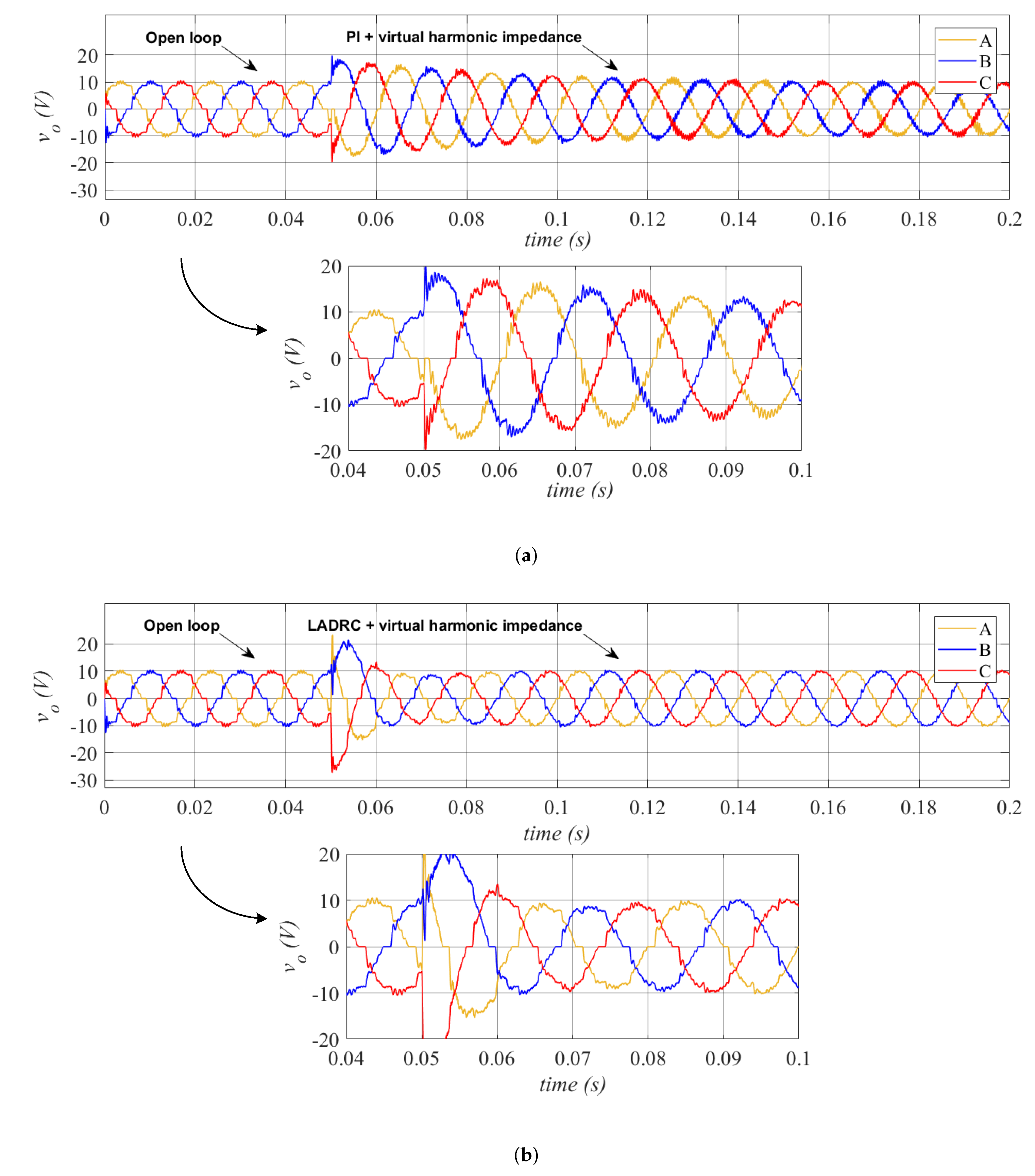
This paper proposes a harmonic compensation strategy based on LADRC and virtual harmonic impedance for LC type three-phase three-leg inverter.
Firstly, the proposed strategy considers the fluctuation of the filter inductance as the unmodelled dynamics of the system and reduces the sensitivity of the virtual harmonic impedance to the filter inductance through the observation and compensation of LADRC, which is shown in Figure 9. Therefore, when the filter inductance fluctuates in actual engineering, the proposed control strategy has better harmonic compensation effect. In 
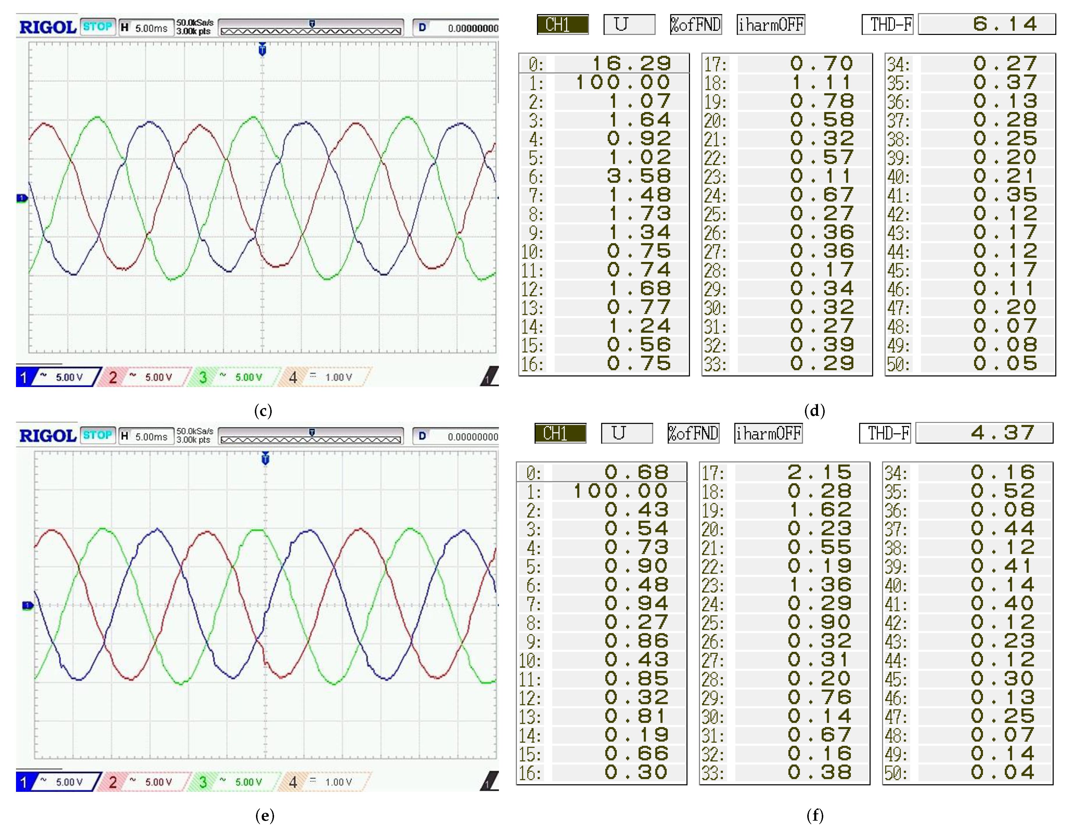
Section 5.2 demonstrates this advantage through physical experiments.
Secondly, the proposed method does not require additional compensation devices, which reduces power loss and cost, and has higher economic and application value. As the harmonic compensation loops increases, the computational complexity of the method will increase, but this method is a flexible and effective strategy for specific compensation of harmonic components with higher content in the output voltage.
Finally, the proposed strategy can decouple the system model and eliminate the interaction between the d-axis and the q-axis to improve the transient recovery speed. Decoupling the model reduces the number of sensors in physical experiments, from 9 sensors (with PI controllers) to 6 sensors (with LADRC controllers).
In summary, the proposed method has better control performance and engineering applicability, which is verified by simulations and experiments. However, as the number of harmonics that need to be compensated increases, the amount of calculation also increases. In the next studies, a harmonic full compensation strategy with less computational complexity can be studied.
References

Author Contributions

Methodology, H.L. and Y.Q.; validation, H.L., Y.Q. and S.L.; writing—original draft preparation, H.L. and Y.Q.; writing—review and editing, H.L., Y.Q. and S.L.; supervision, J.L.; project administration, H.L. and J.L.; funding acquisition, H.L. and J.L.

Funding

This research was supported by Shanghai International Science and Technology Cooperation Program (No. 15220710500), Shanghai Science and Technology Commission Key Program (No. 18DZ1203200) and Shanghai Science and Technology Commission Local College Capacity Building Program (No. 15160500800).

Conflicts of Interest

The authors declare no conflict of interest.

References

  1. Liu, J.; Rahman, M.S.; Lu, J.; Hossain, M.J. Performance investigation of hybrid AC/DC microgrids during mode transitions. In Proceedings of the 2016 Australasian Universities Power Engineering Conference (AUPEC), Brisbane, Australia, 25–28 September 2016. [Google Scholar]
  2. Guerrero, J.M.; Loh, P.C.; Lee, T.L.; Chandorkar, M. Advanced Control Architectures for Intelligent Microgrids—Part II: Power Quality, Energy Storage, and AC/DC Microgrids. IEEE Trans. Ind. Electron. 2012, 60, 1263–1270. [Google Scholar] [CrossRef]
  3. Khadkikar, V. Enhancing Electric Power Quality Using UPQC: A Comprehensive Overview. IEEE Trans. Power Electron. 2012, 27, 2284–2297. [Google Scholar] [CrossRef]
  4. Wagner, V.E.; Balda, J.C.; Griffith, D.C.; Mceachern, A.; Barnes, T.M.; Hartmann, D.P.; Phileggi, D.J.; Emannuel, A.E.; Horton, W.F.; Reid, W.E. Effects of harmonics on equipment. IEEE Trans. Power Deliv. 1993, 8, 672–680. [Google Scholar] [CrossRef]
  5. Safargholi, F.; Malekian, K.; Schufft, W.; Safargholi, F.; Malekian, K.; Schufft, W. On the Dominant Harmonic Source Identification-Part I: Review of Methods. IEEE Trans. Power Deliv. 2017, 33, 1268–1277. [Google Scholar] [CrossRef]
  6. Shuai, Z.; Luo, A.; Shen, J.; Wang, X. Double Closed-Loop Control Method for Injection-Type Hybrid Active Power Filter. IEEE Trans. Power Electron. 2011, 26, 2393–2403. [Google Scholar] [CrossRef]
  7. Singh, B.; Al-Haddad, K.; Chandra, A. Review of active filters for power quality improvement. IEEE Trans. Ind. Electron. 2008, 46, 960–971. [Google Scholar] [CrossRef]
  8. Briz, F.; Diaz-Reigosa, D.; Degner, M.W.; Garcia, P.; Guerrero, J.M. Dynamic behavior of current controllers for selective harmonic compensation in three-phase active power filters. IEEE Trans. Ind. Appl. 2013, 49, 1411–1420. [Google Scholar] [CrossRef]
  9. Taghizadeh, S.; Hossain, M.J.; Lu, J.; Karimi-Ghartemani, M. An Enhanced DC-Bus Voltage-Control Loop for Single-Phase Grid-Connected DC/AC Converters. IEEE Trans. Power Electron. 2019, 34, 5819–5829. [Google Scholar] [CrossRef]
  10. Martinek, R.; Rzidky, J.; Jaros, R.; Bilik, P.; Ladrova, M. Least Mean Squares and Recursive Least Squares Algorithms for Total Harmonic Distortion Reduction Using Shunt Active Power Filter Control. Energies 2019, 12, 1545. [Google Scholar] [CrossRef]
  11. Xie, N.; Xu, Q.; Zeng, J.; Liu, X.; Zhang, W.; Zhang, C. Noval hybrid control method for APF based on PI and FRC. J. Eng. 2019, 2019, 3002–3006. [Google Scholar] [CrossRef]
  12. Jiang, F.; Li, Y.; Tu, C.; Guo, Q.; Li, H. A review of series voltage source converter with fault current limiting function. Chin. J. Electr. Eng. 2018, 4, 36–44. [Google Scholar]
  13. Chen, D.; Xie, S. Review of the control strategies applied to active power filters. In Proceedings of the IEEE International Conference on Electric Utility Deregulation, Hong Kong, China, 5–8 April 2004. [Google Scholar]
  14. Wang, Y.W.; Wong, M.C.; Lam, C.S. Historical review of parallel hybrid active power filter for power quality improvement. In Proceedings of the TENCON 2015—2015 IEEE Region 10 Conference, Macao, China, 1–4 November 2016. [Google Scholar]
  15. Patel, H.; Agarwal, V. Control of a Stand-Alone Inverter-Based Distributed Generation Source for Voltage Regulation and Harmonic Compensation. IEEE Trans. Power Deliv. 2008, 23, 1113–1120. [Google Scholar] [CrossRef]
  16. De, D.; Ramanarayanan, V. A Proportional & Multiresonant Controller for Three-Phase Four-Wire High-Frequency Link Inverter. IEEE Trans. Power Electron. 2010, 25, 899–906. [Google Scholar]
  17. Zhong, Q.C.; Zeng, Y. Control of Inverters Via a Virtual Capacitor to Achieve Capacitive Output Impedance. IEEE Trans. Power Electron. 2014, 29, 5568–5578. [Google Scholar] [CrossRef]
  18. Micallef, A.; Staines, C.S.; Guerrero, J.M.; Vasquez, J.C.; Apap, M. Reactive Power Sharing and Voltage Harmonic Distortion Compensation of Droop Controlled Single Phase Islanded Microgrids. IEEE Trans. Smart Grid 2014, 5, 1149–1158. [Google Scholar] [CrossRef]
  19. De Brabandere, K.; Bolsens, B.; Van den Keybus, J.; Woyte, A.; Driesen, J.; Belmans, R. A Voltage and Frequency Droop Control Method for Parallel Inverters. IEEE Trans. Power Electron. 2007, 22, 1107–1115. [Google Scholar] [CrossRef]
  20. Sreekumar, P.; Khadkikar, V. A New Virtual Harmonic Impedance Scheme for Harmonic Power Sharing in an Islanded Microgrid. IEEE Trans. Power Deliv. 2016, 31, 936–945. [Google Scholar] [CrossRef]
  21. Arricibita, D.; Sanchis, P.; Gonzalez, R.; Marroyo, L. Impedance Emulation for Voltage Harmonic Compensation in PWM Stand-Alone Inverters. IEEE Trans. Energy Convers. 2017, 32, 1335–1344. [Google Scholar] [CrossRef]
  22. Tu, C.; Yi, Y.; Fan, X.; Zheng, L.; Li, Y. The Output Side Power Quality Control Strategy for Microgrid Main Inverter under Nonlinear Load. Trans. Chin. Electrotech. Soc. 2018, 32, 53–62. [Google Scholar]
  23. Savaghebi, M.; Shafiee, Q.; Vasquez, J.C.; Guerrero, J.M. Adaptive virtual impedance scheme for selective compensation of voltage unbalance and harmonics in microgrids. In Proceedings of the 2015 IEEE Power & Energy Society General Meeting, Denver, CO, USA, 26–30 July 2015. [Google Scholar]
  24. Chen, W.H.; Yang, J.; Lei, G.; Li, S. Disturbance Observer-Based Control and Related Methods: An Overview. IEEE Trans. Ind. Electron. 2016, 63, 1083–1095. [Google Scholar] [CrossRef]
  25. Han, J. From PID to Active Disturbance Rejection Control. IEEE Trans. Ind. Electron. 2009, 56, 900–906. [Google Scholar] [CrossRef]
  26. Yi, H.; Xue, W.; Yang, X. Active disturbance rejection control: Methodology, theoretical analysis and applications. In Proceedings of the 9th Chinese Control Conference, Beijing, China, 29–31 July 2010. [Google Scholar]
  27. Sun, B.; Gao, Z. A DSP-based active disturbance rejection control design for a 1-kW H-bridge DC-DC power converter. IEEE Trans. Ind. Electron. 2005, 52, 1271–1277. [Google Scholar] [CrossRef]
  28. Zheng, Q.; Dong, L.; Lee, D.H.; Gao, Z. Active Disturbance Rejection Control for MEMS Gyroscopes. IEEE Trans. Control Syst. Technol. 2009, 17, 1432–1438. [Google Scholar] [CrossRef]
  29. Benrabah, A.; Xu, D.; Gao, Z. Active Disturbance Rejection Control of LCL -Filtered Grid-Connected Inverter Using Padé Approximation. IEEE Trans. Ind. Appl. 2018, 54, 6179–6189. [Google Scholar] [CrossRef]
  30. Lu, J.; Savaghebi, M.; Guerrero, J.M.; Vasquez, J.C.; Xie, C. Linear active disturbance rejection control for LCL type grid-connected converter. In Proceedings of the IECON 2016—42nd Annual Conference of the IEEE Industrial Electronics Society, Florence, Italy, 23–26 October 2016. [Google Scholar]
  31. Gao, Z. Scaling and Parameterization Based Controller Tuning. In Proceedings of the American Control Conference, Denver, CO, USA, 4–6 June 2003. [Google Scholar]
Figure 1. A LC type three-phase three-leg inverter with proposed control strategy.
Energies 12 02618 g001
Figure 2. Equivalent circuit of the virtual harmonic impedance loop.
Energies 12 02618 g002
Figure 3. The shortest path of LC inverter model in s domain.
Energies 12 02618 g003
Figure 4. The transfer function of the fundamental voltage control loop.
Energies 12 02618 g004
Figure 5. Bode plot of the transfer function of the fundamental voltage control loop.
Energies 12 02618 g005
Figure 6. The transfer function of the harmonic compensation loop.
Energies 12 02618 g006
Figure 7. Frequency response of virtual harmonic impedance.
Energies 12 02618 g007
Figure 8. (a) Frequency response of total virtual harmonic impedance. (b) Frequency response of proposed method.
Energies 12 02618 g008
Figure 9. The relationship between theoretical compensation degree and parameter variation.
Energies 12 02618 g009
Figure 10. (a) The output voltage with PI and virtual harmonic impedance. (b) The output voltage with LADRC and virtual harmonic impedance.
Energies 12 02618 g010
Figure 11. Experimental platform.
Energies 12 02618 g011
Figure 12. (a) Output voltage waveforms for experiment 1. (b) THD for experiment 1. (c) Output voltage waveforms for experiment 2. (d) THD for experiment 2. (e) Output voltage waveforms for experiment 3. (f) THD for experiment 3.
Energies 12 02618 g012aEnergies 12 02618 g012b
Table 1. Circuit Parameters.
SymbolQuantityValue
f s Switching frequency10 kHz
f 1 Fundamental frequency50 Hz
L f Filter inductance2.5 mH
rParasitic resistance1.5 Ω
C f Filter capacitance4.7 μ F
L n l Inductance of nonlinear load9 mH
R n l Resistance of nonlinear load28 Ω
R l Resistance of linear load73 Ω
Table 2. Controller Parameters in Simulations.
Virtual Harmonic ImpedanceLADRCDual-Loop PI Control
SymbolValueSymbolValueSymbolValueSymbolValueSymbolValue
L h 5 3.927 H R h 5 1.5 Ω ω c 2500 ω o 1.25 × 10 4 k p i n n e r l o o p 1
L h 7 5.498 H R h 7 1.5 Ω k p 6.25 × 10 6 k d 5000 k i i n n e r l o o p 10
L h 11 8.639 H R h 11 1.5 Ω β 1 3.75 × 10 4 β 2 4.69 × 10 8 k p o u t e r l o o p 1.5
L h 13 10.210 H R h 13 1.5 Ω β 3 1.95 × 10 12 b 8.51 × 10 7 k i o u t e r l o o p 10
Table 3. The Design of Simulations.
No.0–0.05 s0.05–0.20 s
Simulation 1Open loopPI + virtual harmonic impedance
Simulation 2Open loopLADRC + virtual harmonic impedance
Table 4. HarmonicContents.
Harmonic Orderwithout CompensationSimulation 1Simulation 2
THD9.35%2.58%2.30%
5th5.00%1.08%0.87%
7th3.50%0.74%0.60%
11th2.90%0.91%0.85%
13th2.95%0.79%0.74%
Table 5. Controller Parameters in Experiments.
Virtual Harmonic ImpedanceLADRCDual-Loop PI Control
SymbolValueSymbolValueSymbolValueSymbolValueSymbolValue
L h 5 3.797 H R h 5 1.257 Ω ω c 400 ω o 2000 k p i n n e r l o o p 3
L h 7 7.878 H R h 7 1.389 Ω k p 1.60 × 10 5 k d 800 k i i n n e r l o o p 5
L h 11 9.880 H R h 11 1.488 Ω β 1 6000 β 2 1.20 × 10 7 k p o u t e r l o o p 0.2
L h 13 13.880 H R h 13 1.769 Ω β 3 8.00 × 10 9 b 8.51 × 10 7 k i o u t e r l o o p 10
Table 6. The Design of Experiments.
No.Fundamental Voltage Control LoopHarmonic Compensation Loops
Experiment 1Open loopOpen loop
Experiment 2Dual-loop PI controlVirtual harmonic impedance
Experiment 3LADRCVirtual harmonic impedance

