Article

Design and Implementation of a Low-Power Low-Cost Digital Current-Sink Electronic Load

1
Department of Electrical Engineering, Yangzhou University, Yangzhou 225000, China
2
Division of Electronics and Informatics, Gunma University, Kiryu 376-8515, Japan
3
State Grid Yangzhou Power Supply Company, Yangzhou 225000, China
*
Author to whom correspondence should be addressed.
Current address: No. 88 University Avenue, Yangzhou 225000, China.
This paper is an extended version of our paper published in the 2013 IEEE Power Electronics and Drive Systems Conference, Kitakyushu, Japan, 22–25 April 2013.
Energies 2019, 12(13), 2611; https://doi.org/10.3390/en12132611
Submission received: 30 April 2019 / Revised: 3 July 2019 / Accepted: 4 July 2019 / Published: 7 July 2019

Abstract

:
Electronic load (e-load) is essential equipment for power converter performance test, where a designated load profile is executed. Electronic load is usually implemented with the analog controller for fast tracking of the load profile reference. In this paper, a low-power low-cost electronic load is proposed. MOSFETs (metal-oxide-semiconductor field-effect transistors) are used as the power consumption devices, which are regulated to the active region as controlled current-sink. In order to achieve fast transient response using the low-cost digital signal controller (DSC) PWM peripherals, the interleaving PWM method is proposed to achieve active current ripple mitigation. To obtain the system open-loop gain for current-sink operation, an offline digital system identification method, followed by model reduction, is proposed by applying Pseudo-Random Binary Sequence (PRBS) excitation. Pole-zero cancelation method is used in the control system design and later implemented in a DSC. The prototype is built and tested, in which meaningful testing scenarios under constant current-sink mode, pulse current sink mode, and double line-frequency current mode are verified. The experimental results indicate that the proposed e-load can sink pre-programmed current profile with well-attenuated ripple for static and dynamic load testing, and is applicable to fully digitalized power testing equipment.

Graphical Abstract

1. Introduction and Objectives

Electronic load (e-load) plays a key role in modern electronic systems, energy systems, and power distribution systems design flow [1,2,3,4]. The e-load can sink power from the Unit Under Test (UUT) following the designated load pattern for power testing purposes [5,6,7]. The electric power generated by the UUT can be either sent back the grid or transferred to a dissipating load. There are two kinds of dissipative e-load, one is the switch-mode converter-based [8,9,10], which is shown in Figure 1a. A switch-mode converter sinks power from the UUT by actively controlling the input port voltage or current profiles, the output of switching converter is connected a dummy load. This solution is widely available in nowadays market for medium and high power test; however, designing a tightly regulated switching converter is challenging, especially, for high-order power stages [8]; the switching noise and converter input impedance also introduce non-ideal conditions in the testing scenario hence complicate the testing condition [11].
Linear power dissipative e-load, as shown in Figure 1b, with field effect transistor (FET) generate less voltage and current ripple during operation [12,13]; the input characteristics of a FET device, although nonlinear, is close to a zero-order system in small signal domain, which makes fast loop response possible. However, power level of linear e-load is limited within kilo Watt range due to the concentrated heat spot issues of Silicon-based power devices. Therefore, the linear e-load are widely used in low-power converter testing. A linear and switch-mode combined solution is presented in [14], linear transistors are used to shape the transient response of the switch-mode e-load such that both power level and transient response can be achieved.
Current-sink mode is widely used in the load test due to the fact that most of the available dc power supplies are designed for constant voltage regulation. A well-designed e-load can profile the static and dynamic characteristics of a power supply systems using the following basic testing methods.
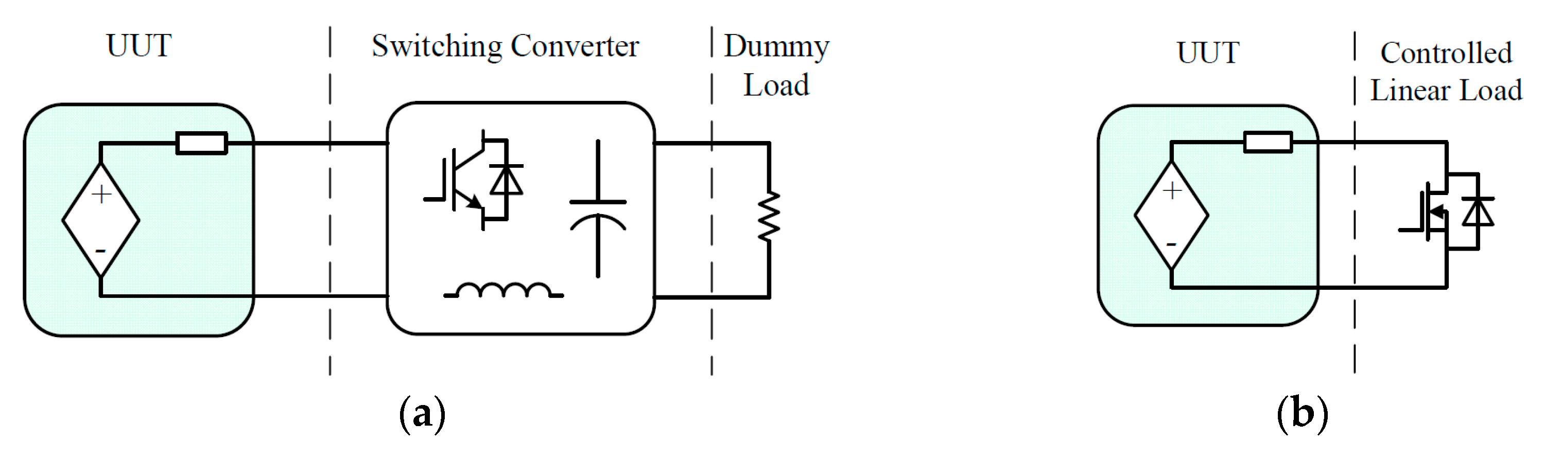
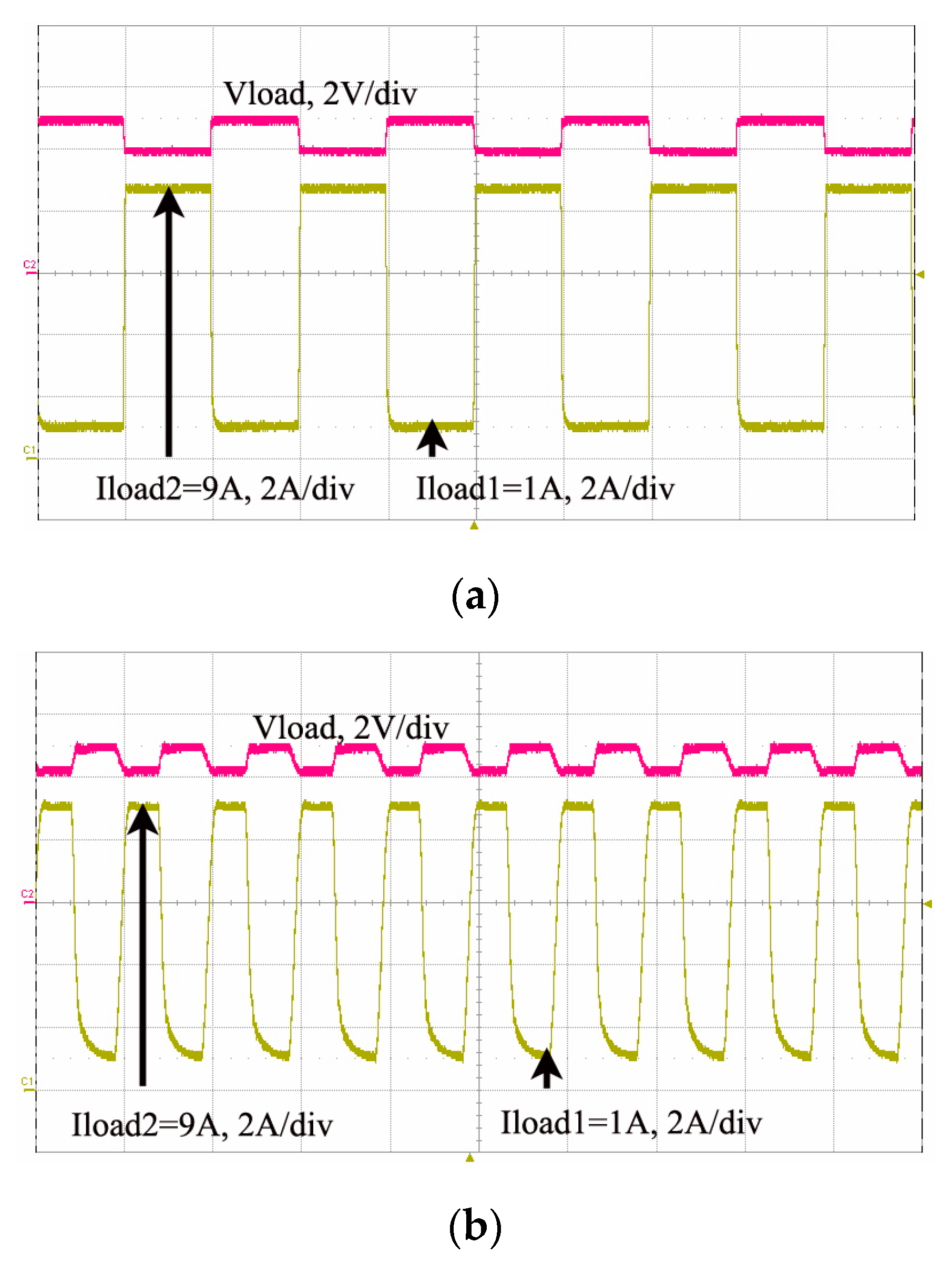
  • Constant current-sink. This method can test the static performance of the power supply systems, such as power level and dc output impedance.
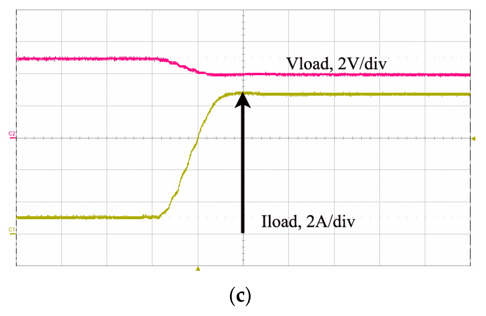
  • Pulsed/step current-sink. This test mode, UUT output voltage response is tested under step load current; the dynamic performance of the power supply systems can be evaluated by examining the voltage response.
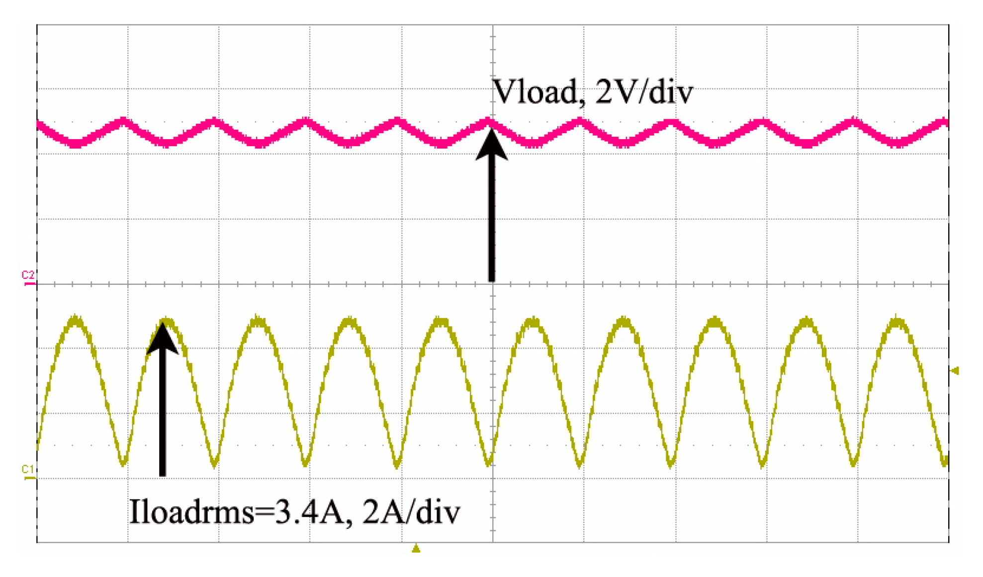
  • Programmed current-sink. Programmed current sink can test the performance of the power supply under nonlinear load excitation. This test mode is of increasing demand as the grid-tie inverters become more prevalent and introduce disturbances back into the dc systems.
The conventional approach to electronic load control is realized by the analog circuits. The analog-based control can guarantee precise regulation and tracking of certain load profiles, which are generated by signal synthetization blocks. The digital controller, which is capable of providing flexible and advanced control solution, is gaining a lot of attentions nowadays. The fully loaded control and communication peripherals of the DSC can yield very low component-count. However, in electronic load application, digital control is challenging; in order to drive the MOSFET device into the active region, gate charge has to be controlled based on the sampled current feedback. In order to accomplish the same task as the analog controller, the digital values generated from the digital controller can be converted to the analog values using digital-to-analog converter (DAC), which introduce excessive cost as well as the sampling-and-hold effect. This effect is undesirable as it will introduce current/voltage ripples and act similarly to a switching e-load.
In this paper, a linear electronic load using low-cost digital Pulse Width Modulation (PWM) peripherals is proposed. Wide Safe Operation Area (SOA) MOSFETs are regulated into the active region as the current sink. The interleaving PWM scheme is proposed for passive current ripple mitigation; through device selection, driver circuit design and layout design, 4-phase multiplexed current-sink is implemented with only one feedback current sensor. System identification method is proposed to obtain the power stage model by supplying Pseudo-Random Binary Sequence (PRBS) excitation under close-loop. The improved design is implemented later on with the identified model. The prototype is built and tested for a variety of current-sink modes for verification the effectiveness of the proposed design.

2. Digital Electronic Load System Design

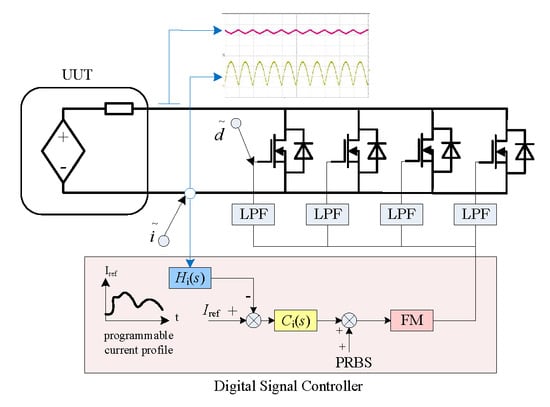
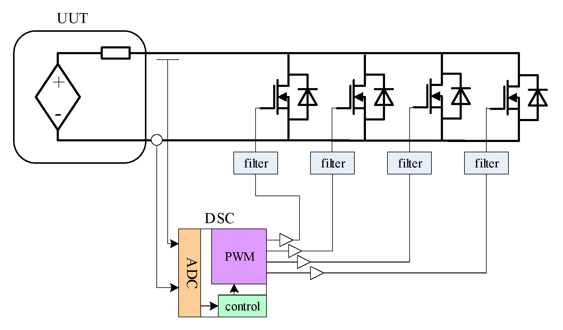
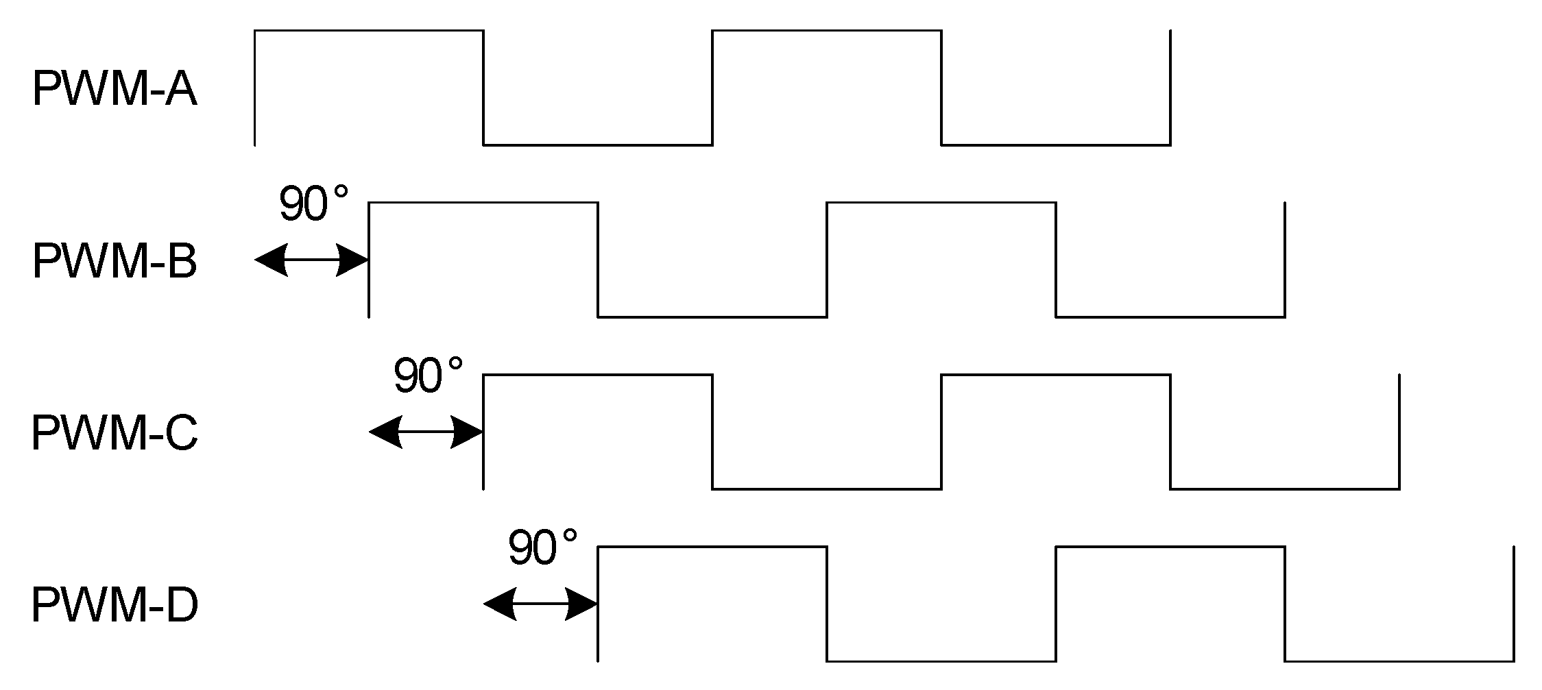
2.1. System Structure

As per discussed in Section 1, if the digital controller is used in the electronic load system, the DAC is required to convert the digital control values into analog form, which is not considered as optimal in terms of the conversion speed and the cost. Therefore, another option is explored in this research.
PWM module is the common peripheral in off-the-shelf DSCs. PWM signal filtered by a low-pass filter will remain its average value. Therefore, it is viable and economical to use PWM signals to generate the gate voltage. However, attenuation effect of the filter is no way to be perfect, the gate voltage ripple will propagate to the load current and cause load current ripple. As can be found from the datasheet of a FET device, the input characteristics of the active region is nonlinear and concave in shape, which means that a small deviation from the desired gate voltage will incur a large swing of drain current. If the filtered PWM signal is used, a method of ripple mitigation has to be proposed in order to reduce the drain current ripple.
The diagram of the proposed digital electronic load is shown in Figure 2. The power stage of the e-load consists of 4 power MOSFET in parallel, which is individually driven by the filtered PWM signal. In order to mitigate the current ripple induced by the remained ac components in the filtered PWM signal, each PWM signal is 90° phase-shifted to each other. The four channels of drain current are multiplexed in time domain, resulting in smaller current ripple. For load current regulation, single current loop is designed without active power sharing among the MOSFET devices. The total drain current is measured, conditioned and converted to the digital form; the digital control routine compares the real time current value with the current reference profile, amplifies the error signal, and loads the PWM with new duty cycle values. A gate driver circuit is connected in order to amplify the gate signals to a compatible level for MOSFET gate driver; a low-pass filter is used to eliminate the PWM ripples and generate a dc voltage to drive the MOSFETs.

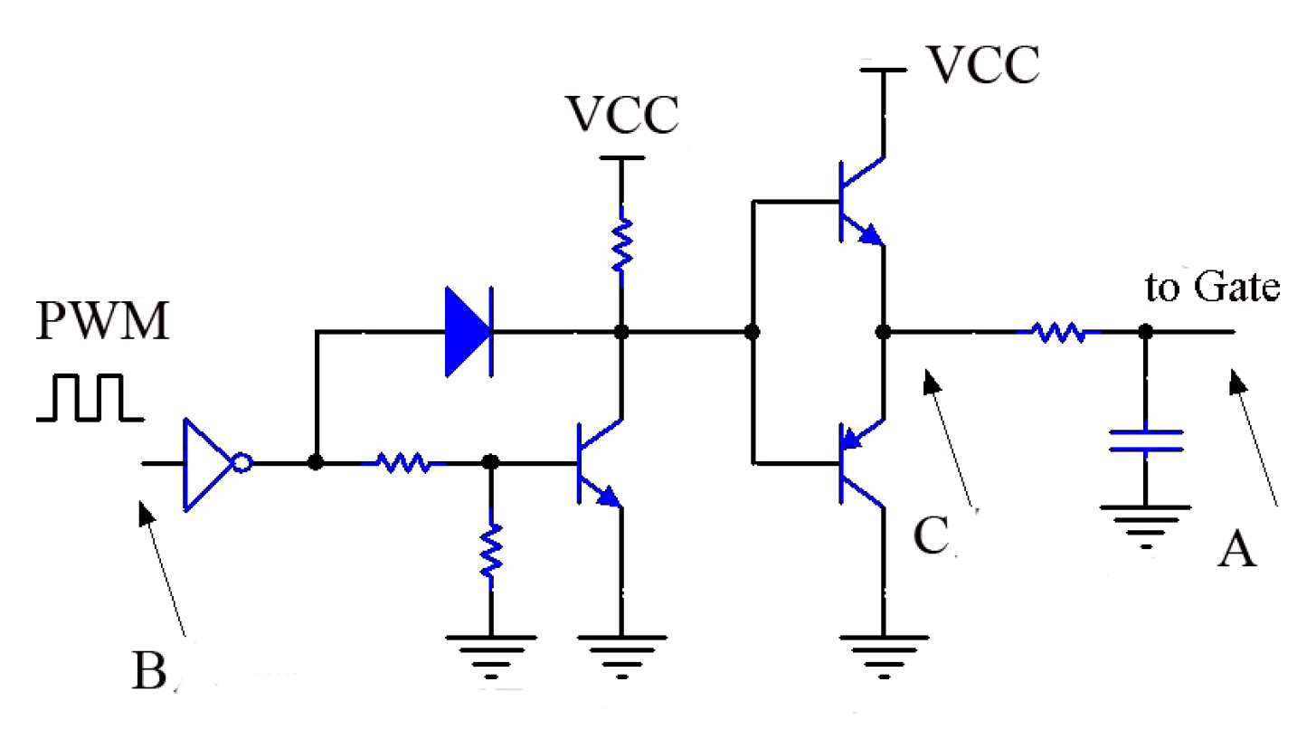
2.2. Power Devices and Drivers

Semiconductor device can be used as the power sink due to its fast response to control input. Field effect transistor device can be driven into active region by applying proper gate voltages; while bipolar transistor devices can be driven into linear region with proper base current injection. In the proposed design, the wide Safe Operation Area (SOA) MOSFET IXTH80N20L from IXYS is used as the power sink device. The breakdown voltage of the device is 200 V and I25 °C is 80 A. The drain-source voltage and drain current will be controlled such that the operation point of the load locates in the SOA.
The power MOSFET has a positive temperature coefficient (PTC), therefore, it is feasible to parallel multiple MOSFETs for high load current. Although switching at high frequency, there is no periodical charge and discharge of MOSFET gate capacitor for full capacity, the current rating of the gate driver circuitry can be selected to a low value. The gate driver is implemented with discrete components as indicated in Figure 3. To attenuate gate voltage ripple, a single-stage low pass filter (LPF) with 32 kHz cut-off frequency is applied to filter PWM voltage ac components.
The dsPIC33FJ DSC is chosen for control system implementation, which includes six pairs of complementary high-resolution PWM and 16 channels of 10-bit ADC. The PWM signals are synchronized in 90° phase-shift as indicated in Figure 4. 200 kHz is selected as the switching frequency in order to achieve better dynamic performance. Figure 5 shows the PWM signal propagation within the gate drive circuit (GDC) referring to Figure 3, the GDC offers fast amplification of the DSC signal, which can meet the design criterion. Figure 6 shows the ac coupled MOSFET gate voltages, as can be clearly seen, the drive signals are multiplexed in time, which can contribute to drain current ripple attenuation.

2.3. Sensing and Conditioning

A wide bandwidth (80 kHz) open loop hall-effect sensor is used in the design. The output voltage and input current relation is given in Equation (1), where VB is the sensor bias voltage and kiv is the voltage to current ratio of the sensor.
V = V B + k i v · I
The output of the hall-effect sensor is conditioned by a first-order passive RC LPF for noise suppression. By applying small signal perturbation, the transfer function of the transducer network can be found as
H i ( s ) = k i v R C s + 1
where the LPF is designed using a 100 Ω resistor and 1nF ceramic capacitor, and kiv = 66 mV/A according to the sensor data-sheet.

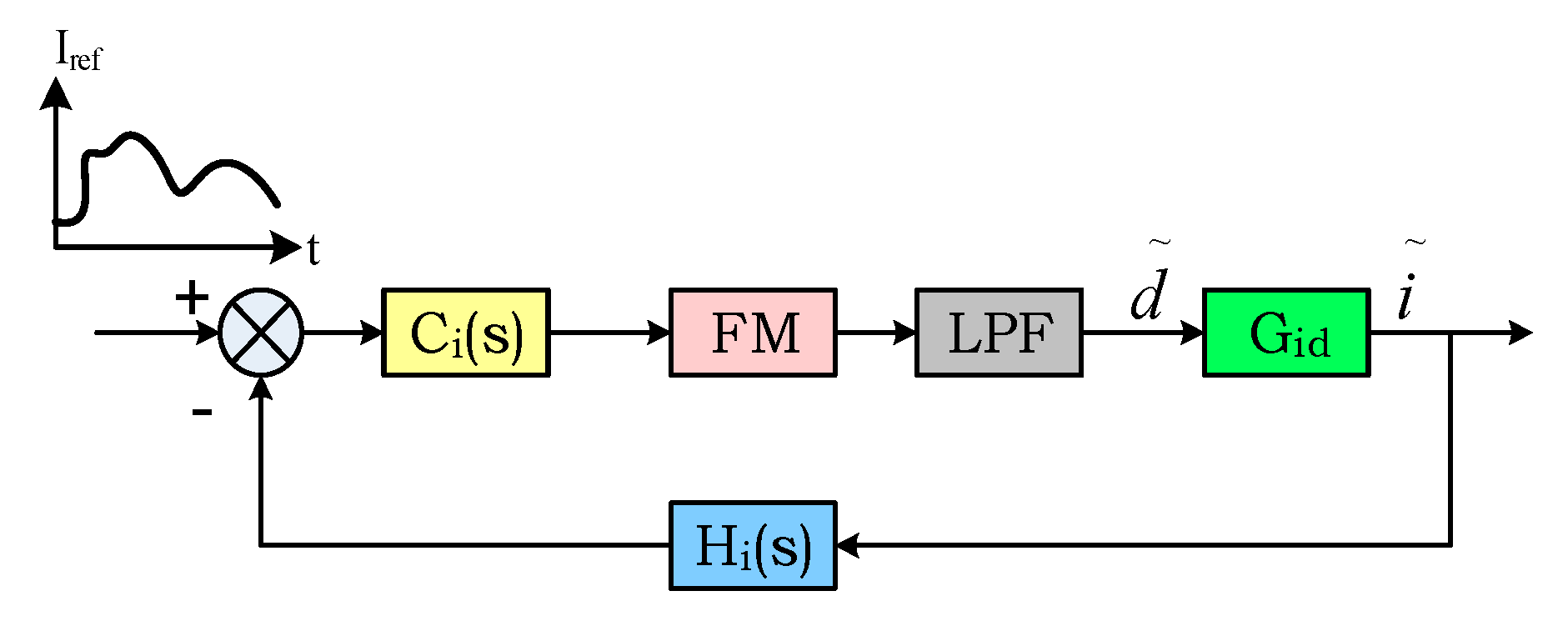
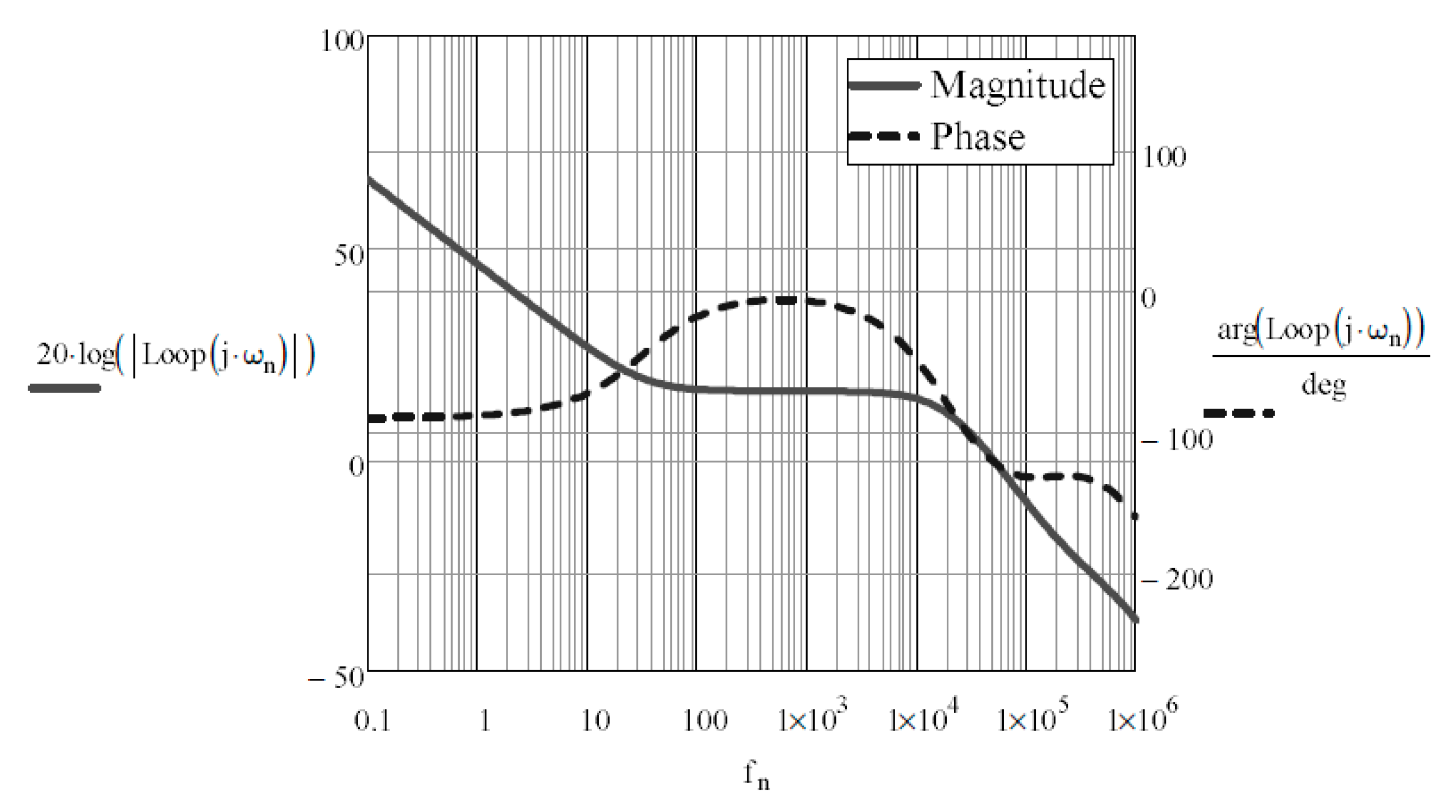
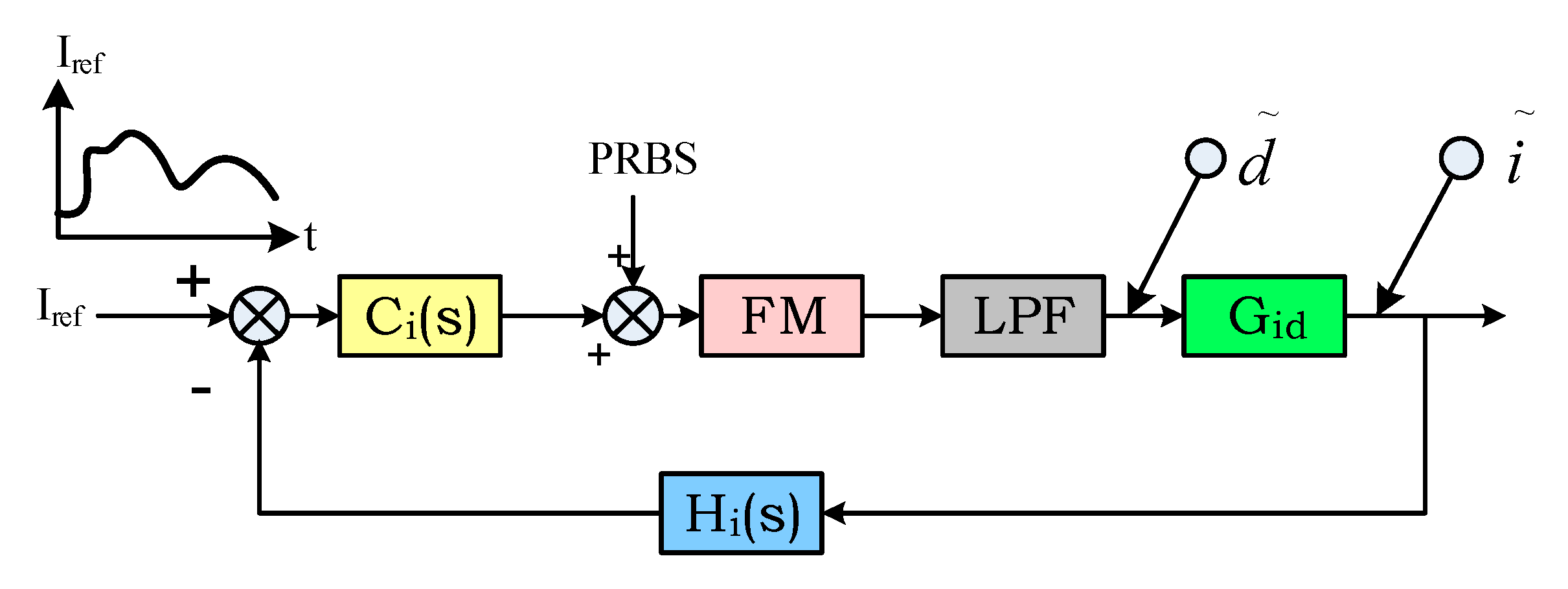
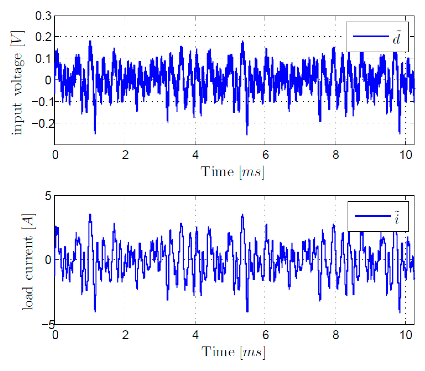
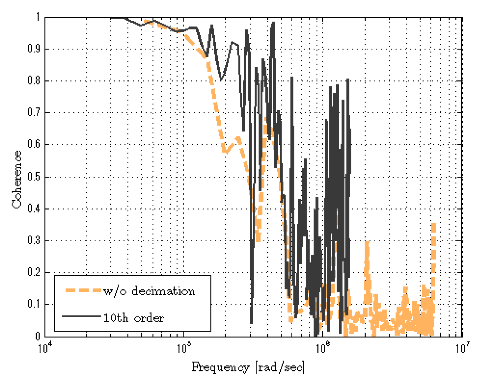
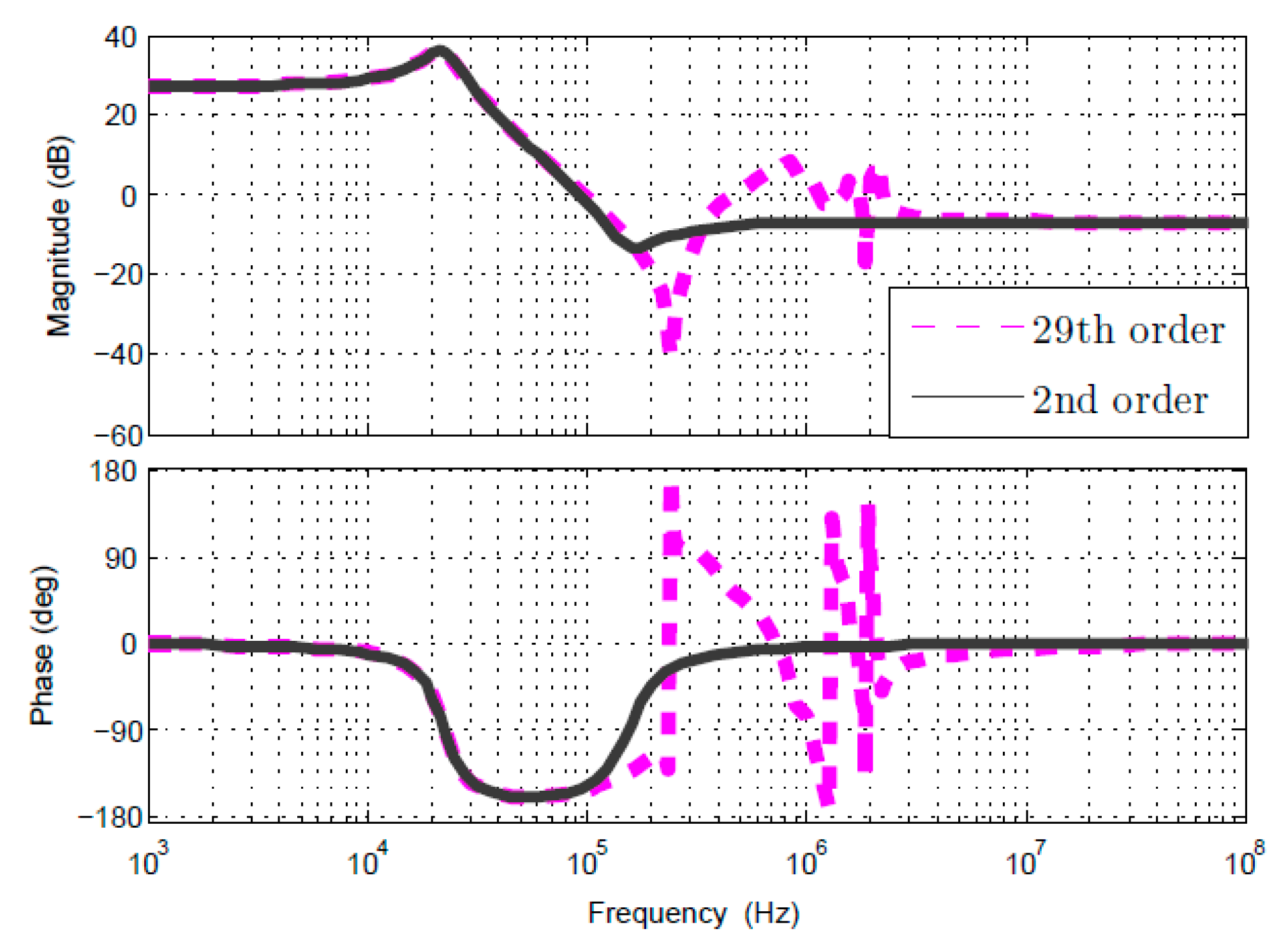
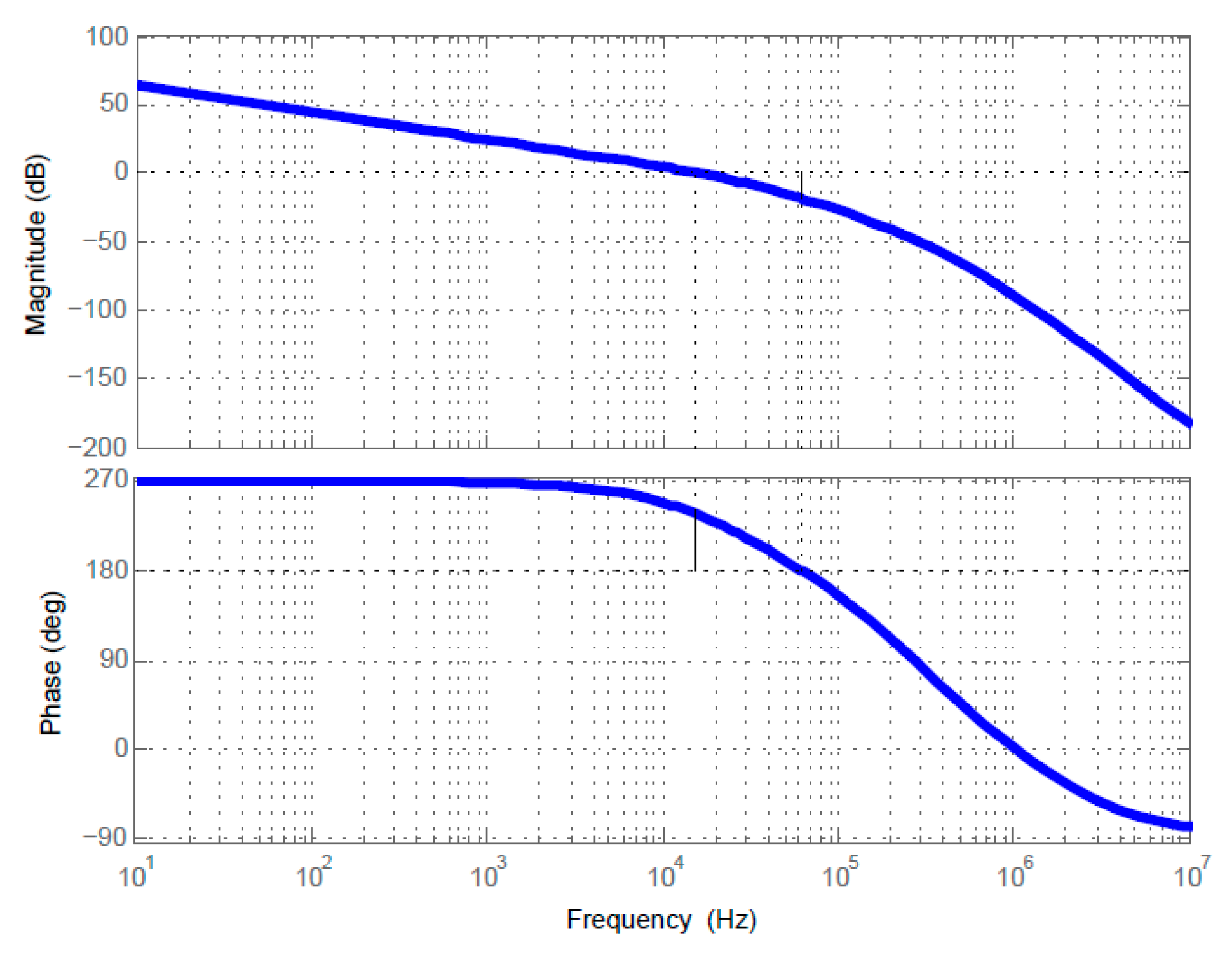
2.4. Model Identification and Control Loop Design

Although the device manufacturer has specified the static transfer characteristics of the MOSFET device, the drain current varies with device temperature, gate voltage as well as the load condition. Therefore, static mapping of the gate voltage and drain current is not possible for current sinking operation, the close loop control has to be implemented for the e-load to work under current-mode.
The control block diagram is shown in Figure 7. The Gid is the control-to-current transfer function of the power MOSFET, in this case, is the MOSFET input admittance. The Hi(s) is the small signal gain of the current transducer circuit. Ci(s) is the current controller. FM is the PWM modulation gain and LPF converts PWM signals into smoothed gate bias voltages.
An initial design of the current control loop in s-domain is carried out. Firstly, the small signal gain of the MOSFET Gid is obtained by differentiating the input admittance curve of the MOSFET numerically at 75 °C at 9 A. Then, a PID controller [15] is used for reference tracking with kp = 1, ki = 200, kd = 10−4, as shown in Figure 8, a cross-over frequency of 15 kHz and phase margin of 70° is achieved in the theoretical design process.
The bilinear transformation is applied to discretize the designed s-domain controller. The sampling frequency is set to 50 kHz and digital controller updates at each ADC interrupt routine.
Figure 9 shows the initial experimental results of a 4-phase e-load. As indicated in Figure 9a, under PID close-loop control, e-load can track the current command (step from 4 A to 8 A) in 400μs with attenuated current ripple. However, oscillation occurs after the reference change, which indicates weak system stability. The pulsed current sink experiment is also conducted, in which the e-load acts as the periodic current sink with ΔILoad = 4.48 A for transient test purposes. The test waveform in Figure 9b shows effective tracking of pulsed reference, the UUT voltage is showing expected variation under pulsed load. However, the waveform shows a similar manner of oscillation upon reference change, which is not desirable for the field test.
The parameters of the PID controller is adjusted in order to eliminate the oscillation; further test results indicate that system response becomes more sluggish as the steady state oscillation is attenuated. Therefore, a more precise plant model is required in order to improve the system performance.
Pseudo-Random Binary Sequence (PRBS) has wide power spectrum, which is suitable for the model identification [16]. In this research, the 9th order PRBS with 5% of full duty cycle is used as the excitation signal as indicated in Equation (3)
u [ n ] = U [ n ] + Δ u · s [ n ]
where U[n] is the output of the current controller at nth sampling time, Δu is the amplitude of the PRBS signal, s[n] is the binary bit generated by a 9th order PRBS generator with a period of 511.
The data probe is placed at the input and output of the plant respectively as shown in Figure 10, in which case are the gate voltage and drain current of MOSFET. The input and output data for system identification is plotted in Figure 11 with actual analog units. The coherence between the input and output signal is plotted in Figure 12. In order to improve the coherence under desired system cross-over frequency, a 10th order decimation filter is applied to the data. As indicated in the figure, decimated signal has improved coherence at the low frequency region below 100 kHz for linear controller design, which is sufficient for the targeted application.
Based on the ARX model, the system identification can be carried out by using the decimated input-output data. To decide the system model, the cross-validation method is introduced, in which case 29th order is selected. The bode plot of the 29th order model presents strong second order properties under the half of the switching frequency as shown in Figure 13. To facilitate the controller design, order reduction is performed using balanced realization method. The bode plot for the reduced order model is also presented in Figure 13, it can be observed that under 100 kHz, no significant variation exists between the high order and low order model. Therefore, the obtained 2nd order model can be used in the design. The transfer function of the plant can be found as in Equation (4)
G i d = k s 2 + 2 ξ n ω n s + ω n 2 s 2 + 2 ξ d ω d s + ω d 2
where the parameters are listed in Table 1. As the high frequency characteristics are of less interest in this design, further simplification is performed by eliminating the second order s-domain polynomials on the numerator, which results in a canonical second order system with a constant gain n 2 on the numerator.
In order to validate the identified model, the comparison between the experimental signal and the identified model with the PRBS excitation, which is not used for identification, is carried out. Figure 14 shows good agreement between simulation results with the identified model and the experimental data.
Zero-pole cancelation method is used in the current mode control system design; a 4th controller is proposed in Equation (5), where k is the static gain, the first 2nd order polynomial cancel the plant dynamics, the second 2nd order polynomial with double zero ωz1 cancel the poles of redesigned two stage LPF before the MOSFET gate, a pole at zero provide zero steady state error while the other three poles locating at 100 kHz provide switching ripple attenuation.
C ( s ) = k ( s 2 / ω d 2 + 2 ξ d s / ω d + 1 ) ( 1 + s / ω z 1 ) 2 s ( 1 + s / ω p ) 3
With the proposed controller, the compensated open-loop transfer function can be obtained. The bode plot of the transfer function is shown in Figure 15; the crossover frequency is 15.4 kHz with phase of 57°.

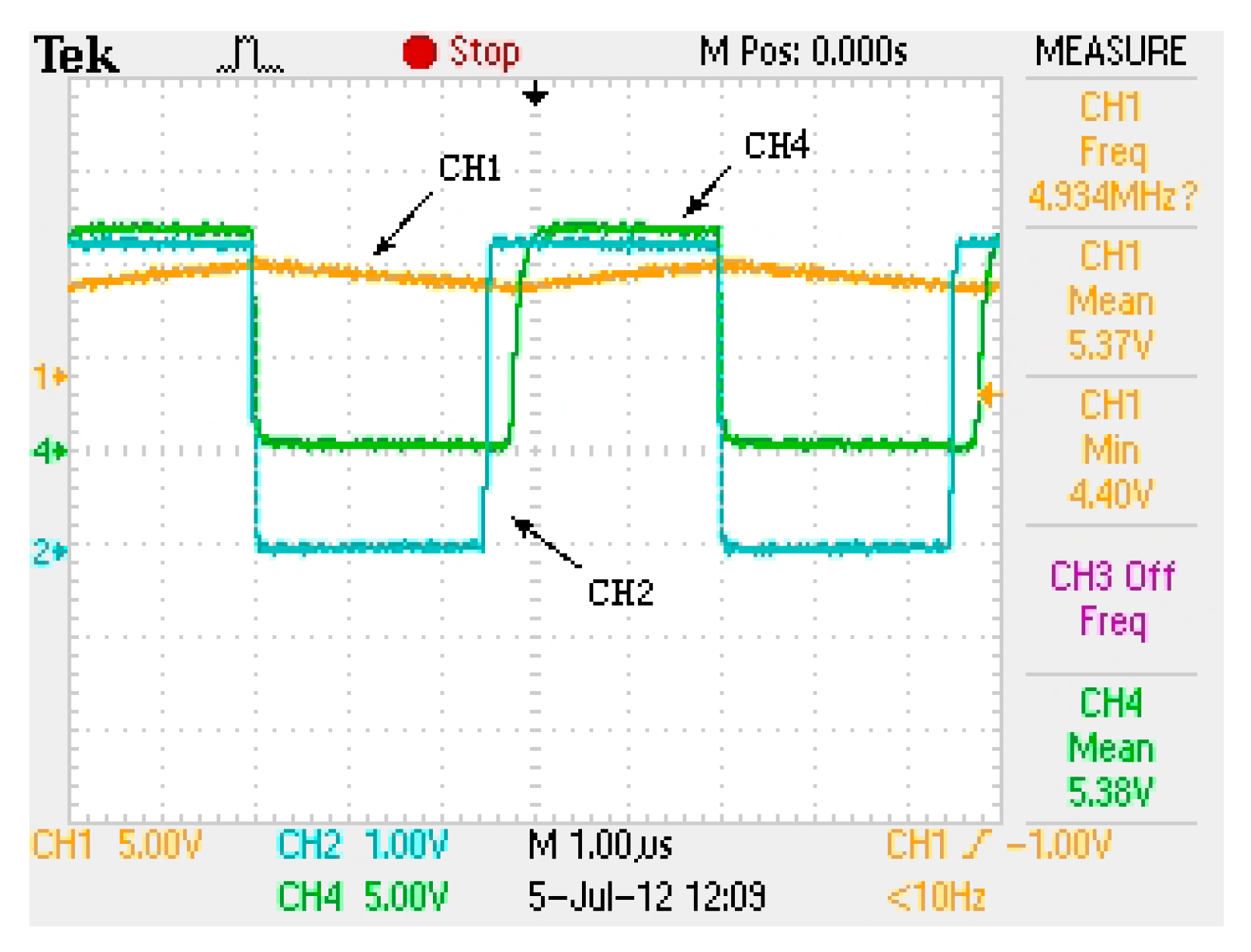
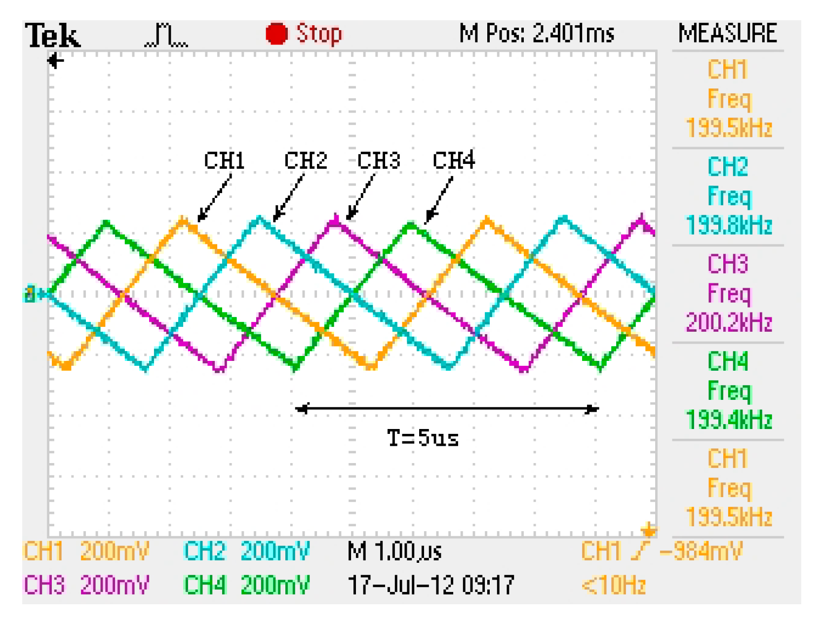
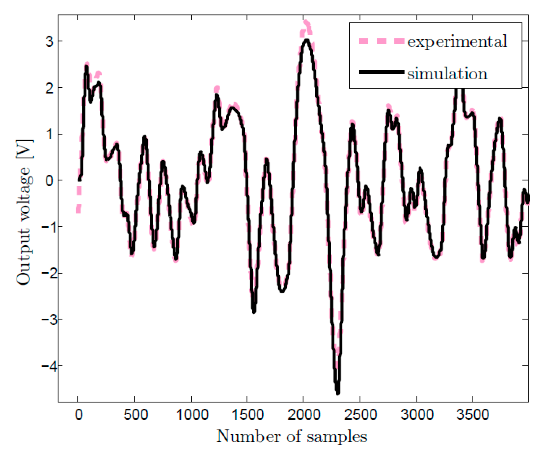
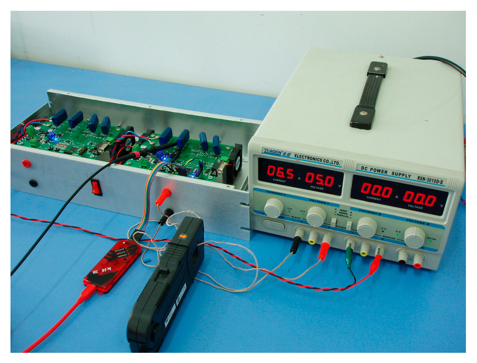
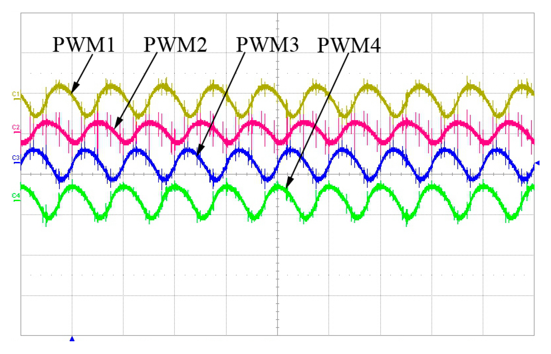
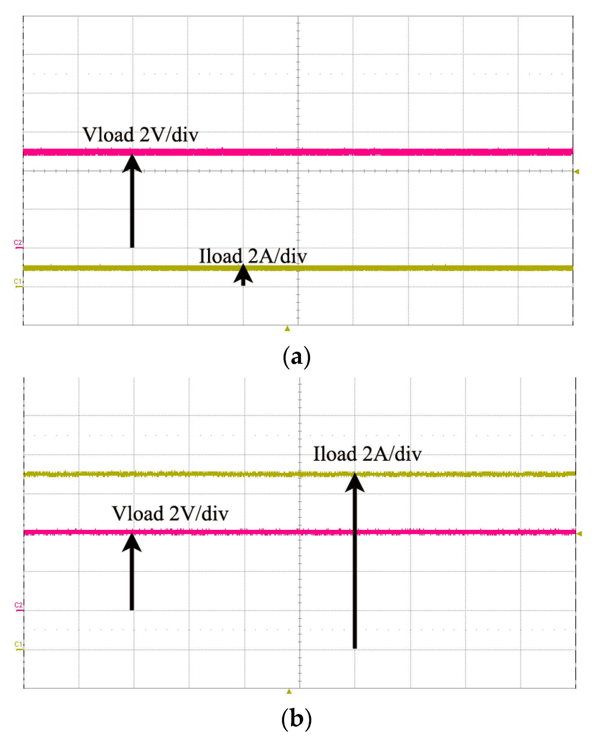
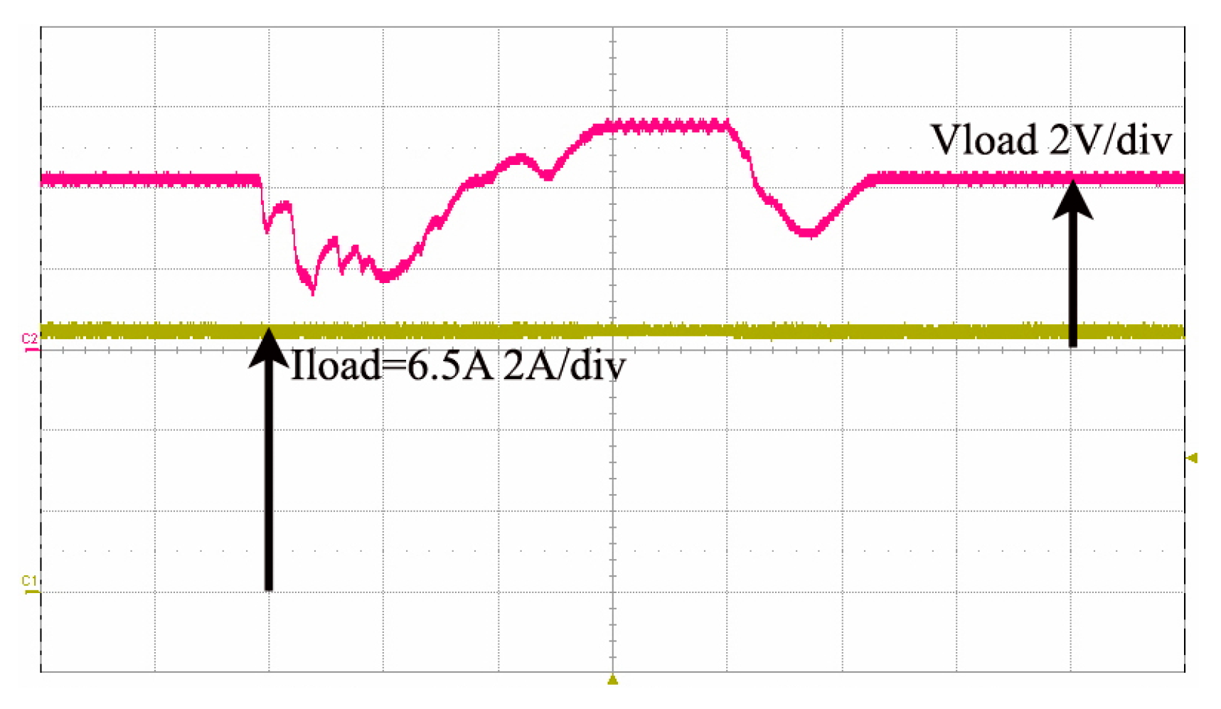
3. Experimental Results and Analysis

A 50 W 4-phase e-load prototype is built as shown in Figure 16, the micro-controller dsPIC33FJ64GS606 with high resolution PWM peripheral is used. In order to prevent the thermal runaway due to possible uneven power sharing, the MOSFET batch, the drivers’ parameters and the PCB layout have been carefully selected, designed and finally verified based on the power device case temperature differences. The UUT is a linear bench power supply with 30 V 10 A capability. The experimental verification is carried out for current (sink) mode, in which the UUT is supplying a variable dc voltage and the proposed e-load sinks current in a programmed manner. The test is conducted under a maximum sink current of 9 A under a variable UUT output voltage around 5 V.
Figure 17 shows the waveforms of the 4-phase PWM (AC coupled) signals filtered by an improved double-stage LPF; one can easily find that voltage ripple is reduced from 450 mVpp to 100 mVpp.
The steady state test waveforms for constant current sink mode are presented in Figure 18a for 10% load (1 A) and Figure 18b for 100% load (9 A); as shown in the figure, the load current ripple is well attenuated and load current ILoad can be controlled at the desired level, which indicates that the e-load can perform static test without introducing excessive load disturbances. The case temperature of the MOSFET is measured with infrared devices, which shows tolerable temperature difference with 1 °C.
Figure 19 shows the constant current sink mode (ILoad = 6.5 A) regulation when input source voltage (VLoad) is undergoing a large swing. It can be observed from the figure that the load current keeps constant with random input voltage variations.
Figure 20 shows the pulse current sink test results, where a pre-programmed pulse current profile is set up in the micro-controller. This mode of operation emulates the conditions of the intermittent load. As can be seen from Figure 20a, the load current ILoad is pulsating from 10% to full load with a frequency of 50 Hz. Comparing to the previous results, the oscillation during the steady state is eliminated due to more precise modeling of the plant. The output voltage of UUT (VLoad) is showing periodical voltage variation due to its output impedance, which indicates that the regulation speed of the UUT could not follow the load variation. 500 Hz pulse current load is also tested, the waveform is presented in Figure 20b. The rising edge of the pulse current is shown in Figure 20c. With the designed digital control loop, 123 μs of rise time is achieved, the load current overshoot is limited to 1%, which is sufficient for most of the linear power supply tests. A commercial bench-mark electronic load (BK8500) is also tested in the mean time for the same operation condition, the rise time is found to be 1.6 ms. The proposed digital e-load is found to have a much faster response.
Finally, the nonlinear load condition is emulated. The well-known 100 Hz ripple injection scenario from a single-phase grid-tie inverter load is emulated. Under the assumption that the UUT has a large output dc capacitor, a 100 Hz rectified sinusoidal current is drawn from the UUT. Figure 21 shows this testing scenario when the load current (ILoadRMS = 3.4 A) is of rectified sinusoidal shape. As expected, the UUT terminal voltage presents a disturbed dc voltage with 100 Hz ripple component.

4. Conclusions

In this paper, a linear electronic load using digital pulse width modulation is proposed. To solve the high current ripple problem in a digital PWM system, a multi-phase and double-stage LPF scheme is used. Low-cost single current loop without additional active power sharing is designed. System identification methods based on PRBS excitation is applied to obtain the power stage model, which is later verified by simulation results. The control system is designed using pole-zero cancelation technique and implemented in a digital signal controller. The experimental results on constant current sink mode, pulse current sink mode, and inverter current sink mode show satisfactory steady state performance and stable transient response. The proposed system can achieve commensurate performance with benchmark e-load under current sink mode, which indicates its potential for the fully digitalized power testing equipment in the near future.

Author Contributions

Conceptualization, W.J.; methodology, W.J. and S.H.; software, W.J. and S.H.; validation, W.J., J.W. and S.X.; formal analysis, W.J.; investigation, J.W.; resources, Q.W.; data curation, J.W.; writing—original draft preparation, W.J.; writing—review and editing, Q.W. and Z.L.; visualization, W.J.; supervision, W.J.; project administration, W.J.; funding acquisition, W.J. and Z.L.

Funding

This research was jointly supported by National Natural Science Foundation of China (Grant No. 31571765), Natural Science Foundation of Jiangsu Province, China (Grant No. BK20170503) and Yangzhou City-Yangzhou University joint Grant (No. SCX2017020021)

Acknowledgments

The conference version of this paper is published in the IEEE PEDS 2013, titled “Digitally controlled multi-phase electronic current sink” coauthored by W.J., S.W., S.K., L.X., S.H. However, in the fully extended journal version, we report on the methodology of designing a fast and low-cost electronic load using improved digital modulation, model identification, and control.

Conflicts of Interest

The authors declare no conflict of interest.

References

  1. Emadi, A. Modeling of power electronic loads in ac distribution systems using the generalized state-space averaging method. IEEE Trans. Ind. Electron. 2004, 51, 992–1000. [Google Scholar] [CrossRef]
  2. Ramirez, J.; Torres, E. An electronic load controller for the self-excited induction generator. IEEE Trans. Energy Convers. 2007, 22, 546–548. [Google Scholar] [CrossRef]
  3. Singh, B.; Rajagopal, V. Neural-network-based integrated electronic load controller for isolated asynchronous generators in small hydro generation. IEEE Trans. Ind. Electron. 2011, 58, 4264–4274. [Google Scholar] [CrossRef]
  4. Shamsi, P.; Fahimi, B. Dynamic behavior of multiport power electronic interface under source/load disturbances. IEEE Trans. Ind. Electron. 2013, 60, 4500–4511. [Google Scholar] [CrossRef]
  5. Rao, Y.S.; Chandorkar, M.C. Real-time electrical load emulator using optimal feedback control technique. IEEE Trans. Ind. Electron. 2010, 57, 1217–1225. [Google Scholar]
  6. Grubic, S.; Amlang, B.; Schumacher, W.; Wenzel, A. A high-performance electronic hardware-in-the-loop drive cload simulation using a linear inverter (linverter). IEEE Trans. Ind. Electron. 2010, 57, 1208–1216. [Google Scholar] [CrossRef]
  7. Jiang, W.; Wang, S.; Kan, S.; Xie, L.; Hashimoto, S. Digitally controlled multi-phase electronic current sink. In Proceedings of the 2013 IEEE 10th International Conference on Power Electronics and Drive Systems (PEDS), Kitakyushu, Japan, 22–25 April 2013; pp. 862–866. [Google Scholar]
  8. Kazerani, M. A high-performance controllable dc load. In Proceedings of the IEEE International Symposium on Industrial Electronics, Vigo, Spain, 4–7 June 2007; pp. 1015–1020. [Google Scholar]
  9. Zhang, R.; Zhang, Z.; Chen, J. Analysis and design of repetitive controlled power electronic load simulator with high dynamic performance. In Proceedings of the IEEE 6th International Power Electronics and Motion Control Conference, Wuhan, China, 17–20 May 2009; pp. 2603–2607. [Google Scholar]
  10. Rosas-Caro, J.; Peng, F.Z.; Cha, H.; Rogers, C. Z-source-converter-based energy-recycling zero-voltage electronic loads. IEEE Trans. Ind. Electron. 2009, 56, 4894–4902. [Google Scholar] [CrossRef]
  11. Borrell, A.; Castilla, M.; Miret, J.; Matas, J.; de Vicuna, L.G. Control design for multiphase synchronous buck converters based on exact constant resistive output impedance. IEEE Trans. Ind. Electron. 2013, 60, 4920–4929. [Google Scholar] [CrossRef]
  12. Sattar, A.; Tsukanov, V. Mosfets withstand stress of linearmode operation. Power Electron. Technol. 2007, 34–39. [Google Scholar]
  13. Mishra, S.; Ngo, K.D.T. Dynamic characterization of the synthetic ripple modulator in a tightly regulated distributed power application. IEEE Trans. Ind. Electron. 2009, 56, 1164–1173. [Google Scholar] [CrossRef]
  14. Upadhyay, S.; Mishra, S.; Joshi, A. A wide bandwidth electronic load. IEEE Trans. Ind. Electron. 2012, 59, 733–739. [Google Scholar] [CrossRef]
  15. Franklin, G.F.; Powell, J.D.; Emami-Naeini, A. Feedback Control of Dynamic Systems, 5th ed.; Pearson Education: London, UK, 2006. [Google Scholar]
  16. Ljung, L. System Identification-Theory for the User, 2nd ed.; Prentice Hall: Upper Saddle River, NJ, USA, 1999. [Google Scholar]
Figure 1. Electronic load types (a) switching e-load (b) linear e-load.
Energies 12 02611 g001
Figure 2. System structure.
Energies 12 02611 g002
Figure 3. MOSFET gate drive.
Energies 12 02611 g003
Figure 4. Four-phase interleaving PWM signals.
Energies 12 02611 g004
Figure 5. Gate signal propagation (CH1- test point A voltage, CH2- test point B voltage, CH4- test point C voltage).
Energies 12 02611 g005
Figure 6. Four-phase signal (AC coupled).
Energies 12 02611 g006
Figure 7. Current control loop.
Energies 12 02611 g007
Figure 8. Frequency response of PID compensated open-loop transfer function.
Energies 12 02611 g008
Figure 9. Test results with PID controller (a) step response from 4 A to 8 A, (b) 60 Hz pulse current sink mode (10 ms/div).
Energies 12 02611 g009
Figure 10. Plant identification using PRBS under close-loop conditions.
Energies 12 02611 g010
Figure 11. Plant input and output signals for identification (AC coupled).
Energies 12 02611 g011
Figure 12. Coherence plot between system input and output signal.
Energies 12 02611 g012
Figure 13. Identified model bode plots.
Energies 12 02611 g013
Figure 14. Simulation results and experimental data comparison.
Energies 12 02611 g014
Figure 15. Simulation results and experimental data comparison.
Energies 12 02611 g015
Figure 16. Low-power electronic load test bed.
Energies 12 02611 g016
Figure 17. 4 MOSFET gate voltages (AC coupled 100 mV, 1 μs/div).
Energies 12 02611 g017
Figure 18. Constant current sink test (a) 10% load current (1 ms/div), (b) 100% load current (1 ms/div).
Energies 12 02611 g018
Figure 19. Constant current sink with input voltage variation (2 s/div).
Energies 12 02611 g019
Figure 20. Pulse current sink mode (a) 50 Hz pulse current test (10 ms/div), (b) 500 Hz pulse current test (2 ms/div), (c) step response (200 μs/div).
Energies 12 02611 g020aEnergies 12 02611 g020b
Figure 21. 100 Hz inverter load current emulation test (10 ms/div).
Energies 12 02611 g021
Table 1. Parameters of the plant model.
Kξnξdωnωd
0.560.40.221.1 × 1061.8 × 105

