Article

Switching Device Dead Time Optimization of Resonant Double-Sided LCC Wireless Charging System for Electric Vehicles

1
School of Mechanical Engineering, Shanghai Jiao Tong University, Shanghai 200240, China
2
National Engineering Laboratory for Electric Vehicles, School of Mechanical Engineering, Beijing Institute of Technology, Beijing 100081, China
*
Authors to whom correspondence should be addressed.
Energies 2017, 10(11), 1772; https://doi.org/10.3390/en10111772
Submission received: 19 September 2017 / Revised: 30 October 2017 / Accepted: 30 October 2017 / Published: 3 November 2017
(This article belongs to the Special Issue The International Symposium on Electric Vehicles (ISEV2017))

Abstract

:
Aiming at the reduction of the influence of the dead time setting on power level and efficiency of the inverter of double-sided LCC resonant wireless power transfer (WPT) system, a dead time soft switching optimization method for metal–oxide–semiconductor field-effect transistor (MOSFET) is proposed. At first, the mathematic description of double-sided LCC resonant wireless charging system is established, and the operating mode is analyzed as well, deducing the quantitative characteristic that the secondary side compensation capacitor C2 can be adjusted to ensure that the circuit is inductive. A dead time optimization design method is proposed, contributing to achieving zero-voltage switching (ZVS) of the inverter, which is closely related to the performance of the WPT system. In the end, a prototype is built. The experimental results verify that dead time calculated by this optimized method can ensure the soft switching of the inverter MOSFET and promote the power and efficiency of the WPT.

1. Introduction

Electric vehicles (EVs) have gained popularity in recent years, for their inherent environmental benefits of reduced gas emissions [1,2]. Battery systems and charging techniques are the most critical technology supporting EV market penetration [3]. As a new wireless power transfer technology, the resonant wireless power transfer (WPT) technology, which is based on magnetic field coupling between the transmitting and receiving coils, has been seen development in recent years [4]. Compared with the traditional charging method (e.g., plug-in), the WPT technology eases drivers from the problem of cable-exposure, tripping hazards, and risks on the snowy or rainy days [5]. In addition, with the characteristics of flexible application, safety, and reliability, WPT technology has been applied to various applications, such as medical implantation equipment, underwater robots, and electric vehicle (EV) charging [6,7].
A typical EV WPT system consists of AC/DC (PFC and BUCK circuit), DC/AC (inverter circuit), resonant compensation network, transmitting coil and receiving coil, rectifier, and battery [8]. The inverter circuit is used to transfer DC power into high frequency square wave voltage, which is key for the compensation network to achieve resonance. This paper adopts a full-bridge inverter circuit to meet high power EV charging conditions. In the inverter, if the upper and lower leg of the MOSFET are switched on at the same time, it will lead to short circuit, once the input voltage is too high, the MOSFET will be damaged. Therefore, it is required that a pair of the MOSFETs be switched on until another pair of MOSFETs are completely switched off, which means there should be dead-time between the drive signals.
Therefore, to improve the efficiency of the WPT system, it is necessary to adopt an optimal dead-time. Most previous work on the dead-time focused on the buck or boost circuit [9], all of which are required to sample the load current or voltage, increasing the complexity of control. Other work [10] has analyzed the relation between the optimal dead-time and turn-off related switching parameter, but it did not focus on the resonant compensation network. In [8], the double-sided LCC resonant compensation network and its tuning method was proposed, which realizes unity power factor at both the input and output. Moreover, tuning the secondary series capacitor C2 provides the zero-voltage switching (ZVS) condition for the MOSFET of the inverter, however, the paper did not propose a specific dead-time design method. Therefore, in this paper, a dead-time design method is proposed, by tuning the secondary series capacitor C2 to ensure the circuit is inductive. Considering the parasitic capacitor of the MOSFET, it is crucial to adopt the optimal dead-time to improve the power and efficiency of the WPT system. An inappropriate dead-time will lead to damage of MOSFETs.
In this paper, the dead-time optimization method of ZVS is studied in the double-sided LCC resonant compensation network. The mathematical equivalent model of the double-sided LCC resonant compensation network is established, and the relation between the equivalent impedance phase of the primary side and the incremental capacitance of the secondary side capacitor C2 is obtained in Section 2. Section 3 analyzes the process of charge and discharge of the parasitic capacitor of the MOSFET in a switching period, then the influence of the dead-time on the soft-switching is discussed. In the case of fixed secondary series compensation capacitor C2, the optimization method of the dead-time is proposed in Section 4. Experimental results verify the feasibility and correctness of the proposed method in Section 5. Finally, Section 6 concludes this paper.

2. Analysis of Double-Sided LCC Resonant Compensation Network Equivalent Characteristic

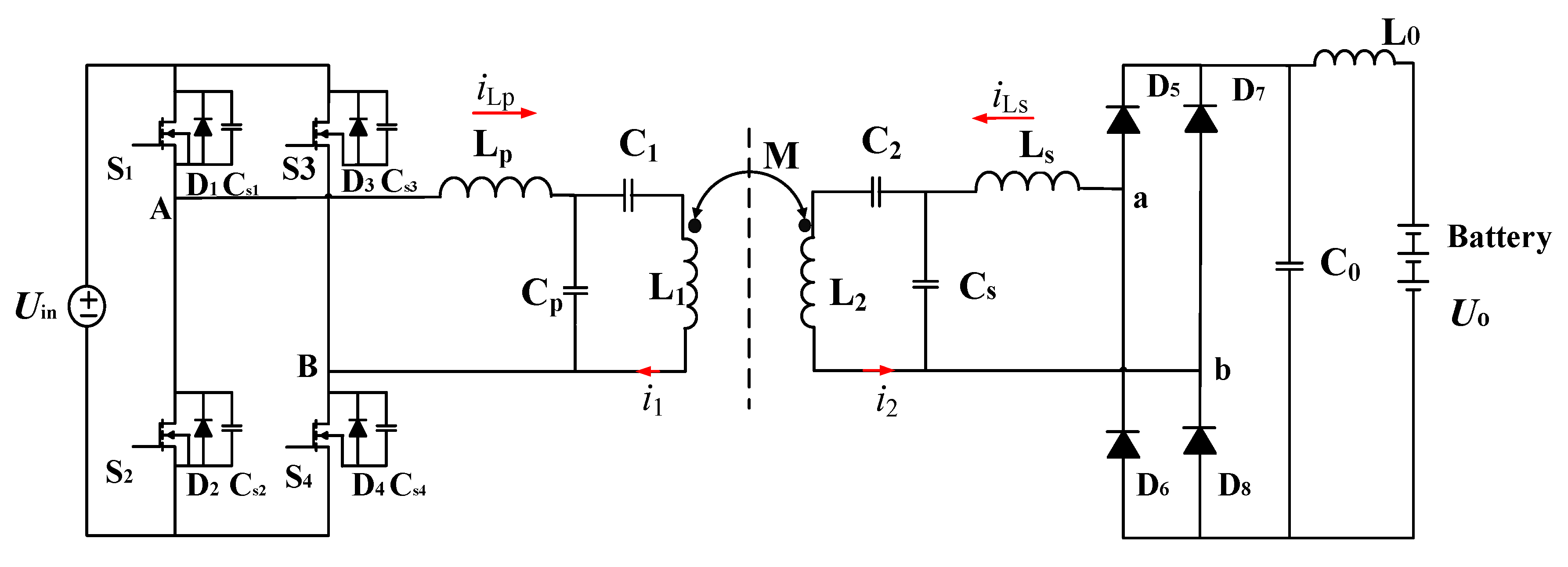
The configuration of the double-sided LCC resonant WPT system is shown in Figure 1. The inverter consists of four MOSFETs (S1~S4) and parasitic capacitors (Cs1~Cs4), parasitic antiparallel diodes (D1~D4). L1 and L2 are the self-inductances of the transmitting and receiving coils, respectively. Lp, Cp, and C1 are the primary side compensation inductor and capacitors. Ls, Cs, and C2 are the secondary side compensation components, the secondary side is symmetrical to the primary side. M is the coefficient inductance of the two main coils. The rectifier consists of fast recovery diodes (D5~D8), a filtering capacitor Co, and a filtering inductor Lo.
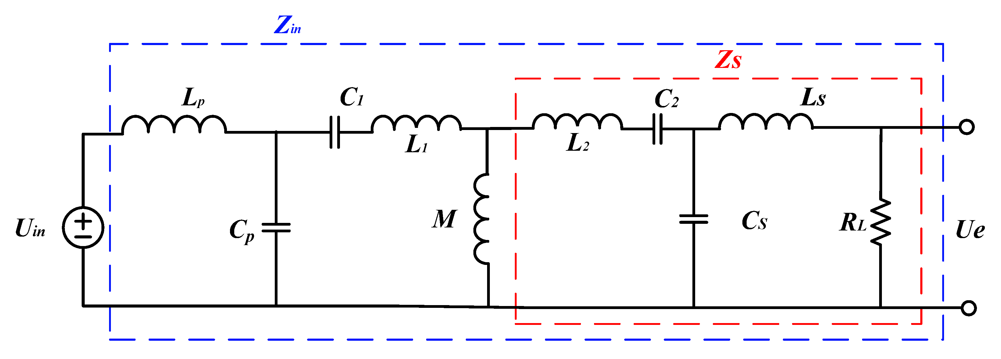
For the convenience of analysis, the parasitic resistance of the capacitors, inductors, and coils are ignored. The primary and secondary resonant compensation equivalent network is shown in Figure 2 [11]. Where U e = 2 2 π U o . Where RL represents the equivalent impedance of the battery and rectifier. According to [8], the receiving terminal can realize the unity power factor, thus, the equivalent impedance can be represented as a pure resistance, defined as R L = π 2 U o 2 8 P o u t , Pout is the output power of the WPT system.
The equivalent impedance of the secondary side circuit is
Z s = ( R L + j ω 0 L s ) 1 j ω 0 C s R L + j ω 0 L s + 1 j ω 0 C s + j ω 0 L 2 + 1 j ω 0 C 2
where ω 0 is the resonant frequency.
The equivalent impedance of secondary side Zr was reflected to the primary side by the mutual inductance M of the coils, Zr is defined as
Z r = ω 0 2 M 2 Z s
Therefore, the equivalent impedance of the primary side is defined as
Z i n = ( j ω 0 L 1 + 1 j ω 0 C 1 + Z r ) 1 j ω 0 C p j ω 0 L 1 + 1 j ω 0 C 1 + Z r + 1 j ω 0 C p + j ω 0 L p
According to [5], the parameters of double-sided LCC resonant compensation network are designed by the following equations
{   L p C p = 1 ω 0 2    ,     L s C s = 1 ω 0 2    , L 1 L p = 1 ω 0 2 C 1   ,   L 2 L s = 1 ω 0 2 C 2  
Substitute (2) and (4) into (1) and (3), the equivalent impedance of the equivalent double-sided LCC compensation network is given by
Z i n = ω 0 2 L p 2 L s 2 M 2 R L
It is a pure resistant load. In this case, the inverter output voltage is in phase with the output current, and unity power factor achieves, but it is not a suitable condition for MOSFETs to achieve ZVS. According to [8], by tuning the secondary series capacitor C2, making the circuit be inductive and thus providing conditions for the MOSFET to achieve ZVS.
After tuning the C2, the equivalent impedance of the primary side circuit is
Z i n = R + j X
here ΔC2 is the incremental value, R = ω 0 2 L p 2 L S 2 M 2 R L , X = L p 2 ω 0 M 2 Δ C 2 ( C 2 + Δ C 2 ) C 2 .
As is known, the ZVS condition mainly depends on the variation of load resistance and mutual inductance, in this paper, by using the equivalent resistance Zin, which relates to the load resistance RL and mutual inductance M, as (5) and (6) shown above. It is a simple method to integrate various conditions into one variable.

3. Time Domain Analysis of the Double-Sided LCC Compensation Network

3.1. Time Domain Analysis of Switching Mode

To facilitate the analysis, the following assumptions are made [12]:
  • All the MOSFETs and diodes are ideal;
  • All the capacitors, inductors and coils are ideal;
  • Cs1 = Cs2 = Cs3 = Cs4 = Coss, where Coss is the output capacitor of the MOSFET;
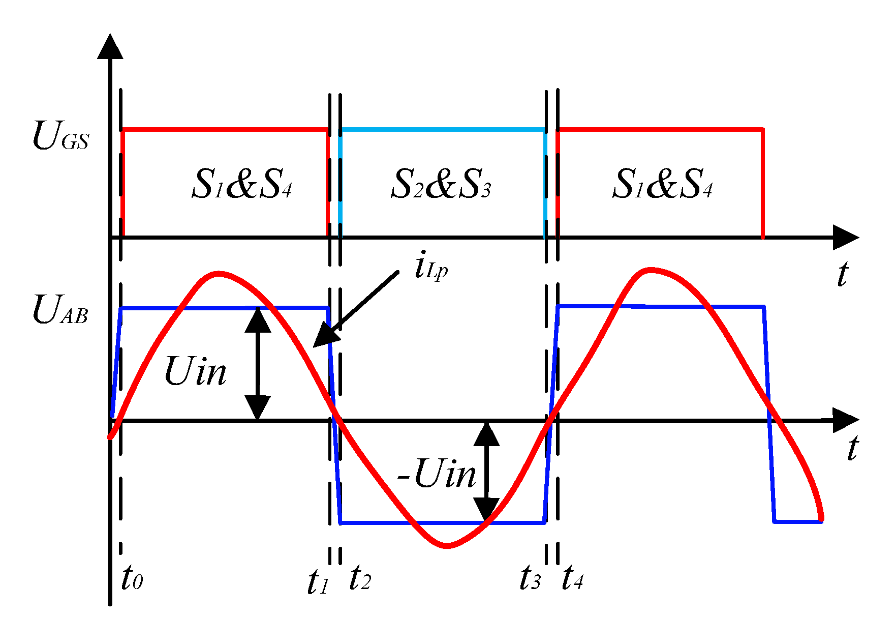
Considering the dead-time, the main operating waveform is shown in Figure 3.
A switching cycle can be divided into four stages. The first half switching cycle is analyzed.
Mode 1 (t0, t1): before the S1 and S4 are turned on, the inverter output current iLp is freewheeling through D1 and D4, Cs1 and Cs4 has been discharged to zero voltage. At the moment t1, S1, and S4 achieve zero voltage turn-on. UAB = Uin at this time.
Mode 2 (t1, t2): at t1, both the S1 and S4 are turned off, the inverter output current iLp (the instantaneous current when MOSFET turned off is called cut-off current) is charging the capacitor Cs1 and Cs4 to voltage Uin, while capacitors Cs2 and Cs3 are discharged to zero voltage.
The mode 3 and mode 4 are similar to mode 1 and mode 2, respectively. By tuning the capacitor C2 and dead-time optimization, the turn-off current can be minimized and reduce the MOSFET turn-off loss.

3.2. The Influence of Dead-Time on Soft-Switching

From the above analysis, the inverter output current charges and discharges the parasitic capacitors of the MOSFET during the dead-time. If the dead-time is set inappropriately, it will lead to a lower transmitting power and efficiency. Therefore, the dead-time setting is crucial for MOSFET to achieve ZVS.
Take the left arm of the inverter as an example, if the dead-time is set too short, the S1 will be turned on before the parasitic capacitor completely discharged, at the moment S1 is turned on, the parasitic capacitor short-circuits and produces an impulse current on the MOSFET, if the impulse current is larger than the pulsed drain current of the MOSFET, the MOSFET will break down.
If the dead-time is set too long, when the parasitic capacitor C1 has been discharged completely, while the S1 do not be turned on, C1 is involved in the circuit resonant, and to be charged again, making S1 fail to achieve ZVS. It is found that there is a positive current on the S1 before the S1 is switched on, which will also produce an impulse current on the S1.

4. Optimization Method of Dead-Time of Inverter MOSFET

According to the above analysis, to ensure MOSFETs achieve ZVS and reduce the switching loss, on the one hand, the dead-time should be large enough to charge or discharge both the MOSFET’s and PCB’s parasitic capacitor, on the other hand, it is required that the inverter current be close to zero at the switching point, which means the dead-time should smaller than the diode freewheeling time. Therefore, the dead-time is required to meet with the expression
t c + t o f f < t D T < t d
where tc is the time of charging and discharging the parasitic capacitors, toff is the turn-off time of MOSFET, and td is the diode freewheeling time.

4.1. Calculation of Parasitic Capacitor Charging Time

Since the time for charging and discharging the parasitic capacitor is relatively short compared to a switching period, the turn-off current Ioff can be approximately regarded as constant. According to [13], the time of parasitic capacitor charging and discharging is defined as
t c = ( 2 C o s s + C s t r a y ) U i n I o f f
where Cstray is the parasitic capacitor of PCB.
Considering the high order harmonics of the square voltage [14], the inverter first order output current is defined as
I L p _ 1 s t = 2 U i n | Z i n | sin ( ω t + θ 1 s t )
where θ1st is the phase angle of the first order input impedance. At the moment MOSFET is turned off, t = π, the first order turn-off current is
I o f f _ 1 s t = 2 U i n X R 2 + X 2
Similarly, the high order turn-off current is given by
I o f f _ ( 2 k + 1 ) t h 2 U i n _ ( 2 k + 1 ) t h X ( 2 k + 1 ) t h R ( 2 k + 1 ) t h 2 + X ( 2 k + 1 ) t h 2
Therefore, the total turn-off current can be given by
I o f f = I o f f _ 1 s t + k = 1 I o f f _ ( 2 k + 1 ) t h = 2 U i n X R 2 + X 2 + k = 1 2 U i n 2 k + 1 X ( 2 k + 1 ) t h R ( 2 k + 1 ) t h 2 + X ( 2 k + 1 ) t h 2

4.2. Calculation of Diode Freewheeling Time

From the above analysis, at the end of the diode freewheeling, another pair MOSFETs should be turned on, which means when the equivalent inductor of the circuit was completely discharged, the inverter current should be zero [15]. In fact, by using MATLAB, according to (7), all the high order current lags behind the inverter output voltage UAB by about 90°. Figure 4 shows the effect of the high order harmonic current on the inverter current.
From Figure 4, it is found that the zero-crossing point of the inverter current is mainly decided by the third harmonic current. Thus, the dead-time roughly meets with the following expression
I L p _ 3 r d = 2 I r m s _ 3 r d sin ( 3 ω 0 t d + θ 3 r d )
So the diode freewheeling time is given by
t d = θ 3 r d 360 1 3 f
where f is the inverter switching frequency and θ3rd is the phase angle of the third order input impedance.

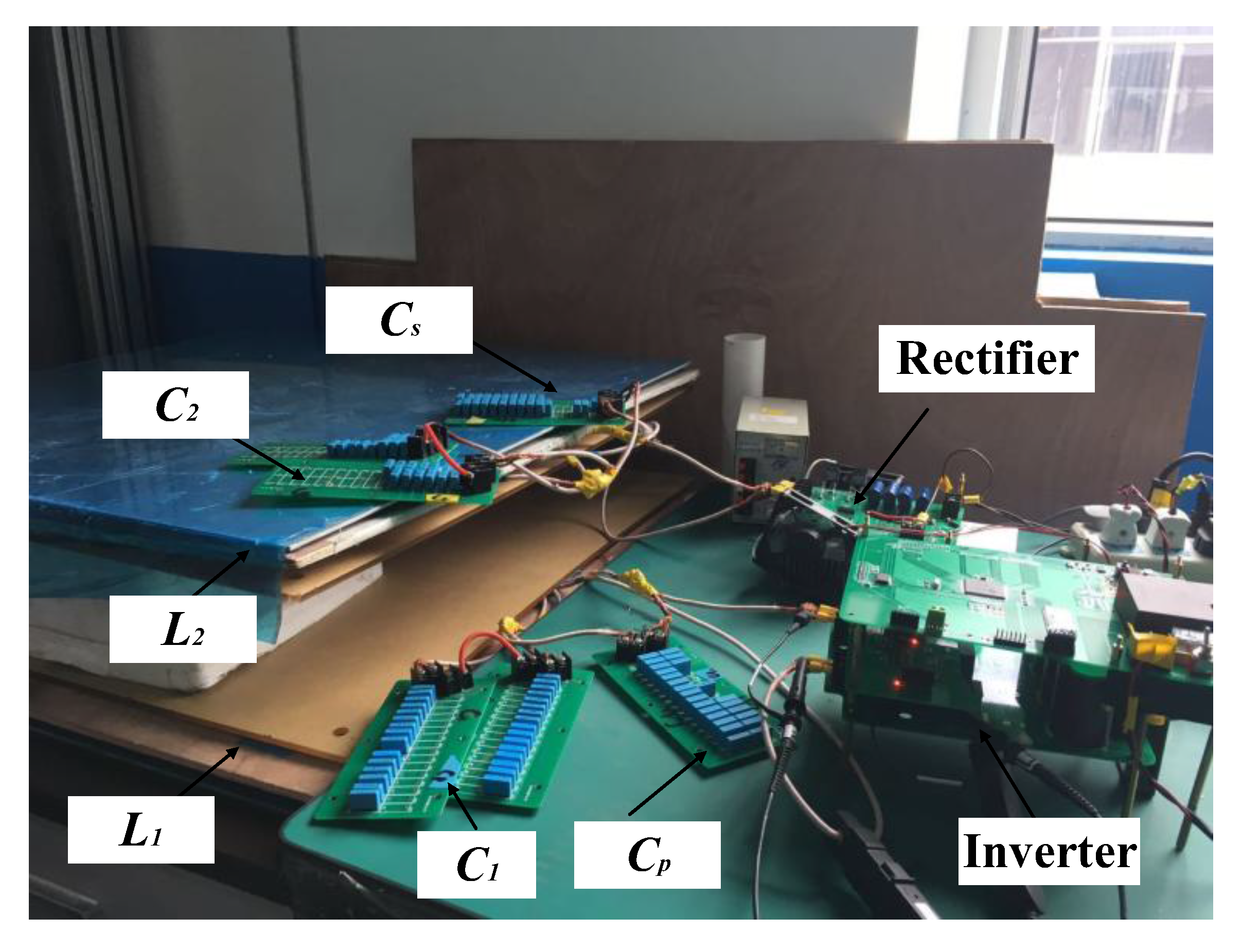
5. Experiment Results

In order to validate the optimization method of dead time of switching devices in double-sided LCC resonant WPT system, a prototype is established, the experimental platform is shown in Figure 5.
The input voltage Uin = 100 V, output voltage Uo = 48 V, resonant frequency f = 95 kHz, the transfer gap h = 150 mm. The parameter of the double-sided LCC resonant WPT system are listed in Table 1.
By increasing the capacity of C2, the WPT system circuit is inductive, the specific capacity of C2 can be set according to practical application, for convenience, in this paper we set ΔC2 = 1 nF.
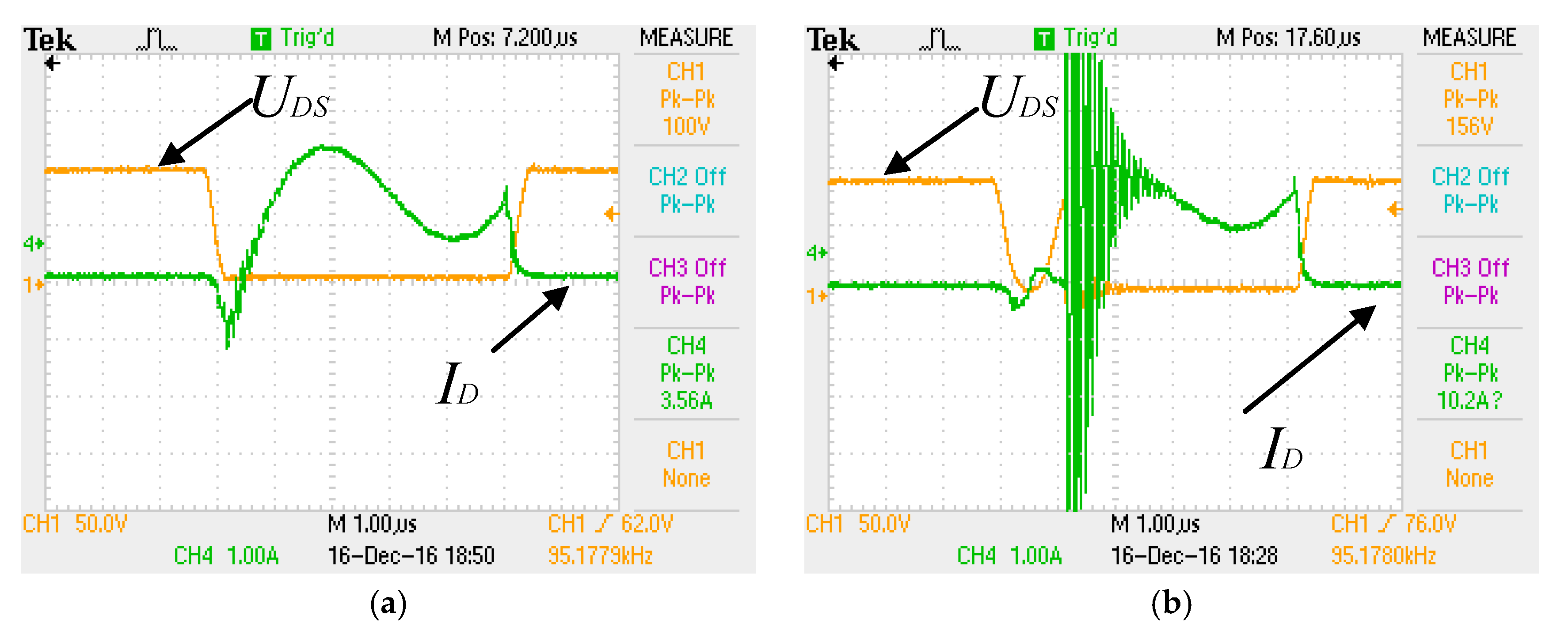
In this work, Infineon IPW60R070C6 CoolMOS MOSFET is chosen as the inverter switches, its turn-off time is 88 ns, output capacitor Coss = 215 pF. From the above analysis and parameters, it can be calculated that the dead-time should meet with the expression:
325   ns < t D T < 875   ns
Considering the increase of MOSFET temperature, which may lead to the increase of MOSFET turn-on and turn-off time, the optimal dead-time is set 500 ns.
Figure 6 shows the voltage and current of MOSFET when tDT = 500 ns, tDT = 1.2 us, respectively.
From Figure 6a, before MOSFET turned on, there is negative current on the MOSFET because of the diode freewheeling, when the drive voltage UGS go rise to 90%, the MOSFET has forward current (ID) and the MOSFET achieve zero voltage switch on. From Figure 6b, because of the long dead-time, before the MOSFET is turned on, there is positive current on the MOSFET, even after the MOSFET is turned off, the voltage of the switch drops sharply to zero.
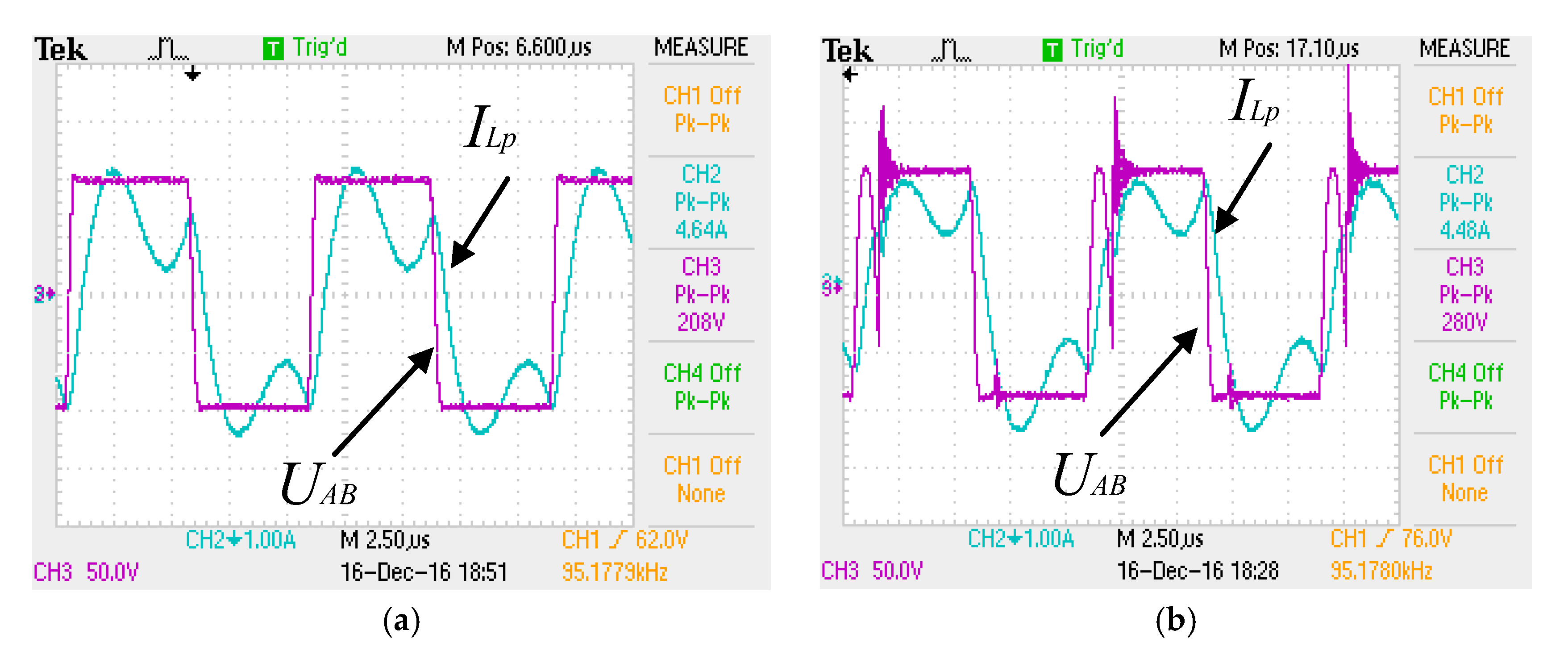
Figure 7 shows the voltage and current of inverter when tDT = 500 ns, tDT = 1.2 us, respectively.
From Figure 7b, if the dead-time is too large, there is high frequency oscillation of the inverter. From the experimental results, a dead-time setting that is too short or too long will lead to distortion output voltage and current of the inverter, causing a lower efficiency and transmitting power of the WPT system.
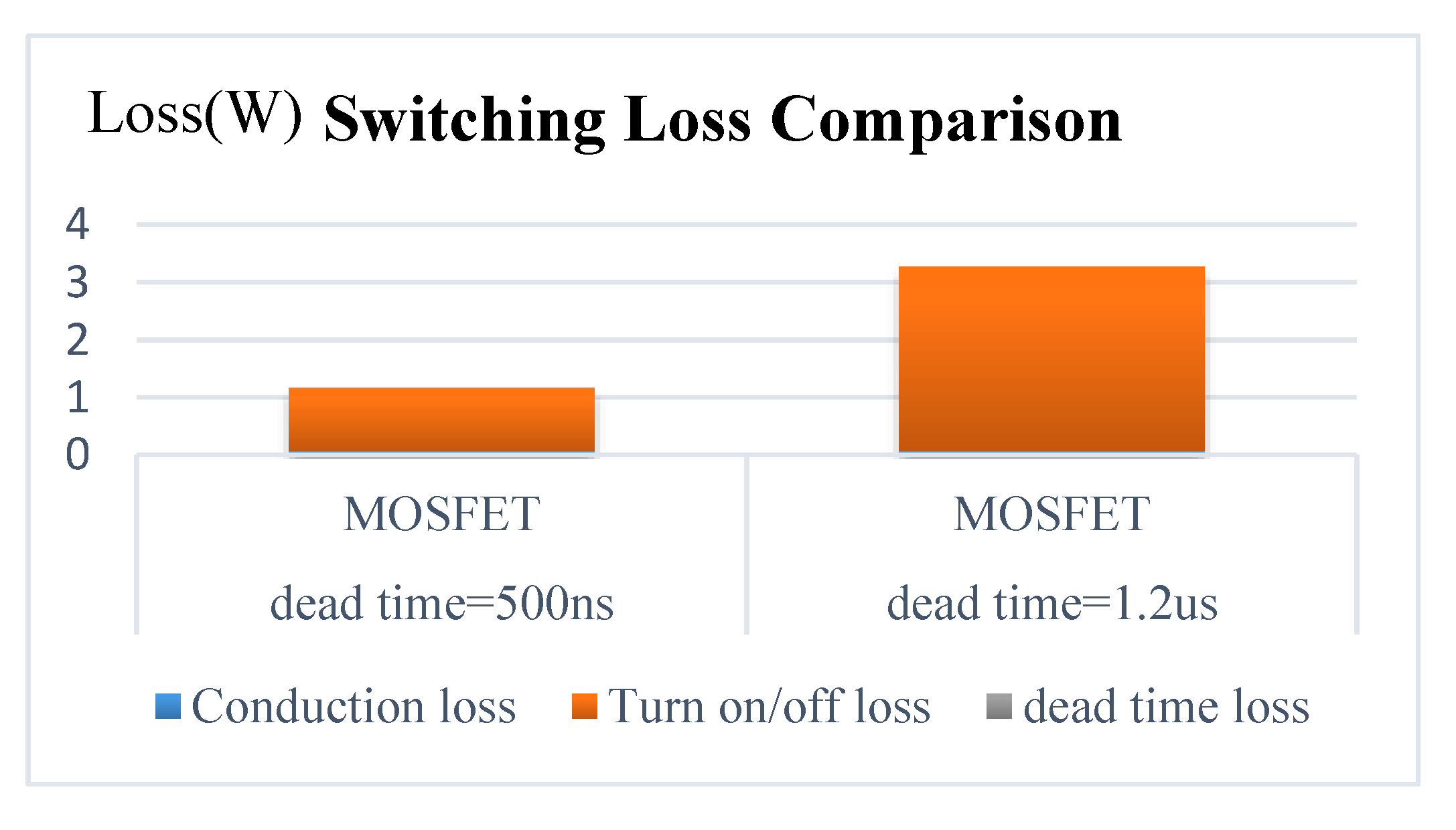
It is known that the longer the dead time, the less effective value of the inverter voltage. When the input power is about 100 W, in Figure 8, the conduction loss of both the dead-time situations is about 0.02 W, much less than the switching loss. It also shows that the turning on/off loss is much smaller if the proper dead time is chosen. By selecting the optimal dead time, the MOSFETs can achieve ZVS and eliminate voltage and current distortion, promoting transmitting efficiency.

6. Conclusions

In this paper, the problem of soft-switching of the MOSFET in the double-sided LCC resonant WPT system is studied and analyzed. Based on the theoretical calculation of the equivalent impedance, the condition of MOSFET to achieve ZVS is verified. By analyzing the time-domain model of a switching period, the influence of dead-time on MOSFET is studied. Finally, an optimization of switching device dead-time of double-sided LCC WPT system is proposed. The feasibility of this method is verified by experiment results.

Acknowledgments

This work was supported in part by the National Natural Science Foundation of China under Grant No. 51677118, the Joint Funds of the National Natural Science Foundation of China under Grant No. U1564206, the Science and Technology Commission of Shanghai Municipality under Grant 16510711500 and 16PJD030, Beijing Municipal Science and Technology Project under Grant No. Z171100000917013, the National Science and Technology Support Program under Grant No. 2015BAG04B00, and International Science & Technology Cooperation Program of China under contract No. 2016YFE0102200.

Author Contributions

Xi Zhang proposed the original idea and built the mathematical model. Ziyang Lai developed all the hardware. Rui Xiong helped improve the parameter analysis. Zhe Li did some simulation work. Zhiming Zhang designed the primary and secondary coils. Liang Song completed the software. All authors carried out the data analysis, discussed the results and contributed to writing the paper.

Conflicts of Interest

The authors declare no conflict of interest.

References

  1. Chen, C.; Xiong, R.; Shen, W. A lithium-ion battery-in-the-loop approach to test and validate multi-scale dual H infinity filters for state of charge and capacity estimation. IET Power Electron. 2018, 33, 332–342. [Google Scholar] [CrossRef]
  2. Xiong, R.; Yu, Q.; Wang, L.; Lin, C. A novel method to obtain the open circuit voltage for the state of charge of lithium ion batteries in electric vehicles by using H infinity filter. Appl. Energy 2017, 207, 341–348. [Google Scholar] [CrossRef]
  3. Xiong, R.; Zhang, Y.; He, H.; Zhou, X.; Pecht, M. A Double-Scale, Particle-Filtering, Energy State Prediction Algorithm for Lithium-Ion Batteries. Available online: https://doi.org/10.1109/TIE.2017.2733475 (accessed on 1 November 2017).
  4. Li, S.; Mi, C.C. Wireless Power Transfer for Electric Vehicle Applications. IEEE J. Emerg. Sel. Top. Power Electron. 2015, 3, 4–17. [Google Scholar]
  5. Madawala, U.K.; Neath, M.; Thrimawithana, D.J. A Power–Frequency Controller for Bidirectional Inductive Power Transfer Systems. IEEE Trans. Ind. Electron. 2013, 60, 310–317. [Google Scholar] [CrossRef]
  6. Ning, P.; Miller, J.M.; Onar, O.C.; White, C.P. A compact wireless charging system for electric vehicles. In Proceedings of the 2013 IEEE Energy Conversion Congress and Exposition, Denver, CO, USA, 15–19 September 2013; pp. 3629–3634. [Google Scholar]
  7. Wu, H.H.; Gilchrist, A.; Sealy, K.D.; Bronson, D. A High Efficiency 5 kW Inductive Charger for EVs Using Dual Side Control. IEEE Trans. Ind. Inform. 2012, 8, 585–595. [Google Scholar] [CrossRef]
  8. Li, S.; Li, W.; Deng, J.; Nguyen, T.D.; Mi, C.C. A Double-Sided LCC Compensation Network and Its Tuning Method for Wireless Power Transfer. IEEE Trans. Veh. Technol. 2015, 64, 2261–2273. [Google Scholar] [CrossRef]
  9. Lee, S.; Jung, S.; Huh, J.; Park, C.; Rim, C.T.; Cho, G.H. Robust and efficient synchronous buck converter with near-optimal dead-time control. In Proceedings of the 2011 IEEE International Solid-State Circuits Conference, San Francisco, CA, USA, 20–24 February 2011; pp. 392–394. [Google Scholar]
  10. Zhang, Z.; Wang, F.; Costinett, D.J.; Tolbert, L.M.; Blalock, B.J.; Lu, H. Dead-time optimization of SiC devices for voltage source converter. In Proceedings of the 2015 IEEE Applied Power Electronics Conference and Exposition (APEC), Charlotte, NC, USA, 15–19 March 2015; pp. 1145–1152. [Google Scholar]
  11. Liu, C.; Ge, S.; Guo, Y.; Li, H.; Cai, G. Double-LCL resonant compensation network for electric vehicles wireless power transfer: Experimental study and analysis. IET Power Electron. 2016, 9, 2262–2270. [Google Scholar] [CrossRef]
  12. Hou, J.; Chen, Q.; Wong, S.C.; Tse, C.K.; Ruan, X. Analysis and Control of Series/Series-Parallel Compensated Resonant Converter for Contactless Power Transfer. IEEE J. Emerg. Sel. Top. Power Electron. 2015, 3, 124–136. [Google Scholar]
  13. Kundu, U.; Yenduri, K.; Sensarma, P. Accurate ZVS Analysis for Magnetic Design and Efficiency Improvement of Full-Bridge LLC Resonant Converter. IEEE Trans. Power Electron. 2017, 32, 1703–1706. [Google Scholar] [CrossRef]
  14. Zeng, H.; Yang, S.; Peng, F.Z. Design Consideration and Comparison of Wireless Power Transfer via Harmonic Current for PHEV and EV Wireless Charging. IEEE Trans. Power Electron. 2017, 32, 5943–5952. [Google Scholar] [CrossRef]
  15. López, V.M.; Navarro-Crespin, A.; Schnell, R.; Brañas, C.; Azcondo, F.J.; Zane, R. Current Phase Surveillance in Resonant Converters for Electric Discharge Applications to Assure Operation in Zero-Voltage-Switching Mode. IEEE Trans. Power Electron. 2012, 27, 2925–2935. [Google Scholar] [CrossRef]
Figure 1. Schematic of double-sided LCC resonant compensation network.
Energies 10 01772 g001
Figure 2. Equivalent schematic of double-sided LCC resonant compensation network.
Energies 10 01772 g002
Figure 3. Operation waveform of the inverter.
Energies 10 01772 g003
Figure 4. Effect of high order inverter current.
Energies 10 01772 g004
Figure 5. Experiment platform.
Energies 10 01772 g005
Figure 6. Voltage and current of MOSFET (a) tDT = 500 ns; (b) tDT = 1.2 us.
Energies 10 01772 g006
Figure 7. Voltage and current of inverter (a) tDT = 500 ns; (b) tDT = 1.2 us.
Energies 10 01772 g007
Figure 8. Switching loss comparison.
Energies 10 01772 g008
Table 1. Double-sided LCC resonant WPT system parameter.
ParameterValue
Transmitting (receiving) coil L1(L2)/uH260
Compensation inductor Lp, Ls/uH66
Mutual inductor M/uH67.6
Parallel capacitor Cp, Cs/nF42.3
Primary series capacitor C1/nF14.4
Secondary series capacitor C2/nF15.4
Output equivalent resistance RL25.8

